
IRFHM8228PbF
HEXFET
®
Power MOSFET
Base part number
Package Type
Standard Pack
Form
Quantity
IRFHM8228PbF
PQFN 3.3 mm x 3.3 mm
Tape and Reel
4000
IRFHM8228TRPbF
Orderable Part Number
V
DSS
25
V
R
DS(on)
max
(@ V
GS
= 10V)
5.2
(@ V
GS
= 4.5V)
8.7
Qg
(typical)
9.0
nC
I
D
(@T
C (Bottom)
= 25°C)
25 A
m
V
GS
max
±20
V
Features
Benefits
Low Thermal Resistance to PCB (<3.7°C/W)
Enable better thermal dissipation
Low Profile (<1.05 mm)
Increased Power Density
Industry-Standard Pinout
results in Multi-Vendor Compatibility
Compatible with Existing Surface Mount Techniques
Easier Manufacturing
RoHS Compliant, Halogen-Free
Environmentally Friendlier
MSL1, Consumer Qualification
Increased Reliability
Notes through are on page 10
Absolute Maximum Ratings
Parameter Max.
Units
V
GS
Gate-to-Source Voltage
± 20
V
I
D
@ T
A
= 25°C
Continuous Drain Current, V
GS
@ 10V
19
A
I
D
@ T
C(Bottom)
= 25°C
Continuous Drain Current, V
GS
@ 10V
65
I
D
@ T
C(Bottom)
= 100°C
Continuous Drain Current, V
GS
@ 10V
41
I
DM
Pulsed Drain Current 260
P
D
@T
A
= 25°C
Power Dissipation 2.8
W
P
D
@T
C(Bottom)
= 25°C
Power Dissipation 34
Linear Derating Factor 0.023
W/°C
T
J
Operating Junction and
-55 to + 150
°C
T
STG
Storage Temperature Range
I
D
@ T
A
= 70°C
Continuous Drain Current, V
GS
@ 10V
15
I
D
@ T
C
= 25°C
Continuous Drain Current, V
GS
@ 10V
(Source Bonding Technology Limited)
25
Applications
Control or synchronous MOSFET for synchronous buck converter
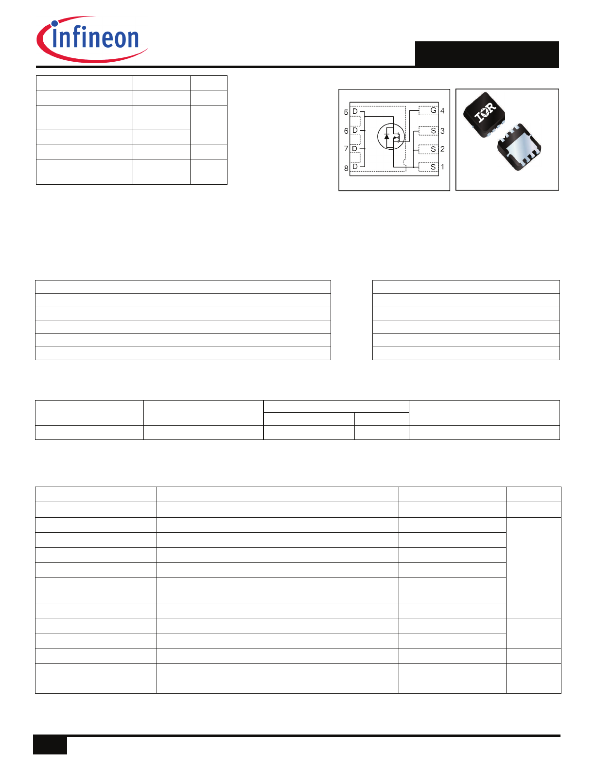
PQFN 3.3X3.3 mm
S
G
S
S
D
D
D
D
D
1
2016-2-23
IRFHM8228PbF
2
2016-2-23
Parameter Typ.
Max.
Units
R
JC
(Bottom) Junction-to-Case –––
3.7
R
JC
(Top)
Junction-to-Case –––
41
°C/W
R
JA
Junction-to-Ambient –––
44
R
JA
(<10s)
Junction-to-Ambient –––
29
Thermal Resistance
Avalanche Characteristics
Parameter
Typ.
Max.
Units
E
AS
Single Pulse Avalanche Energy
–––
50
mJ
D
S
G
Static @ T
J
= 25°C (unless otherwise specified)
Parameter Min.
Typ.
Max.
Units
Conditions
BV
DSS
Drain-to-Source Breakdown Voltage
25
–––
–––
V
V
GS
= 0V, I
D
= 250µA
BV
DSS
/
T
J
Breakdown Voltage Temp. Coefficient
–––
18
––– mV/°C Reference to 25°C, I
D
= 1mA
R
DS(on)
Static Drain-to-Source On-Resistance
–––
4.2
5.2
m
V
GS
= 10V, I
D
= 20A
––– 6.7 8.7
V
GS
= 4.5V, I
D
= 16A
V
GS(th)
Gate Threshold Voltage
1.35
1.8
2.35
V
V
DS
= V
GS
, I
D
= 25µA
V
GS(th)
Gate Threshold Voltage Coefficient
–––
-6.6
––– mV/°C
I
DSS
Drain-to-Source Leakage Current
–––
–––
1.0
V
DS
= 20V, V
GS
= 0V
––– ––– 150
V
DS
= 20V, V
GS
= 0V, T
J
= 125°C
I
GSS
Gate-to-Source Forward Leakage –––
–––
100
nA
V
GS
= 20V
Gate-to-Source Reverse Leakage
–––
–––
-100
V
GS
= -20V
gfs Forward
Transconductance
63
–––
–––
S
V
DS
= 10V, I
D
= 20A
Q
g
Total Gate Charge
–––
18
–––
nC V
GS
= 10V, V
DS
= 13V, I
D
= 20A
Q
g
Total Gate Charge
–––
9.0
14
Q
gs1
Pre-Vth Gate-to-Source Charge
–––
2.7
–––
V
DS
= 13V
Q
gs2
Post-Vth Gate-to-Source Charge
–––
1.0
–––
nC V
GS
= 4.5V
Q
gd
Gate-to-Drain Charge
–––
3.1
–––
I
D
= 20A
Q
godr
Gate Charge Overdrive
–––
2.2
–––
Q
sw
Switch Charge (Q
gs2
+ Q
gd
) –––
4.1
–––
Q
oss
Output Charge
–––
9.7
–––
nC V
DS
= 16V, V
GS
= 0V
R
G
Gate Resistance
–––
1.7
–––
t
d(on)
Turn-On Delay Time
–––
11
–––
V
DD
= 13V, V
GS
= 4.5V
t
r
Rise Time
–––
22
–––
ns I
D
= 20A
t
d(off)
Turn-Off Delay Time
–––
13
–––
R
G
=1.8
t
f
Fall Time
–––
6.2
–––
C
iss
Input Capacitance
–––
1667
–––
V
GS
= 0V
C
oss
Output Capacitance
–––
456
–––
pF V
DS
= 10V
C
rss
Reverse Transfer Capacitance
–––
195
–––
ƒ = 1.0MHz
µA
Diode Characteristics
Parameter
Min. Typ. Max. Units
Conditions
I
S
Continuous Source Current
––– ––– 25
A
MOSFET symbol
(Body Diode)
showing the
I
SM
Pulsed Source Current
––– ––– 260
integral reverse
(Body Diode)
p-n junction diode.
V
SD
Diode Forward Voltage
––– ––– 1.0
V T
J
= 25°C, I
S
= 20A, V
GS
= 0V
t
rr
Reverse Recovery Time
–––
14
21
ns T
J
= 25°C, I
F
= 20A, V
DD
= 13V
Q
rr
Reverse Recovery Charge
–––
10
15
nC di/dt = 260A/µs
IRFHM8228PbF
3
2016-2-23
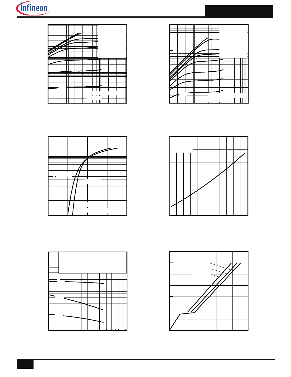
Fig 1. Typical Output Characteristics
Fig 4. Normalized On-Resistance vs. Temperature
1
10
100
VDS, Drain-to-Source Voltage (V)
100
1000
10000
C
, C
ap
ac
ita
nc
e
(p
F
)
VGS = 0V, f = 1 MHZ
Ciss = Cgs + Cgd, C ds SHORTED
Crss = Cgd
Coss = Cds + Cgd
Coss
Crss
Ciss
0
5
10
15
20
25
QG, Total Gate Charge (nC)
0.0
2.0
4.0
6.0
8.0
10.0
12.0
14.0
V
G
S
, G
at
e-
to
-S
ou
rc
e
V
ol
ta
ge
(
V
)
VDS= 20V
VDS= 13V
VDS= 5.0V
ID= 20A
Fig 5. Typical Capacitance vs. Drain-to-Source Voltage
Fig 6. Typical Gate Charge vs. Gate-to-Source Voltage
Fig 3. Typical Transfer Characteristics
0.1
1
10
100
VDS, Drain-to-Source Voltage (V)
1
10
100
1000
I D
, D
ra
in
-t
o
-S
ou
rc
e
C
ur
re
nt
(
A
)
2.5V
60µs PULSE WIDTH
Tj = 150°C
VGS
TOP 10V
7.0V
4.5V
4.0V
3.5V
3.0V
2.75V
BOTTOM
2.5V
-60 -40 -20 0 20 40 60 80 100 120 140 160
TJ , Junction Temperature (°C)
0.6
0.8
1.0
1.2
1.4
1.6
1.8
R
D
S
(o
n)
,
D
ra
in
-t
o-
S
ou
rc
e
O
n
R
es
is
ta
nc
e
(
N
or
m
al
iz
ed
)
ID = 20A
VGS = 10V
Fig 2. Typical Output Characteristics
0.1
1
10
100
VDS, Drain-to-Source Voltage (V)
0.01
0.1
1
10
100
1000
I D
, D
ra
in
-t
o-
S
ou
rc
e
C
ur
re
nt
(
A
)
VGS
TOP 10V
7.0V
4.5V
4.0V
3.5V
3.0V
2.75V
BOTTOM
2.5V
60µs PULSE WIDTH
Tj = 25°C
2.5V
0
2
4
6
8
VGS, Gate-to-Source Voltage (V)
0.1
1
10
100
1000
I D
, D
ra
in
-t
o-
S
ou
rc
e
C
ur
re
nt
(A
)
TJ = 25°C
TJ = 150°C
VDS = 10V
60µs PULSE WIDTH
IRFHM8228PbF
4
2016-2-23
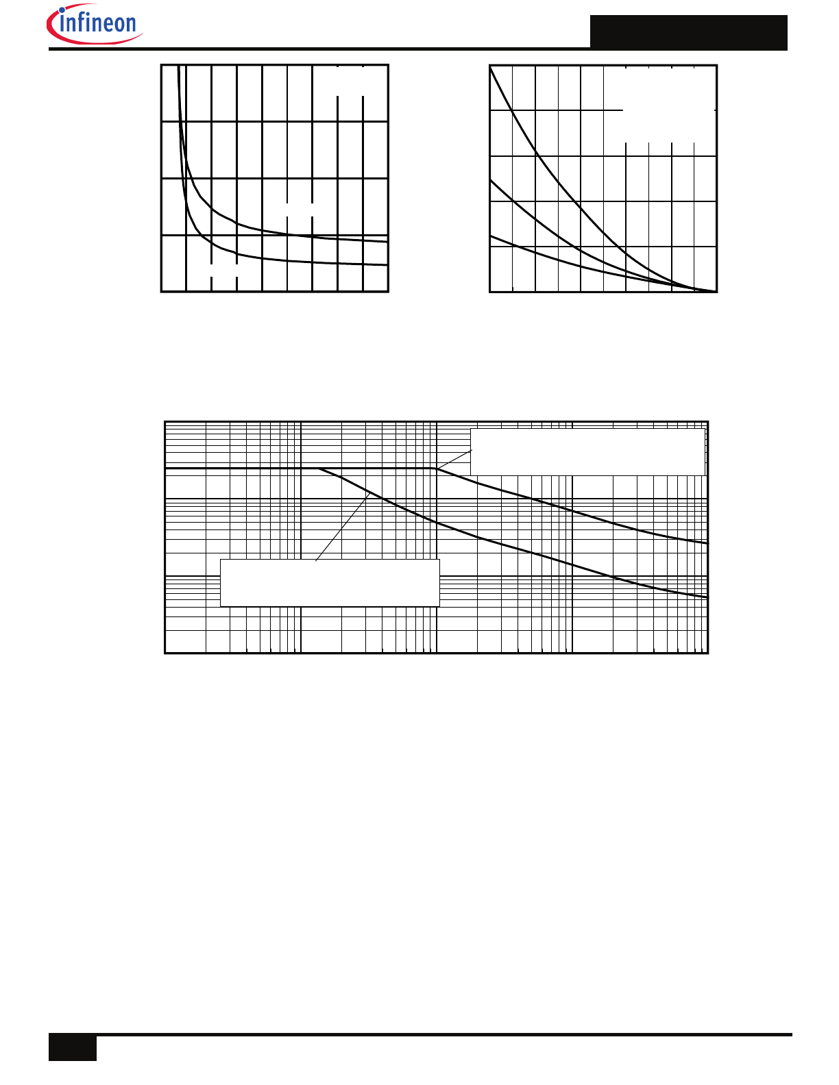
Fig 8. Maximum Safe Operating Area
Fig 11. Maximum Effective Transient Thermal Impedance, Junction-to-Case
0.0
0.4
0.8
1.2
1.6
2.0
VSD, Source-to-Drain Voltage (V)
0.1
1
10
100
1000
I S
D
, R
ev
er
se
D
ra
in
C
ur
re
nt
(
A
)
TJ = 25°C
TJ = 150°C
VGS = 0V
25
50
75
100
125
150
TC , Case Temperature (°C)
0
10
20
30
40
50
60
70
I D
,
D
ra
in
C
ur
re
nt
(
A
)
Limited by source
bonding technology
Fig 7. Typical Source-Drain Diode Forward Voltage
1E-006
1E-005
0.0001
0.001
0.01
0.1
1
t1 , Rectangular Pulse Duration (sec)
0.001
0.01
0.1
1
10
T
he
rma
l R
es
po
ns
e
(
Z
th
JC
)
°
C
/W
0.20
0.10
D = 0.50
0.02
0.01
0.05
SINGLE PULSE
( THERMAL RESPONSE )
Notes:
1. Duty Factor D = t1/t2
2. Peak Tj = P dm x Zthjc + Tc
Fig 9. Maximum Drain Current vs. Case Temperature
Fig 10. Drain-to–Source Breakdown Voltage
-75 -50 -25
0
25
50
75 100 125 150
TJ , Temperature ( °C )
0.5
1.0
1.5
2.0
2.5
3.0
V
G
S
(t
h)
, G
at
e
th
re
sh
ol
d
V
ol
ta
ge
(
V
)
ID = 25µA
ID = 250µA
ID = 1.0mA
ID = 1.0A
0.1
1
10
100
VDS, Drain-to-Source Voltage (V)
0.01
0.1
1
10
100
1000
I D
,
D
ra
in
-t
o-
S
ou
rc
e
C
ur
re
nt
(
A
)
Tc = 25°C
Tj = 150°C
Single Pulse
10msec
1msec
OPERATION IN THIS AREA
LIMITED BY R DS(on)
100µsec
DC
Limited by source bonding
technology
IRFHM8228PbF
5
2016-2-23
2
4
6
8
10
12
14
16
18
20
VGS, Gate -to -Source Voltage (V)
2
6
10
14
18
R
D
S
(o
n)
,
D
ra
in
-t
o
-S
ou
rc
e
O
n
R
e
si
st
an
ce
(
m
)
ID = 20A
TJ = 25°C
TJ = 125°C
Fig 12. On-Resistance vs. Gate Voltage
Fig 13. Maximum Avalanche Energy vs. Drain Current
Fig 14. Single Avalanche Event: Pulse Current vs. Pulse Width
25
50
75
100
125
150
Starting TJ , Junction Temperature (°C)
0
40
80
120
160
200
E
A
S
,
S
in
gl
e
P
ul
se
A
va
la
nc
he
E
ne
rg
y
(m
J)
ID
TOP 4.4A
9.2A
BOTTOM 20A
1.0E-06
1.0E-05
1.0E-04
1.0E-03
1.0E-02
tav (sec)
0.1
1
10
100
A
va
la
nc
he
C
ur
re
nt
(
A
)
Allowed avalanche Current vs avalanche
pulsewidth, tav, assuming j = 25°C and
Tstart = 125°C.
Allowed avalanche Current vs avalanche
pulsewidth, tav, assuming Tj = 125°C and
Tstart =25°C (Single Pulse)
IRFHM8228PbF
6
2016-2-23
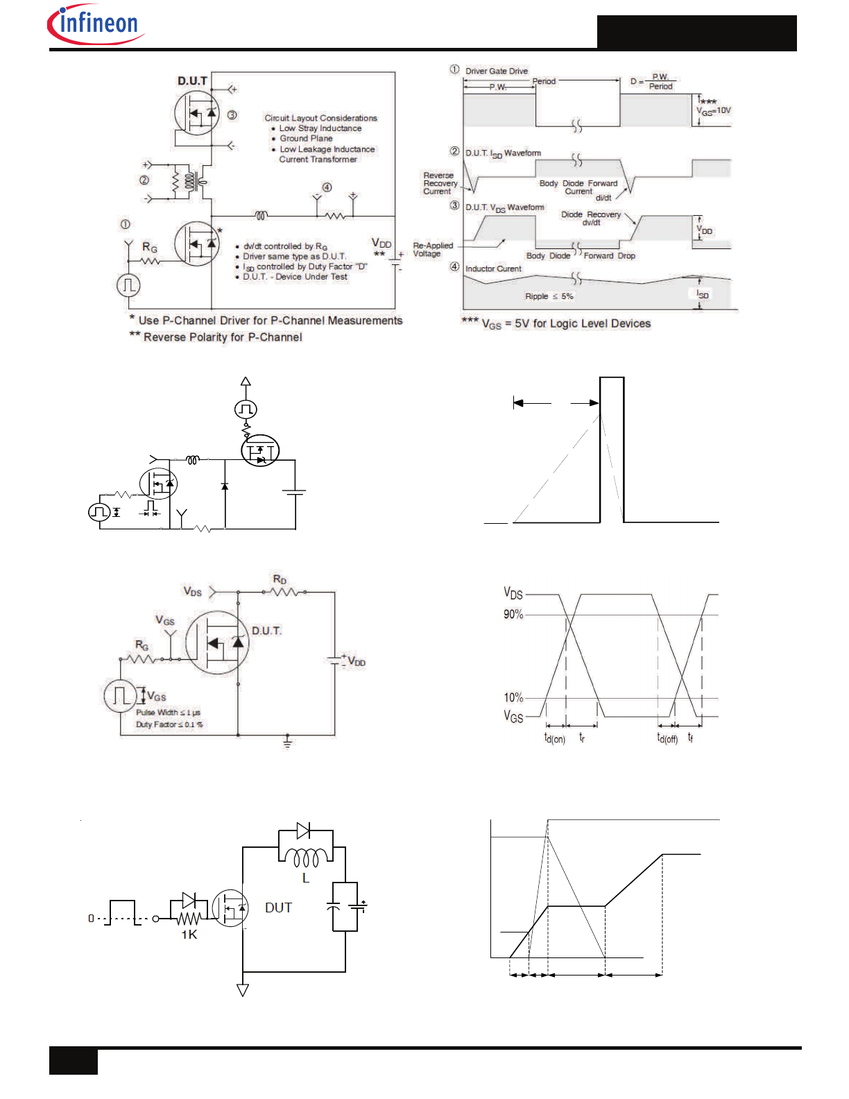
Fig 15. Peak Diode Recovery dv/dt Test Circuit for N-Channel HEXFET
®
Power MOSFETs
Fig 18a. Gate Charge Test Circuit
Vds
Vgs
Id
Vgs(th)
Qgs1 Qgs2
Qgd
Qgodr
Fig 18b. Gate Charge Waveform
Fig 16a. Unclamped Inductive Test Circuit
R G
I
AS
0.01
tp
D.U.T
L
VDS
+
- VDD
DRIVER
A
15V
20V
tp
V
(BR)DSS
I
AS
Fig 16b. Unclamped Inductive Waveforms
Fig 17a. Switching Time Test Circuit
Fig 17b. Switching Time Waveforms
VDD
IRFHM8228PbF
7
2016-2-23
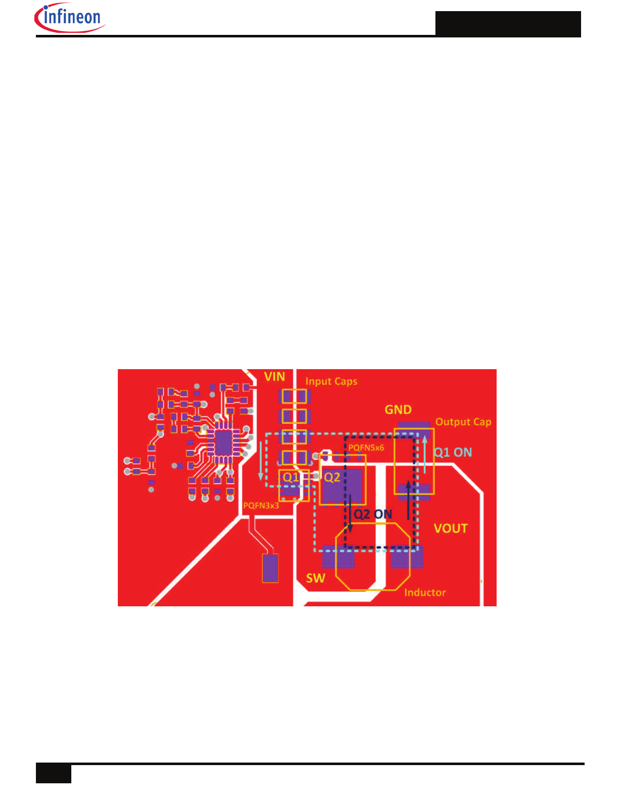
The typical application topology for this product is the synchronous buck converter. These converters operate at high
frequencies (typically around 400 kHz). During turn-on and turn-off switching cycles, the high di/dt currents circulating in
the parasitic elements of the circuit induce high voltage ringing which may exceed the device rating and lead to
undesirable effects. One of the major contributors to the increase in parasitics is the PCB power circuit inductance.
This section introduces a simple guideline that mitigates the effect of these parasitics on the performance of the circuit
and provides reliable operation of the devices.
To reduce high frequency switching noise and the effects of Electromagnetic Interference (EMI) when the control
MOSFET (Q1) is turned on, the layout shown in Figure 19 is recommended. The input bypass capacitors, control
MOSFET and output capacitors are placed in a tight loop to minimize parasitic inductance which in turn lowers the
amplitude of the switch node ringing, and minimizes exposure of the MOSFETs to repetitive avalanche conditions.
Fig 19. Placement and Layout Guidelines
Placement and Layout Guidelines
IRFHM8228PbF
8
2016-2-23
For more information on board mounting, including footprint and stencil recommendation, please refer to application note
AN-1136:
http://www.irf.com/technical-info/appnotes/an-1136.pdf
For more information on package inspection techniques, please refer to application note AN-1154:
http://www.irf.com/technical-info/appnotes/an-1154.pdf
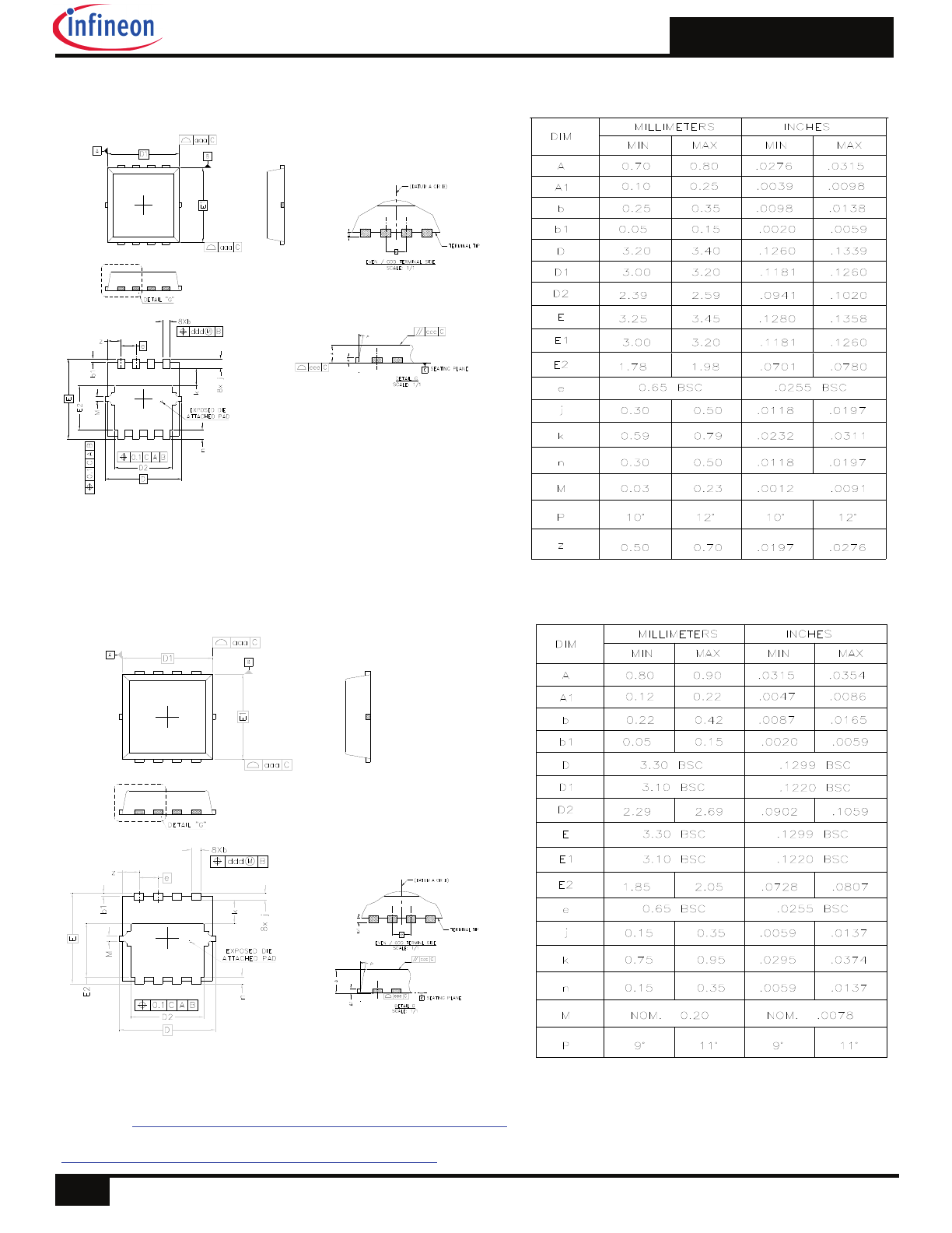
PQFN 3.3 x 3.3 Outline “C” Package Details
PQFN 3.3 x 3.3 Outline “G” Package Details
5
8
7
6
#1
3
2
4
#1
2
3
4
8
7
6
5
5
8
7
6
1
3
2
4
1
2
3
4
8
7
6
5
IRFHM8228PbF
9
2016-2-23
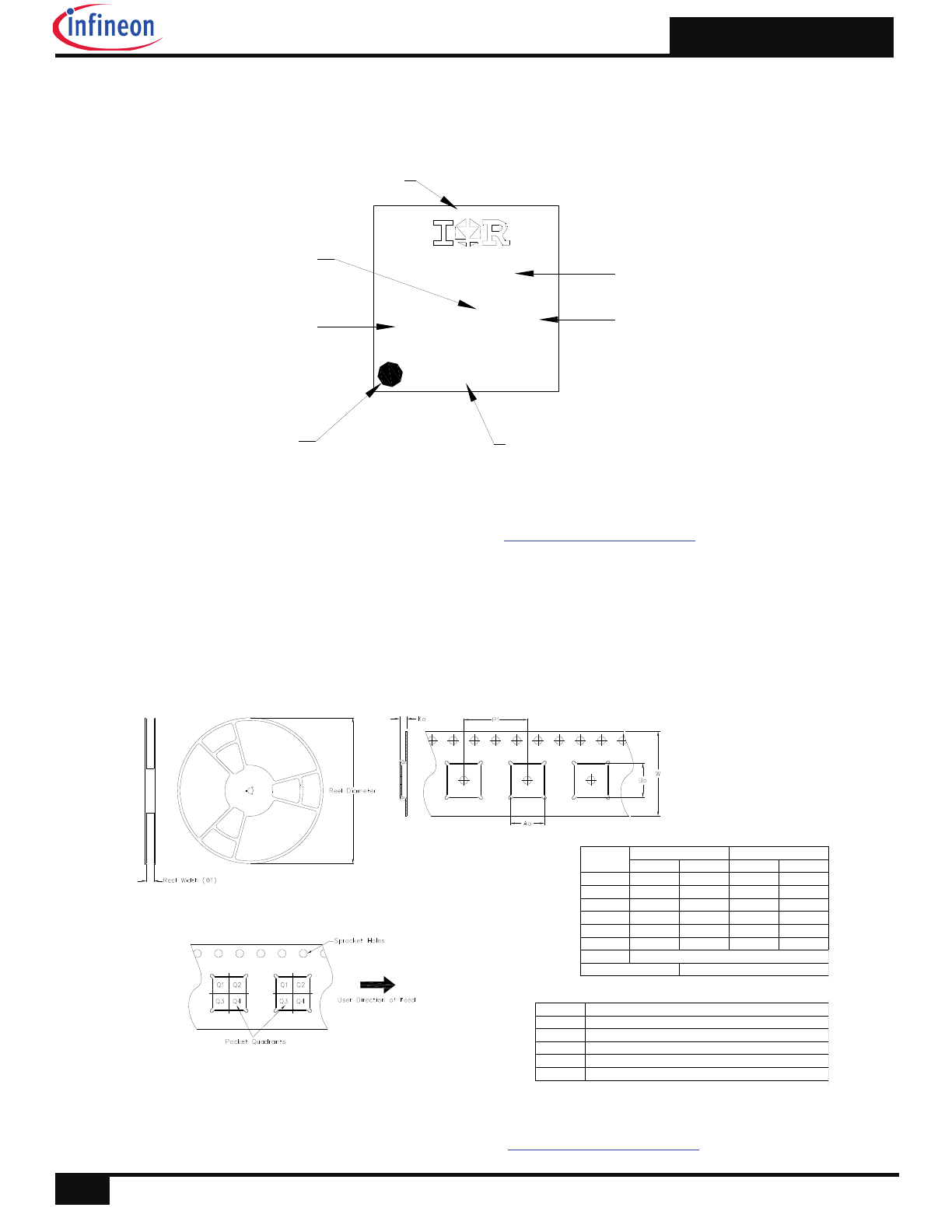
PQFN 3.3mm x 3.3mm Outline Tape and Reel
Bo
W
P1
Ao
Ko
CODE
TAPE DIMENSIONS
REEL DIMENSIONS
QUADRANT ASSIGNMENTS FOR PIN 1 ORIENTATION IN TAPE
Dimension design to accommodate the component width
Dimension design to accommodate the component lenght
Dimension design to accommodate the component thickness
Pitch between successive cavity centers
Overall width of the carrier tape
Bo
W
P1
Ao
Ko
DIMENSION (MM)
CODE
MIN
MAX
DIMENSION (INCH)
MIN
MAX
3.50
3.70
.138
.146
1.10
1.30
7.90
8.10
.043
.051
11.80
12.20
.311
.319
12.30
12.50
.465
.480
.484
.492
3.50
3.70
.138
.146
DESCRIPTION
W1
Qty
4000
Reel Diameter
13 Inches
Note: For the most current drawing please refer to IR website at
http://www.irf.com/package/
PQFN 3.3mm x 3.3mm Outline Part Marking
Note: For the most current drawing please refer to IR website at
http://www.irf.com/package/
XXXX
?YWW?
XXXXX
INTERNATIONAL
RECTIFIER LOGO
PART NUMBER
MARKING CODE
(Per Marking Spec)
ASSEMBLY
SITE CODE
(Per SCOP 200-002)
DATE CODE
LOT CODE
(Eng Mode - Min last 4 digits of EATI#)
(Prod Mode - 4 digits of SPN code)
PIN 1
IDENTIFIER
IRFHM8228PbF
10
2016-2-23
Qualification Information
†
Qualification Level
Moisture Sensitivity Level
PQFN 3.3mm x 3.3mm
MSL1
(per JEDEC J-STD-020D
††
)
RoHS Compliant
Yes
Consumer
††
(per JEDEC JESD47F
†††
guidelines)
†
Qualification standards can be found at International Rectifier’s web site:
http://www.irf.com/product-info/reliability
†† Higher qualification ratings may be available should the user have such requirements. Please contact your
International Rectifier representative for further information:
http://www.irf.com/whoto-call/salesrep/
††† Applicable version of JEDEC standard at the time of product release.
Notes:
Repetitive rating; pulse width limited by max. junction temperature.
Starting T
J
= 25°C, L = 0.25mH, R
G
= 50
, I
AS
= 20A.
Pulse width
400µs; duty cycle 2%.
R
is measured at T
J
of approximately 90°C.
When mounted on 1 inch square 2 oz copper pad on 1.5x1.5 in. board of FR-4 material. Please refer to AN-994
for more details:
http://www.irf.com/technical-info/appnotes/an-994.pdf
Calculated continuous current based on maximum allowable junction temperature.
Current is limited to 25A by source bonding technology.