
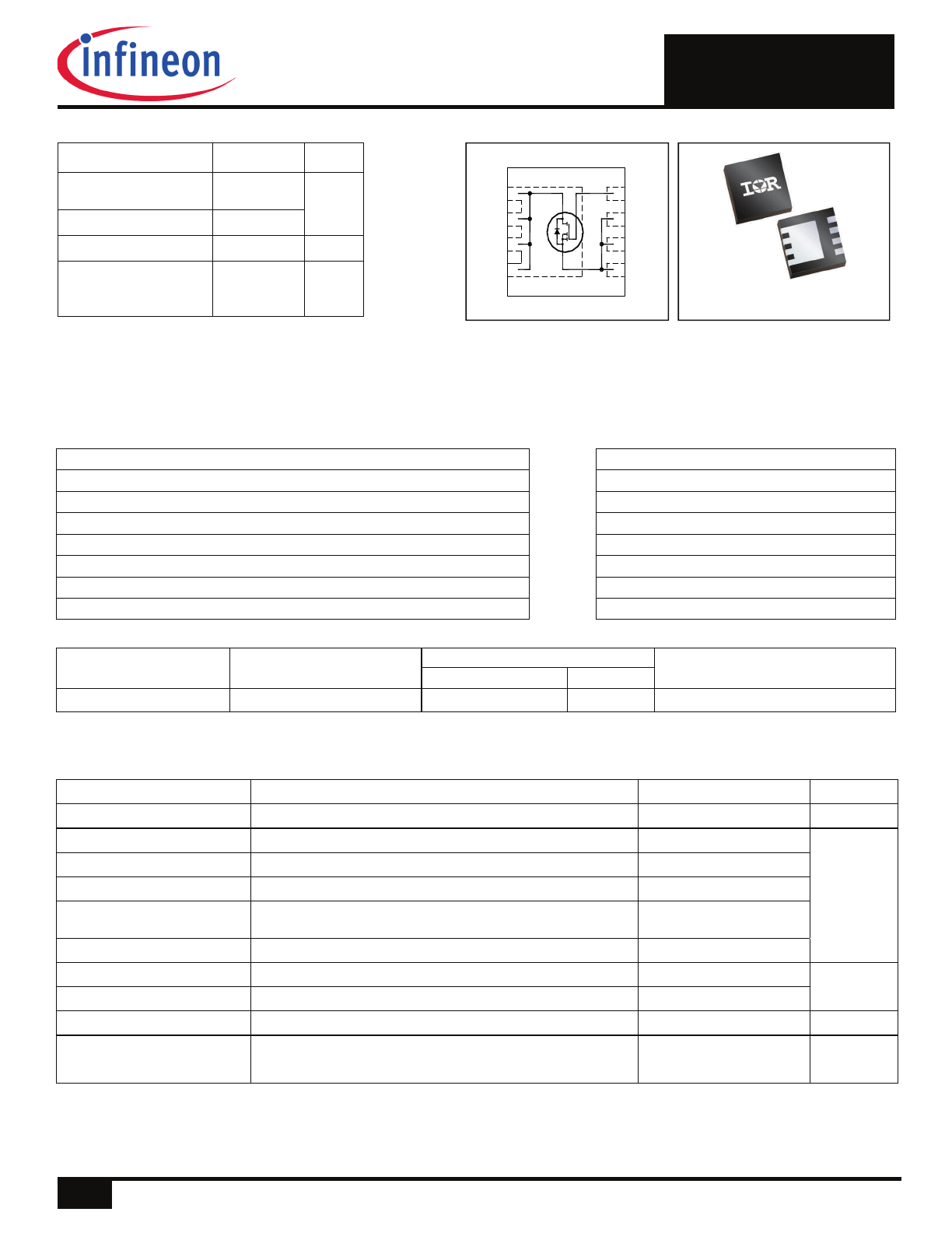
Fast
IR
FET™
IRFHM4234TRPbF
HEXFET
®
Power MOSFET
Base part number
Package Type
Standard Pack
Form
Quantity
IRFHM4234PbF
PQFN 3.3mm x 3.3mm
Tape and Reel
4000
IRFHM4234TRPbF
Orderable Part Number
V
DSS
25
V
R
DS(on)
max
(@ V
GS
= 10V)
4.4
(@ V
GS
= 4.5V)
7.1
Qg
(typical)
8.2
nC
I
D
(@T
C (Bottom)
= 25°C)
60 A
m
Features
Benefits
Low R
DSon
(<4.4 m
)
Lower Conduction Losses
Low Thermal Resistance to PCB (<4.4°C/W)
Enable better Thermal Dissipation
Low Profile (<0.9 mm)
results in Increased Power Density
Industry-Standard Pinout
Multi-Vendor Compatibility
Compatible with Existing Surface Mount Techniques
Easier Manufacturing
RoHS Compliant, Halogen-Free
Environmentally Friendlier
MSL1, Industrial Qualification
Increased Reliability
Low Charge (typical 8.2 nC)
Low Switching Losses
Notes through are on page 9
Absolute Maximum Ratings
Parameter Max.
Units
V
GS
Gate-to-Source Voltage
± 20
V
I
D
@ T
A
= 25°C
Continuous Drain Current, V
GS
@ 10V
20
A
I
D
@ T
C(Bottom)
= 25°C
Continuous Drain Current, V
GS
@ 10V
63
I
D
@ T
C(Bottom)
= 100°C
Continuous Drain Current, V
GS
@ 10V
44
I
DM
Pulsed Drain Current 270
P
D
@T
A
= 25°C
Power Dissipation 2.8
W
P
D
@T
C(Bottom)
= 25°C
Power Dissipation
28
Linear Derating Factor
0.022
W/°C
T
J
Operating Junction and
-55 to + 150
°C
T
STG
Storage Temperature Range
I
D
@ T
C
= 25°C
Continuous Drain Current, V
GS
@ 10V
(Source Bonding Technology Limited)
60
Applications
Control MOSFET for synchronous buck converter
PQFN 3.3 x 3.3 mm
Top View
3
2
1
8
7
6
5
4
D
D
D
D
S
S
S
G
1
2016-2-26
IRFHM4234TRPbF
2
2016-2-26
D
S
G
Static @ T
J
= 25°C (unless otherwise specified)
Parameter Min.
Typ.
Max.
Units
Conditions
BV
DSS
Drain-to-Source Breakdown Voltage
25
–––
–––
V
V
GS
= 0V, I
D
= 250µA
BV
DSS
/
T
J
Breakdown Voltage Temp. Coefficient
–––
21
––– mV/°C Reference to 25°C, I
D
= 1mA
R
DS(on)
Static Drain-to-Source On-Resistance
–––
3.5
4.4
m
V
GS
= 10V, I
D
= 30A
––– 5.6 7.1
V
GS
= 4.5V, I
D
= 30A
V
GS(th)
Gate Threshold Voltage
1.1
1.6
2.1
V
V
GS(th)
Gate Threshold Voltage Coefficient
–––
-5.5
––– mV/°C
I
DSS
Drain-to-Source Leakage Current
–––
–––
1.0
µA V
DS
= 20V, V
GS
= 0V
I
GSS
Gate-to-Source Forward Leakage
–––
–––
100
nA
V
GS
= 20V
Gate-to-Source Reverse Leakage
–––
–––
-100
V
GS
= -20V
gfs Forward
Transconductance
60
–––
–––
S
V
DS
= 5.0V, I
D
= 30A
Q
g
Total Gate Charge
–––
17
–––
nC V
GS
= 10V, V
DS
= 13V, I
D
= 30A
Q
g
Total Gate Charge
–––
8.2
12.3
Q
gs1
Pre-Vth Gate-to-Source Charge
–––
1.6
–––
V
DS
= 13V
Q
gs2
Post-Vth Gate-to-Source Charge
–––
1.6
–––
nC V
GS
= 4.5V
Q
gd
Gate-to-Drain Charge
–––
3.1
–––
I
D
= 30A
Q
godr
Gate Charge Overdrive
–––
1.9
–––
Q
sw
Switch Charge (Q
gs2
+ Q
gd
) –––
4.7
–––
Q
oss
Output Charge
–––
7.7
–––
nC V
DS
= 16V, V
GS
= 0V
R
G
Gate Resistance
–––
1.8
–––
t
d(on)
Turn-On Delay Time
–––
7.8
–––
V
DD
= 13V, V
GS
= 4.5V
t
r
Rise Time
–––
30
–––
ns I
D
= 30A
t
d(off)
Turn-Off Delay Time
–––
8.0
–––
R
G
=1.8
t
f
Fall Time
–––
5.3
–––
C
iss
Input Capacitance
–––
1011
–––
V
GS
= 0V
C
oss
Output Capacitance
–––
286
–––
pF V
DS
= 13V
C
rss
Reverse Transfer Capacitance
–––
83
–––
ƒ = 1.0MHz
Avalanche Characteristics
Parameter
Typ.
Max.
E
AS
Single Pulse Avalanche Energy
–––
39
I
AR
Avalanche Current
–––
30
Diode Characteristics
Parameter
Min.
Typ.
Max. Units
Conditions
I
S
Continuous Source Current
––– ––– 60
A
MOSFET symbol
(Body Diode)
showing the
I
SM
Pulsed Source Current
––– ––– 270
integral reverse
(Body Diode)
p-n junction diode.
V
SD
Diode Forward Voltage
–––
–––
1.0
V
T
J
= 25°C, I
S
= 30A, V
GS
= 0V
t
rr
Reverse Recovery Time
–––
10
15
ns
T
J
= 25°C, I
F
= 30A, V
DD
= 13V
Q
rr
Reverse Recovery Charge
–––
11
17
nC di/dt = 200A/µs
V
DS
= V
GS
, I
D
= 25µA
Parameter Typ.
Max.
Units
R
JC
(Bottom) Junction-to-Case –––
4.4
R
JC
(Top)
Junction-to-Case –––
40
°C/W
R
JA
Junction-to-Ambient –––
45
R
JA
(<10s)
Junction-to-Ambient –––
31
Thermal Resistance
IRFHM4234TRPbF
3
2016-2-26
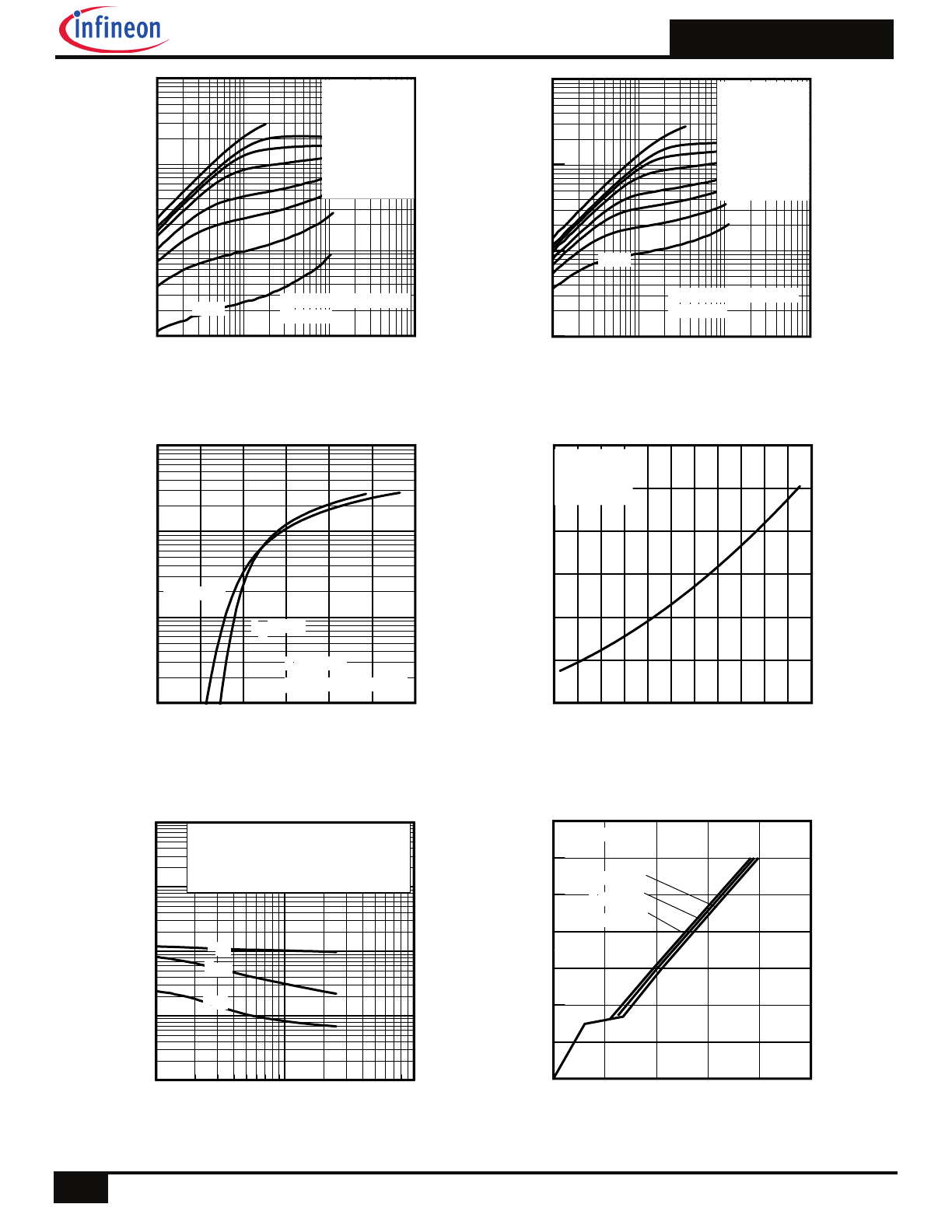
Fig 1. Typical Output Characteristics
0
5
10
15
20
25
QG, Total Gate Charge (nC)
0.0
2.0
4.0
6.0
8.0
10.0
12.0
14.0
V
G
S
, G
at
e-
to
-S
ou
rc
e
V
o
lta
g
e
(V
)
VDS= 20V
VDS= 13V
VDS= 5.0V
ID= 30A
Fig 4. Normalized On-Resistance vs. Temperature
Fig 5. Typical Capacitance vs. Drain-to-Source Voltage
Fig 6. Typical Gate Charge vs. Gate-to-Source Voltage
1
10
100
VDS, Drain-to-Source Voltage (V)
10
100
1000
10000
100000
C
, C
ap
ac
ita
n
ce
(
pF
)
VGS = 0V, f = 1 MHZ
Ciss = Cgs + Cgd, Cds SHORTED
Crss = Cgd
Coss = Cds + Cgd
Coss
Crss
Ciss
Fig 3. Typical Transfer Characteristics
0.1
1
10
100
VDS, Drain-to-Source Voltage (V)
1
10
100
1000
I D
, D
ra
in
-t
o-
S
ou
rc
e
C
ur
re
nt
(
A
)
2.75V
60µs PULSE WIDTH
Tj = 150°C
VGS
TOP
10V
5.0V
4.5V
4.0V
3.5V
3.25V
3.0V
BOTTOM
2.75V
Fig 2. Typical Output Characteristics
0.1
1
10
100
VDS, Drain-to-Source Voltage (V)
1
10
100
1000
I D
, D
ra
in
-t
o-
S
ou
rc
e
C
ur
re
nt
(
A
)
VGS
TOP
10V
5.0V
4.5V
4.0V
3.5V
3.25V
3.0V
BOTTOM
2.75V
60µs PULSE WIDTH
Tj = 25°C
2.75V
1.0
2.0
3.0
4.0
5.0
6.0
7.0
VGS, Gate-to-Source Voltage (V)
1.0
10
100
1000
I D
, D
ra
in
-t
o-
S
ou
rc
e
C
ur
re
nt
(
A
)
TJ = 25°C
TJ = 150°C
VDS = 10V
60µs PULSE WIDTH
-60 -40 -20 0 20 40 60 80 100 120 140 160
TJ , Junction Temperature (°C)
0.6
0.8
1.0
1.2
1.4
1.6
1.8
R
D
S
(o
n)
,
D
ra
in
-t
o-
S
ou
rc
e
O
n
R
e
si
st
an
ce
(
N
o
rm
al
iz
ed
)
ID = 30A
VGS = 10V
IRFHM4234TRPbF
4
2016-2-26
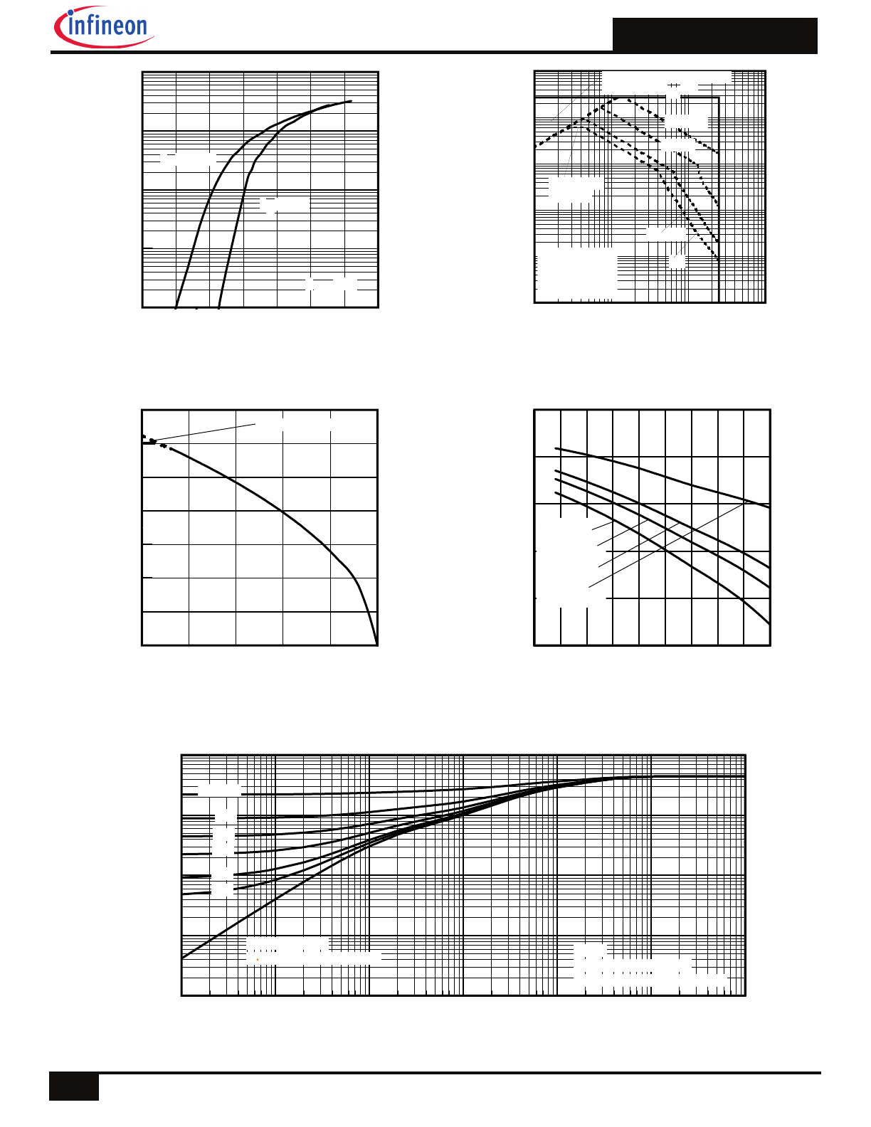
Fig 8. Maximum Safe Operating Area
0.2
0.4
0.6
0.8
1.0
1.2
1.4
1.6
VSD, Source-to-Drain Voltage (V)
0.1
1
10
100
1000
I S
D
, R
ev
er
se
D
ra
in
C
ur
re
nt
(
A
)
TJ = 25°C
TJ = 150°C
VGS = 0V
Fig 7. Typical Source-Drain Diode Forward Voltage
Fig 9. Maximum Drain Current vs. Case Temperature
Fig 10. Drain-to-Source Breakdown Voltage
1E-006
1E-005
0.0001
0.001
0.01
0.1
1
t1 , Rectangular Pulse Duration (sec)
0.001
0.01
0.1
1
10
T
he
rma
l R
e
sp
o
ns
e
(
Z
th
JC
)
°C
/W
0.20
0.10
D = 0.50
0.02
0.01
0.05
SINGLE PULSE
( THERMAL RESPONSE )
Notes:
1. Duty Factor D = t1/t2
2. Peak Tj = P dm x Zthjc + Tc
Fig 11. Maximum Effective Transient Thermal Impedance, Junction-to-Case
-75 -50 -25
0
25
50
75 100 125 150
TJ , Temperature ( °C )
0.8
1.2
1.6
2.0
2.4
2.8
V
G
S
(t
h
),
G
at
e
th
re
sh
ol
d
V
ol
ta
ge
(
V
)
ID = 25µA
ID = 250µA
ID = 1.0mA
ID = 1.0A
25
50
75
100
125
150
TC , Case Temperature (°C)
0
10
20
30
40
50
60
70
I D
,
D
ra
in
C
u
rr
e
nt
(
A
)
Limited by package
0.1
1
10
100
VDS, Drain-to-Source Voltage (V)
0.01
0.1
1
10
100
1000
I D
,
D
ra
in
-t
o-
S
ou
rc
e
C
ur
re
nt
(
A
)
Tc = 25°C
Tj = 150°C
Single Pulse
10msec
1msec
OPERATION IN THIS AREA
LIMITED BY RDS(on)
100µsec
DC
Limited by
package
IRFHM4234TRPbF
5
2016-2-26
2
4
6
8
10
12
14
16
18
20
VGS, Gate -to -Source Voltage (V)
2.0
4.0
6.0
8.0
10.0
R
D
S
(o
n)
,
D
ra
in
-t
o
-S
o
ur
ce
O
n
R
es
is
ta
nc
e
(
m
)
ID = 30A
TJ = 25°C
TJ = 125°C
Fig 12. On– Resistance vs. Gate Voltage
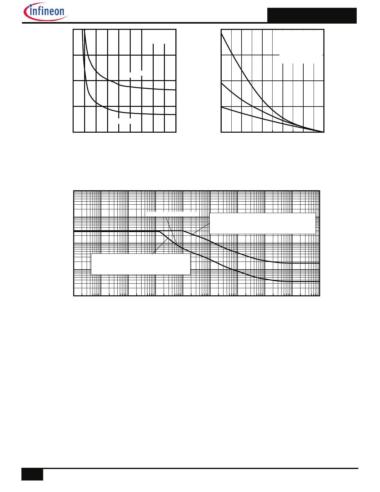
Fig 13. Maximum Avalanche Energy vs. Drain Current
Fig 14. Typical Avalanche Current vs. Pulsewidth
25
50
75
100
125
150
Starting TJ , Junction Temperature (°C)
0
40
80
120
160
E
A
S
,
S
in
g
le
P
ul
se
A
va
la
n
ch
e
E
ne
rg
y
(m
J)
ID
TOP 7.5A
17A
BOTTOM 30A
1.0E-06
1.0E-05
1.0E-04
1.0E-03
1.0E-02
1.0E-01
1.0E+00
1.0E+01
1.0E+02
1.0E+03
tav (sec)
0.1
1
10
100
1000
A
va
la
nc
he
C
ur
re
nt
(
A
)
Duty Cycle = Single Pulse
Allowed avalanche Current vs avalanche
pulsewidth, tav, assuming j = 25°C and
Tstart = 125°C.
Allowed avalanche Current vs avalanche
pulsewidth, tav, assuming Tj = 125°C and
Tstart =25°C (Single Pulse)
IRFHM4234TRPbF
6
2016-2-26
Fig 15. Peak Diode Recovery dv/dt Test Circuit for N-Channel HEXFET
®
Power MOSFETs
Fig 18. Gate Charge Test Circuit
Vds
Vgs
Id
Vgs(th)
Qgs1 Qgs2
Qgd
Qgodr
Fig 19. Gate Charge Waveform
Fig 17a. Switching Time Test Circuit
Fig 17b. Switching Time Waveforms
Fig 16a. Unclamped Inductive Test Circuit
R G
I
AS
0.01
tp
D.U.T
L
VDS
+
- VDD
DRIVER
A
15V
20V
tp
V
(BR)DSS
I
AS
Fig 16b. Unclamped Inductive Waveforms
VDD
IRFHM4234TRPbF
7
2016-2-26
For more information on board mounting, including footprint and stencil recommendation, please refer to application note
AN-1136:
http://www.irf.com/technical-info/appnotes/an-1136.pdf
For more information on package inspection techniques, please refer to application note AN-1154:
http://www.irf.com/technical-info/appnotes/an-1154.pdf
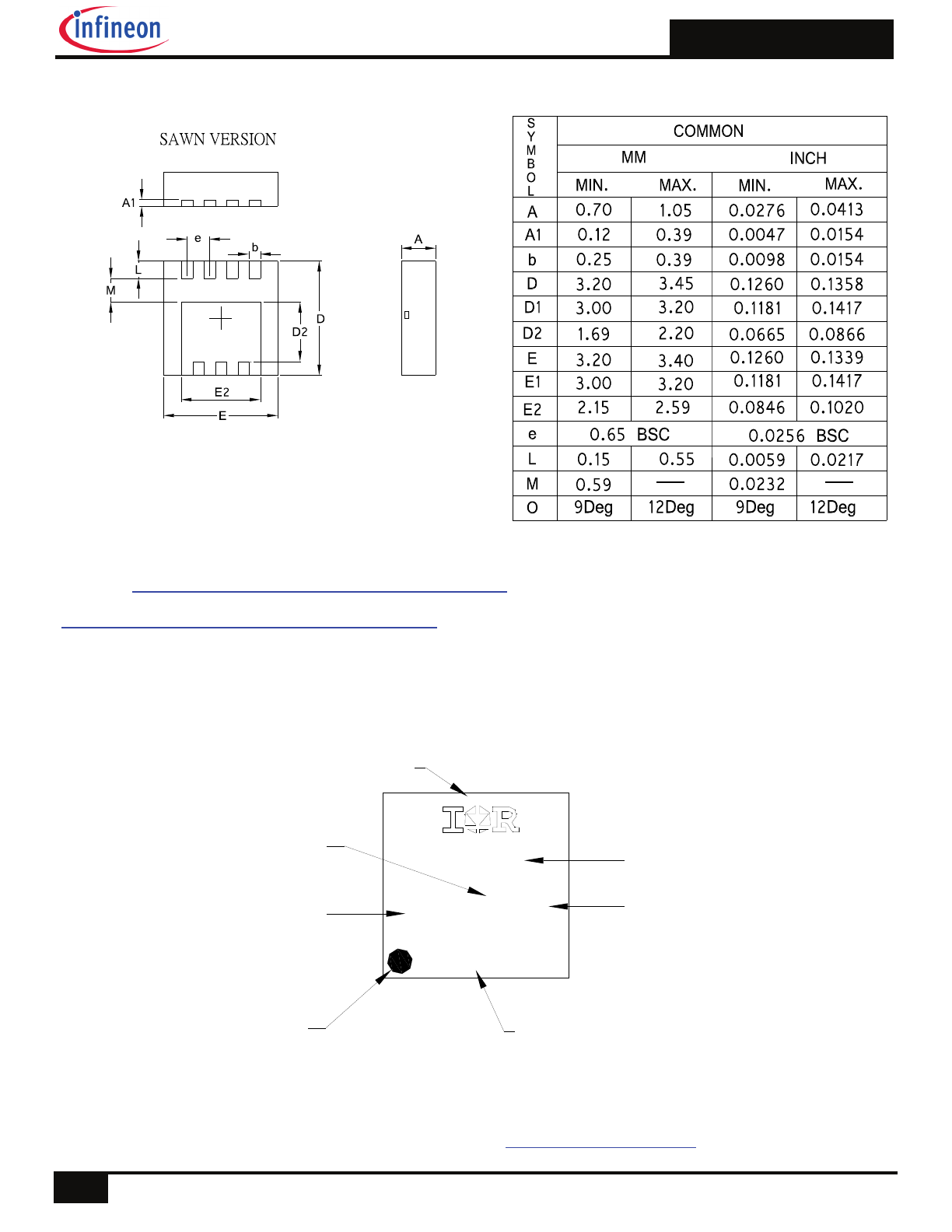
PQFN 3.3 x 3.3 Outline “B” Package Details
PQFN 3.3 x 3.3 Part Marking
XXXX
?YWW?
XXXXX
INTERNATIONAL
RECTIFIER LOGO
PART NUMBER
MARKING CODE
(Per Marking Spec)
ASSEMBLY
SITE CODE
(Per SCOP 200-002)
DATE CODE
LOT CODE
(Eng Mode - Min last 4 digits of EATI#)
(Prod Mode - 4 digits of SPN code)
PIN 1
IDENTIFIER
Note: For the most current drawing please refer to IR website at
http://www.irf.com/package/
IRFHM4234TRPbF
8
2016-2-26
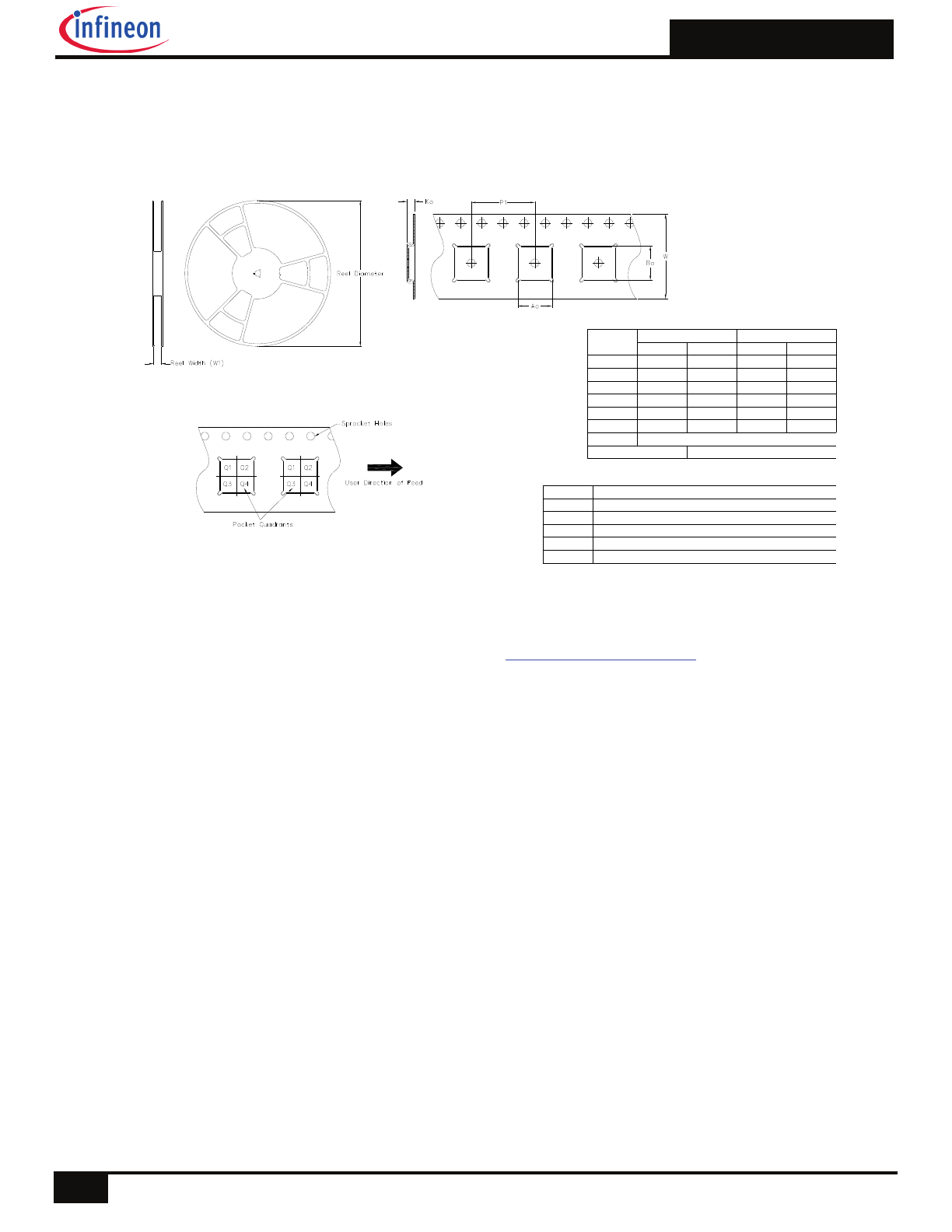
Note: For the most current drawing please refer to IR website at
http://www.irf.com/package/
Bo
W
P1
Ao
Ko
CODE
TAPE DIMENSIONS
REEL DIMENSIONS
QUADRANT ASSIGNMENTS FOR PIN 1 ORIENTATION IN TAPE
Dimension design to accommodate the component width
Dimension design to accommodate the component lenght
Dimension design to accommodate the component thickness
Pitch between successive cavity centers
Overall width of the carrier tape
Bo
W
P1
Ao
Ko
DIMENSION (MM)
CODE
MIN
MAX
DIMENSION (INCH)
MIN
MAX
3.50
3.70
.138
.146
1.10
1.30
7.90
8.10
.043
.051
11.80
12.20
.311
.319
12.30
12.50
.465
.480
.484
.492
3.50
3.70
.138
.146
DESCRIPTION
W1
Qty
4000
Reel Diameter
13 Inches
PQFN 3.3mm x 3.3mm Outline Tape and Reel

IRFHM4234TRPbF
9
2016-2-26
Notes:
Repetitive rating; pulse width limited by max. junction temperature.
Starting T
J
= 25°C, L = 0.087mH, R
G
= 50
, I
AS
= 30A.
Pulse width
400µs; duty cycle 2%.
R
is measured at TJ of approximately 90°C.
When mounted on 1 inch square PCB (FR-4). Please refer to AN-994 for more details:
http://www.irf.com/technical-info/appnotes/an-994.pdf
Calculated continuous current based on maximum allowable junction temperature.
Current is limited to 60A by source bonding technology for 1 inch square FR-4, or 85A for large area 6 oz. copper on
a large area copper Insulated Metal Substrate (IMS).
Qualification Information
†
Qualification Level
Moisture Sensitivity Level
PQFN 3.3mm x 3.3mm
MSL1
(per JEDEC J-STD-020D
††)
RoHS Compliant
Yes
Industrial
(per JEDEC JESD47F
††
guidelines)
† Qualification standards can be found at International Rectifier’s web site:
http://www.irf.com/product-info/reliability
†† Applicable version of JEDEC standard at the time of product release.
IRFHM4234TRPbF
10
2016-2-26
Revision History
Date Comments
6/21/2013
Updated figure 10 ID label from 1.0mA to 1.0A, on page 4.
8/15/2013
Added “FastIRFET™” above the part number, on page 1.
6/6/2014
Updated schematic on page 1.
Updated tape and reel on page 8.
7/24/2014
Updated Id @ Tc 25C from “40A” to “60A”-pg1& 2.
Updated Id @ Tc (bottom) 100c from “40A” to “44A”-pg1.
Updated fig 8 & 9 on page 4.
Updated note 7 on page 9.
2/26/2016
Updated datasheet with corporate template.
Removed package outline “Punched Version” on page 7.
Published by
Infineon Technologies AG
81726 München, Germany
©
Infineon Technologies AG 2015
All Rights Reserved.
IMPORTANT NOTICE
The information given in this document shall in no event be regarded as a guarantee of conditions or characteristics
(“Beschaffenheitsgarantie”). With respect to any examples, hints or any typical values stated herein and/or any
information regarding the application of the product, Infineon Technologies hereby disclaims any and all warranties and
liabilities of any kind, including without limitation warranties of non-infringement of intellectual property rights of any third
party.
In addition, any information given in this document is subject to customer’s compliance with its obligations stated in this
document and any applicable legal requirements, norms and standards concerning customer’s products and any use of
the product of Infineon Technologies in customer’s applications.
The data contained in this document is exclusively intended for technically trained staff. It is the responsibility of
customer’s technical departments to evaluate the suitability of the product for the intended application and the
completeness of the product information given in this document with respect to such application.
For further information on the product, technology, delivery terms and conditions and prices please contact your nearest
Infineon Technologies office (
www.infineon.com
).
WARNINGS
Due to technical requirements products may contain dangerous substances. For information on the types in question
please contact your nearest Infineon Technologies office.
Except as otherwise explicitly approved by Infineon Technologies in a written document signed by authorized
representatives of Infineon Technologies, Infineon Technologies’ products may not be used in any applications where a
failure of the product or any consequences of the use thereof can reasonably be expected to result in personal injury.