
HEXFET
®
Power MOSFET
Notes
through
are on page 10
Applications
l
Synchronous MOSFET for Notebook
Processor Power
l
Synchronous Rectifer MOSFET for Isolated
DC-DC Converters in Networking Systems
Benefits
l
Very low R
DS(ON)
at 4.5V V
GS
l
Low Gate Charge
l
Fully Characterized Avalanche Voltage and
Current
l
100% Tested for R
G
l
Lead-Free (Qualified up to 260°C Reflow)
l
RoHS compliant (Halogen Free)
l
Low Thermal Resistance
l
Large Source Lead for more reliable Soldering
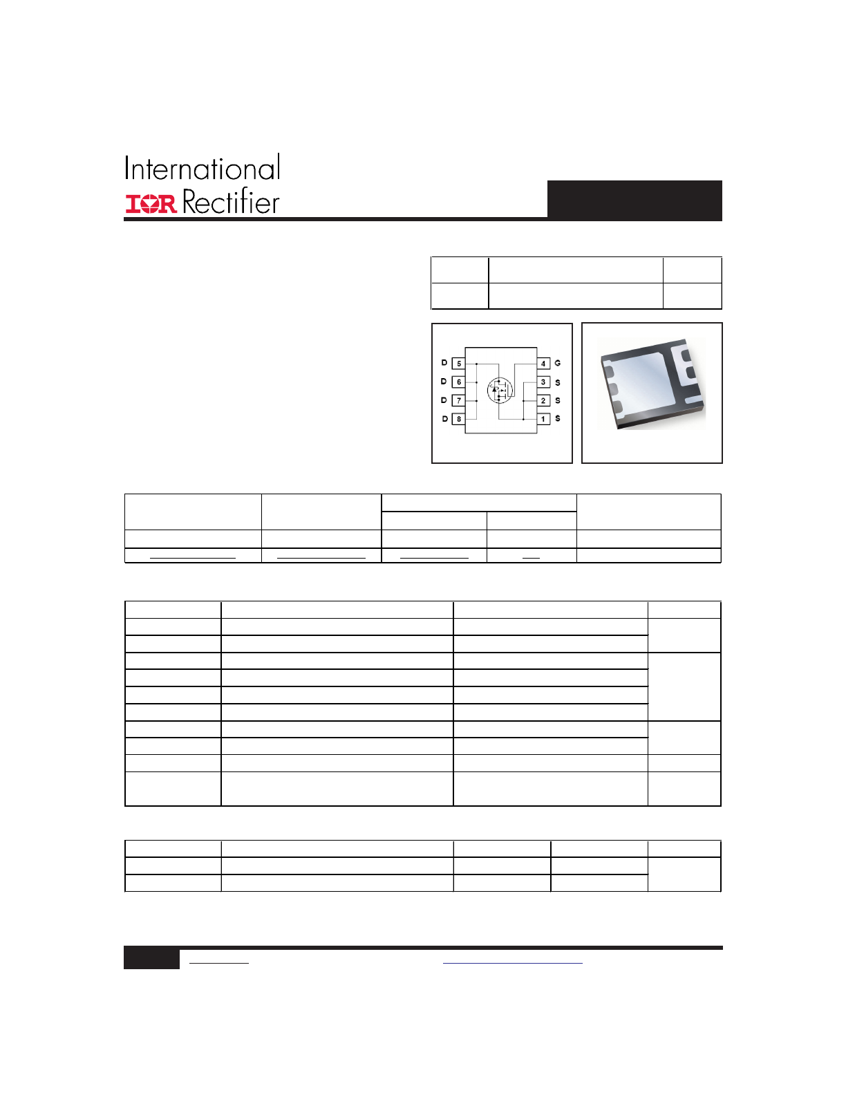
PQFN
D
D
D
D
S
G
S
S
V
DSS
R
DS(on)
max
Qg
30V
3.3m:@V
GS
= 10V 34nC
Absolute Maximum Ratings
Parameter
Units
V
DS
Drain-to-Source Voltage
V
GS
Gate-to-Source Voltage
I
D
@ T
A
= 25°C
Continuous Drain Current, V
GS
@ 10V
I
D
@ T
A
= 70°C
Continuous Drain Current, V
GS
@ 10V
I
D
@ T
C
= 25°C
Continuous Drain Current, V
GS
@ 10V
I
DM
Pulsed Drain Current
c
P
D
@T
A
= 25°C
Power Dissipation
g
P
D
@T
A
= 70°C
Power Dissipation
g
Linear Derating Factor
g
W/°C
T
J
Operating Junction and
T
STG
Storage Temperature Range
Thermal Resistance
Parameter
Typ.
Max.
Units
R
θJC
Junction-to-Case
f
–––
2.2
R
θJA
Junction-to-Ambient
g
–––
37
°C/W
°C
W
A
V
Max.
25
104
200
± 20
30
20
-55 to + 150
3.4
0.03
2.2
IRFH7932PbF
1
www.irf.com
©
2014 International Rectifier
Submit Datasheet Feedback
August 11, 2014
Form
Quantity
IRFH7932TRPbF
PQFN 5mm x 6mm
Tape and Reel
4000
IRFH7932TR2PbF
PQFN 5mm x 6mm
Tape and Reel
400
EOL notice # 259
Orderable part number
Package Type
Standard Pack
Note
2
www.irf.com
©
2014 International Rectifier
Submit Datasheet Feedback
August 11, 2014
IRFH7932PbF
S
D
G
Static @ T
J
= 25°C (unless otherwise specified)
Parameter
Min. Typ. Max. Units
BV
DSS
Drain-to-Source Breakdown Voltage
30
–––
–––
V
∆ΒV
DSS
/
∆T
J
Breakdown Voltage Temp. Coefficient
–––
0.021
–––
V/°C
R
DS(on)
Static Drain-to-Source On-Resistance
–––
2.5
3.3
–––
3.3
3.9
V
GS(th)
Gate Threshold Voltage
1.35
1.8
2.35
V
∆V
GS(th)
Gate Threshold Voltage Coefficient
–––
-5.9
––– mV/°C
I
DSS
Drain-to-Source Leakage Current
–––
–––
1.0
–––
–––
150
I
GSS
Gate-to-Source Forward Leakage
–––
–––
100
Gate-to-Source Reverse Leakage
–––
–––
-100
gfs
Forward Transconductance
59
–––
–––
S
Q
g
Total Gate Charge
–––
34
51
Q
gs1
Pre-Vth Gate-to-Source Charge
–––
7.9
–––
Q
gs2
Post-Vth Gate-to-Source Charge
–––
3.6
–––
Q
gd
Gate-to-Drain Charge
–––
11
–––
Q
godr
Gate Charge Overdrive
–––
12
–––
See Fig.17 & 18
Q
sw
Switch Charge (Q
gs2
+ Q
gd
)
–––
15
–––
Q
oss
Output Charge
–––
19
–––
nC
R
G
Gate Resistance
–––
0.7
–––
Ω
t
d(on)
Turn-On Delay Time
–––
20
–––
t
r
Rise Time
–––
48
–––
t
d(off)
Turn-Off Delay Time
–––
23
–––
t
f
Fall Time
–––
20
–––
C
iss
Input Capacitance
–––
4270
–––
C
oss
Output Capacitance
–––
830
–––
C
rss
Reverse Transfer Capacitance
–––
420
–––
Avalanche Characteristics
Parameter
Units
E
AS
Single Pulse Avalanche Energy
d
mJ
I
AR
Avalanche Current
c
A
Diode Characteristics
Parameter
Min. Typ. Max. Units
I
S
Continuous Source Current
(Body Diode)
I
SM
Pulsed Source Current
(Body Diode)
c
V
SD
Diode Forward Voltage
–––
–––
1.0
V
t
rr
Reverse Recovery Time
–––
21
32
ns
Q
rr
Reverse Recovery Charge
–––
33
50
nC
t
on
Forward Turn-On Time
Intrinsic turn-on time is negligible (turn-on is dominated by LS+LD)
–––
I
D
= 20A
V
GS
= 0V
V
DS
= 15V
20
ƒ = 1.0MHz
V
GS
= 4.5V, I
D
= 20A
e
V
GS
= 4.5V
Typ.
–––
R
G
=1.8
Ω
V
DS
= 15V, I
D
= 20A
V
DS
= 24V, V
GS
= 0V, T
J
= 125°C
m
Ω
V
DS
= 24V, V
GS
= 0V
V
DS
= 15V
T
J
= 25°C, I
F
= 20A, V
DD
= 15V
di/dt = 300A/µs
eSee Fig.16
T
J
= 25°C, I
S
= 20A, V
GS
= 0V
e
showing the
integral reverse
p-n junction diode.
V
GS
= 20V
V
GS
= -20V
MOSFET symbol
V
DS
= 16V, V
GS
= 0V
V
DD
= 15V, V
GS
= 4.5V
I
D
= 20A
See Fig.15
Max.
16
Conditions
V
GS
= 0V, I
D
= 250µA
Reference to 25°C, I
D
= 1mA
V
GS
= 10V, I
D
= 25A
e
–––
–––
–––
–––
A
4.2
200
V
DS
= V
GS
, I
D
= 100µA
ns
pF
nC
nA
µA
Conditions
3
www.irf.com
©
2014 International Rectifier
Submit Datasheet Feedback
August 11, 2014
IRFH7932PbF
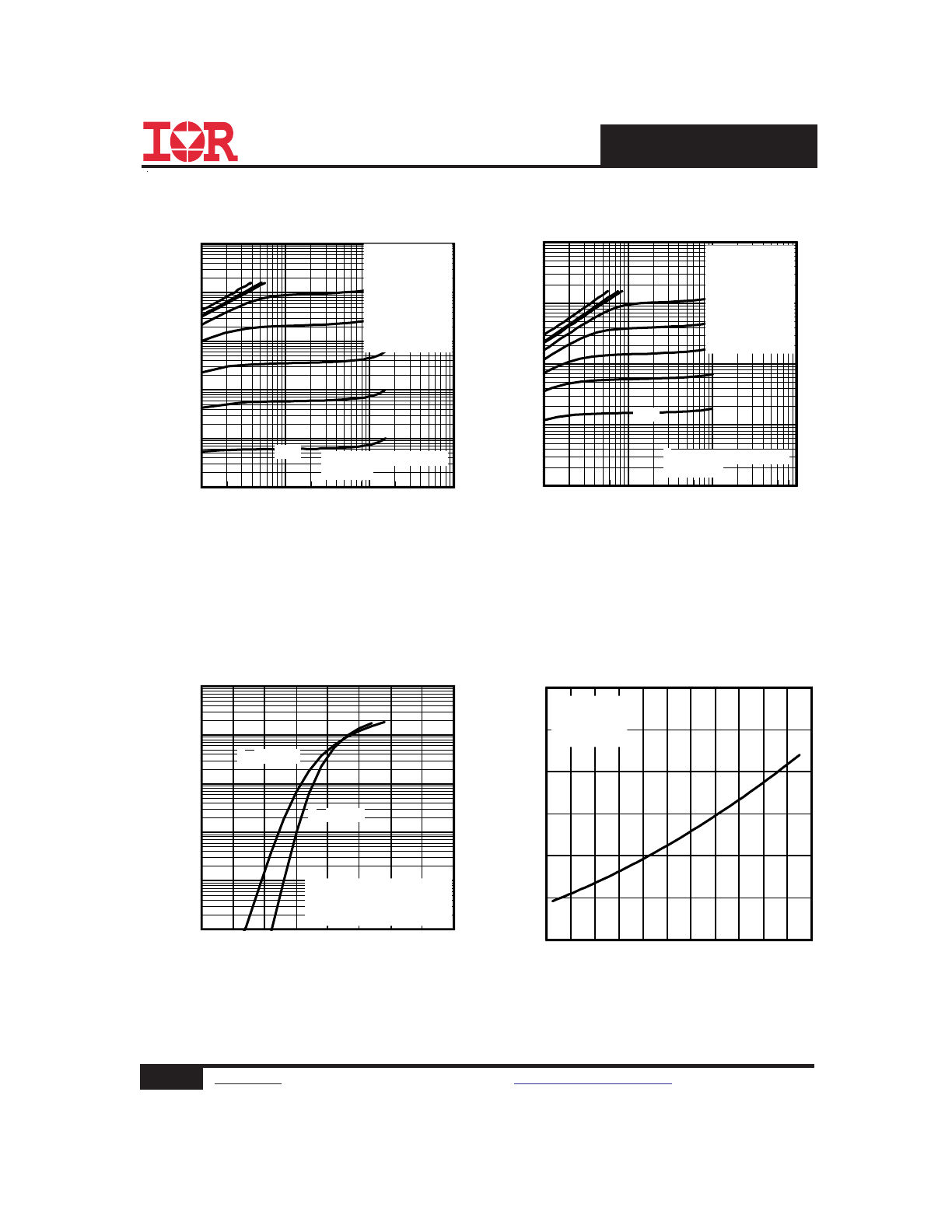
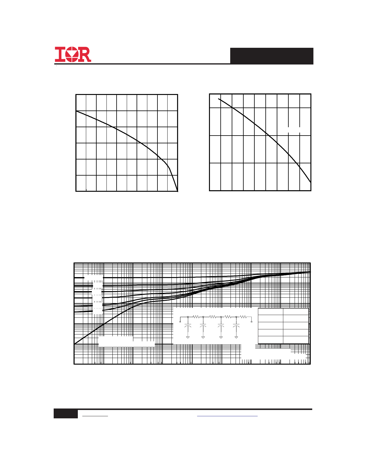
Fig 4. Normalized On-Resistance
Vs. Temperature
Fig 2. Typical Output Characteristics
Fig 1. Typical Output Characteristics
Fig 3. Typical Transfer Characteristics
0.1
1
10
100
VDS, Drain-to-Source Voltage (V)
0.01
0.1
1
10
100
1000
I D
, D
ra
in
-t
o-
S
ou
rc
e
C
ur
re
nt
(
A
)
≤ 60µs PULSE WIDTH
Tj = 25°C
2.3V
VGS
TOP
10V
5.0V
4.5V
3.5V
3.0V
2.7V
2.5V
BOTTOM
2.3V
0.1
1
10
100
VDS, Drain-to-Source Voltage (V)
0.1
1
10
100
1000
I D
, D
ra
in
-t
o-
S
ou
rc
e
C
ur
re
nt
(
A
)
≤ 60µs PULSE WIDTH
Tj = 150°C
2.3V
VGS
TOP
10V
5.0V
4.5V
3.5V
3.0V
2.7V
2.5V
BOTTOM
2.3V
1.0
2.0
3.0
4.0
5.0
VGS, Gate-to-Source Voltage (V)
0.01
0.1
1
10
100
1000
I D
, D
ra
in
-t
o-
S
ou
rc
e
C
ur
re
nt
(
A
)
VDS = 15V
≤ 60µs PULSE WIDTH
TJ = 25°C
TJ = 150°C
-60 -40 -20
0
20 40 60 80 100 120 140 160
TJ , Junction Temperature (°C)
0.5
1.0
1.5
2.0
R
D
S
(o
n)
,
D
ra
in
-t
o-
S
ou
rc
e
O
n
R
es
is
ta
nc
e
(
N
or
m
al
iz
ed
)
ID = 25A
VGS = 10V
4
www.irf.com
©
2014 International Rectifier
Submit Datasheet Feedback
August 11, 2014
IRFH7932PbF
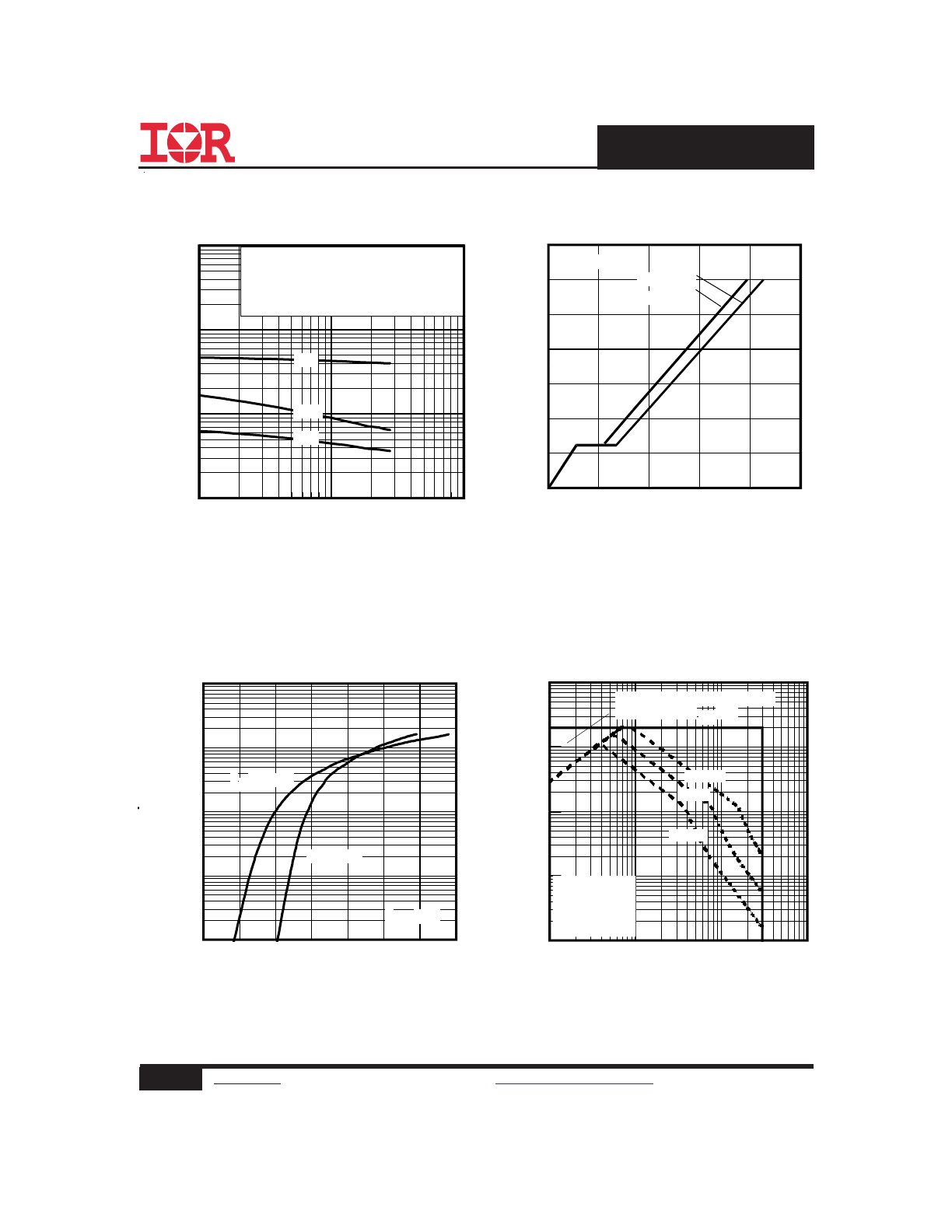
Fig 8. Maximum Safe Operating Area
Fig 6. Typical Gate Charge Vs.
Gate-to-Source Voltage
Fig 5. Typical Capacitance Vs.
Drain-to-Source Voltage
Fig 7. Typical Source-Drain Diode
Forward Voltage
1
10
100
VDS, Drain-to-Source Voltage (V)
100
1000
10000
100000
C
, C
ap
ac
ita
nc
e
(p
F
)
Coss
Crss
Ciss
VGS = 0V, f = 1 MHZ
Ciss = Cgs + Cgd, C ds SHORTED
Crss = Cgd
Coss = Cds + Cgd
0
20
40
60
80
100
QG Total Gate Charge (nC)
0
2
4
6
8
10
12
14
V
G
S
, G
at
e-
to
-S
ou
rc
e
V
ol
ta
ge
(
V
)
VDS= 24V
VDS= 15V
ID= 20A
0.2
0.4
0.6
0.8
1.0
1.2
1.4
1.6
VSD, Source-to-Drain Voltage (V)
0.1
1
10
100
1000
I S
D
, R
ev
er
se
D
ra
in
C
ur
re
nt
(
A
)
TJ = 25°C
TJ = 150°C
VGS = 0V
0
1
10
100
VDS, Drain-to-Source Voltage (V)
0.1
1
10
100
1000
I D
,
D
ra
in
-t
o-
S
ou
rc
e
C
ur
re
nt
(
A
)
OPERATION IN THIS AREA
LIMITED BY R DS(on)
TA = 25°C
Tj = 150°C
Single Pulse
100µsec
1msec
10msec
5
www.irf.com
©
2014 International Rectifier
Submit Datasheet Feedback
August 11, 2014
IRFH7932PbF
Fig 11. Maximum Effective Transient Thermal Impedance, Junction-to-Ambient
Fig 9. Maximum Drain Current Vs.
Ambient Temperature
Fig 10. Threshold Voltage Vs. Temperature
25
50
75
100
125
150
TJ , Ambient Temperature (°C)
0
5
10
15
20
25
30
I D
,
D
ra
in
C
ur
re
nt
(
A
)
-75
-50
-25
0
25
50
75
100 125 150
TJ , Temperature ( °C )
0.8
1.2
1.6
2.0
V
G
S
(t
h)
G
at
e
th
re
sh
ol
d
V
ol
ta
ge
(
V
)
ID = 100µA
1E-006
1E-005
0.0001
0.001
0.01
0.1
1
10
100
t1 , Rectangular Pulse Duration (sec)
0.001
0.01
0.1
1
10
100
T
he
rm
al
R
es
po
ns
e
(
Z
th
JA
)
0.20
0.10
D = 0.50
0.02
0.01
0.05
SINGLE PULSE
( THERMAL RESPONSE )
Notes:
1. Duty Factor D = t1/t2
2. Peak Tj = P dm x Zthja + Tc
Ri (°C/W)
τi (sec)
0.54874 0.000128
2.05644 0.023270
7.36536 1.0678
6.44303 38.4
τ
J
τ
J
τ
1
τ
1
τ
2
τ
2
τ
3
τ
3
R
1
R
1
R
2
R
2
R
3
R
3
Ci i
/Ri
Ci=
τi/Ri
τ
τ
C
τ
4
τ
4
R
4
R
4
6
www.irf.com
©
2014 International Rectifier
Submit Datasheet Feedback
August 11, 2014
IRFH7932PbF
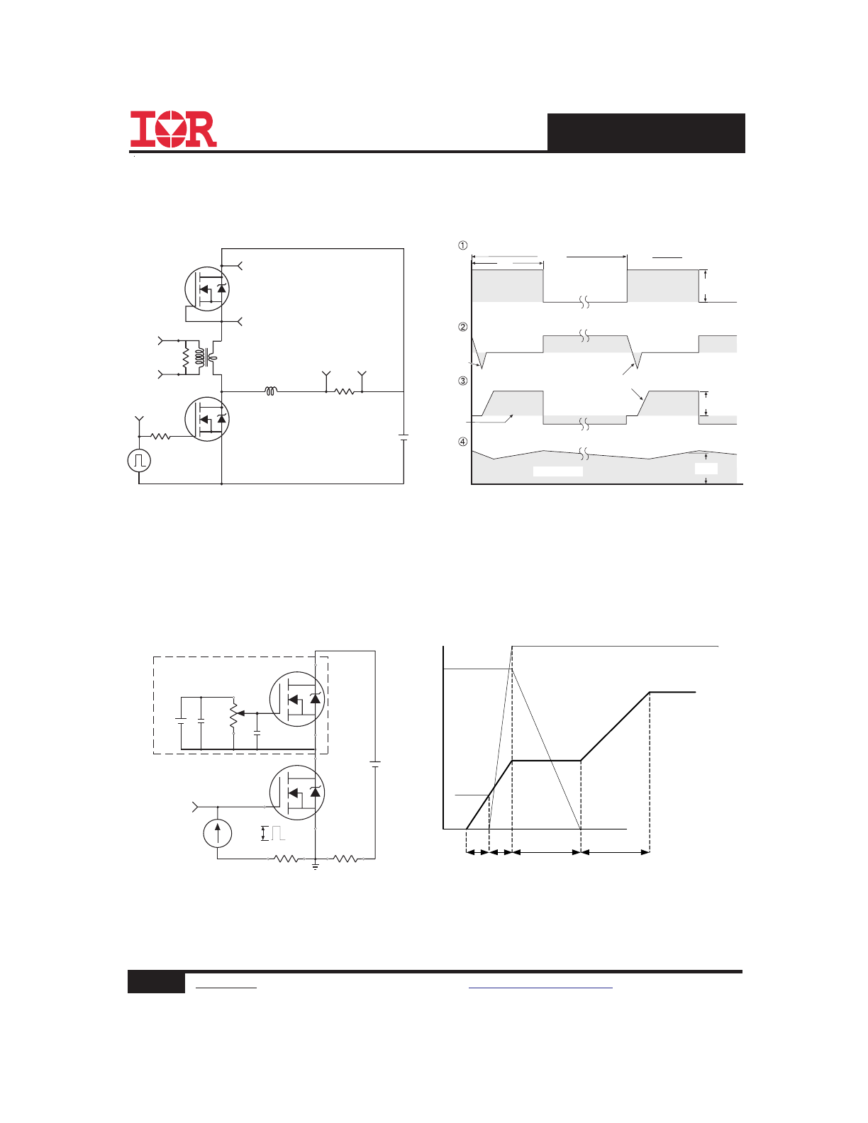
Fig 13. Maximum Avalanche Energy
vs. Drain Current
Fig 12. On-Resistance vs. Gate Voltage
Fig 14b. Unclamped Inductive Waveforms
Fig 14a. Unclamped Inductive Test Circuit
tp
V
(BR)DSS
I
AS
RG
IAS
0.01
Ω
tp
D.U.T
L
VDS
+
- VDD
DRIVER
A
15V
20V
Fig 15a. Switching Time Test Circuit
Fig 15b. Switching Time Waveforms
V
GS
V
DS
90%
10%
t
d(on)
t
d(off)
t
r
t
f
V
DS
Pulse Width ≤ 1 µs
Duty Factor ≤ 0.1
R
D
V
GS
R
G
D.U.T.
10V
+
-
V
DD
V
GS
2
3
4
5
6
7
8
9
10
VGS, Gate-to-Source Voltage (V)
0
2
4
6
8
10
12
14
16
R
D
S
(o
n)
,
D
ra
in
-t
o
-S
ou
rc
e
O
n
R
es
is
ta
nc
e
(m
Ω
)
TJ = 25°C
TJ = 125°C
ID = 25A
25
50
75
100
125
150
Starting TJ , Junction Temperature (°C)
0
10
20
30
40
50
60
70
E
A
S
,
S
in
gl
e
P
ul
se
A
va
la
nc
he
E
ne
rg
y
(m
J)
ID
TOP 5.86A
6.91A
BOTTOM 20.0A
7
www.irf.com
©
2014 International Rectifier
Submit Datasheet Feedback
August 11, 2014
IRFH7932PbF
D.U.T.
V
DS
I
D
I
G
3mA
V
GS
.3
µF
50K
Ω
.2
µF
12V
Current Regulator
Same Type as D.U.T.
Current Sampling Resistors
+
-
Fig 17. Gate Charge Test Circuit
Fig 16.
Peak Diode Recovery dv/dt Test Circuit for N-Channel
HEXFET
®
Power MOSFETs
Circuit Layout Considerations
• Low Stray Inductance
• Ground Plane
• Low Leakage Inductance
Current Transformer
P.W.
Period
di/dt
Diode Recovery
dv/dt
Ripple
≤ 5%
Body Diode Forward Drop
Re-Applied
Voltage
Reverse
Recovery
Current
Body Diode Forward
Current
V
GS
=10V
V
DD
I
SD
Driver Gate Drive
D.U.T. I
SD
Waveform
D.U.T. V
DS
Waveform
Inductor Curent
D =
P.W.
Period
*
V
GS
= 5V for Logic Level Devices
*
+
-
+
+
+
-
-
-
R
G
V
DD
• dv/dt controlled by R
G
• Driver same type as D.U.T.
• I
SD
controlled by Duty Factor "D"
• D.U.T. - Device Under Test
D.U.T
Fig 18. Gate Charge Waveform
Vds
Vgs
Id
Vgs(th)
Qgs1 Qgs2
Qgd
Qgodr
8
www.irf.com
©
2014 International Rectifier
Submit Datasheet Feedback
August 11, 2014
IRFH7932PbF
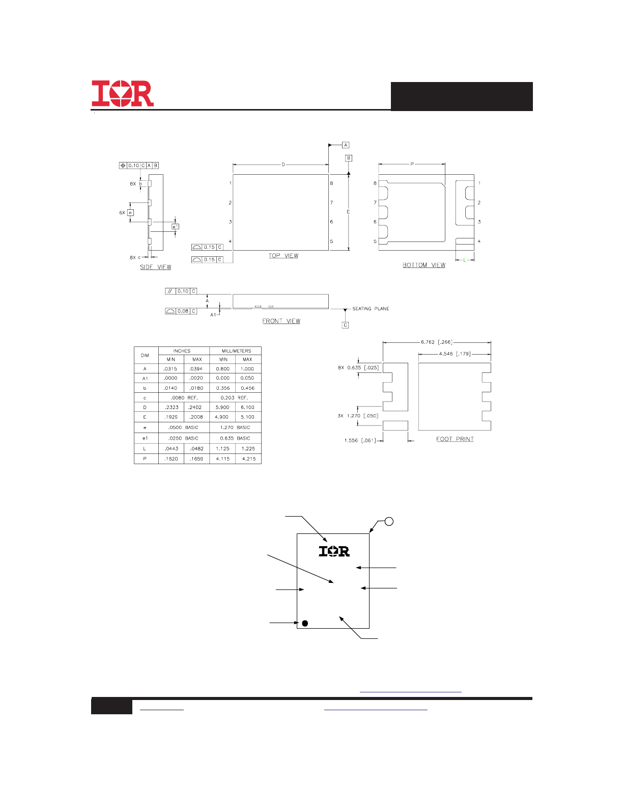
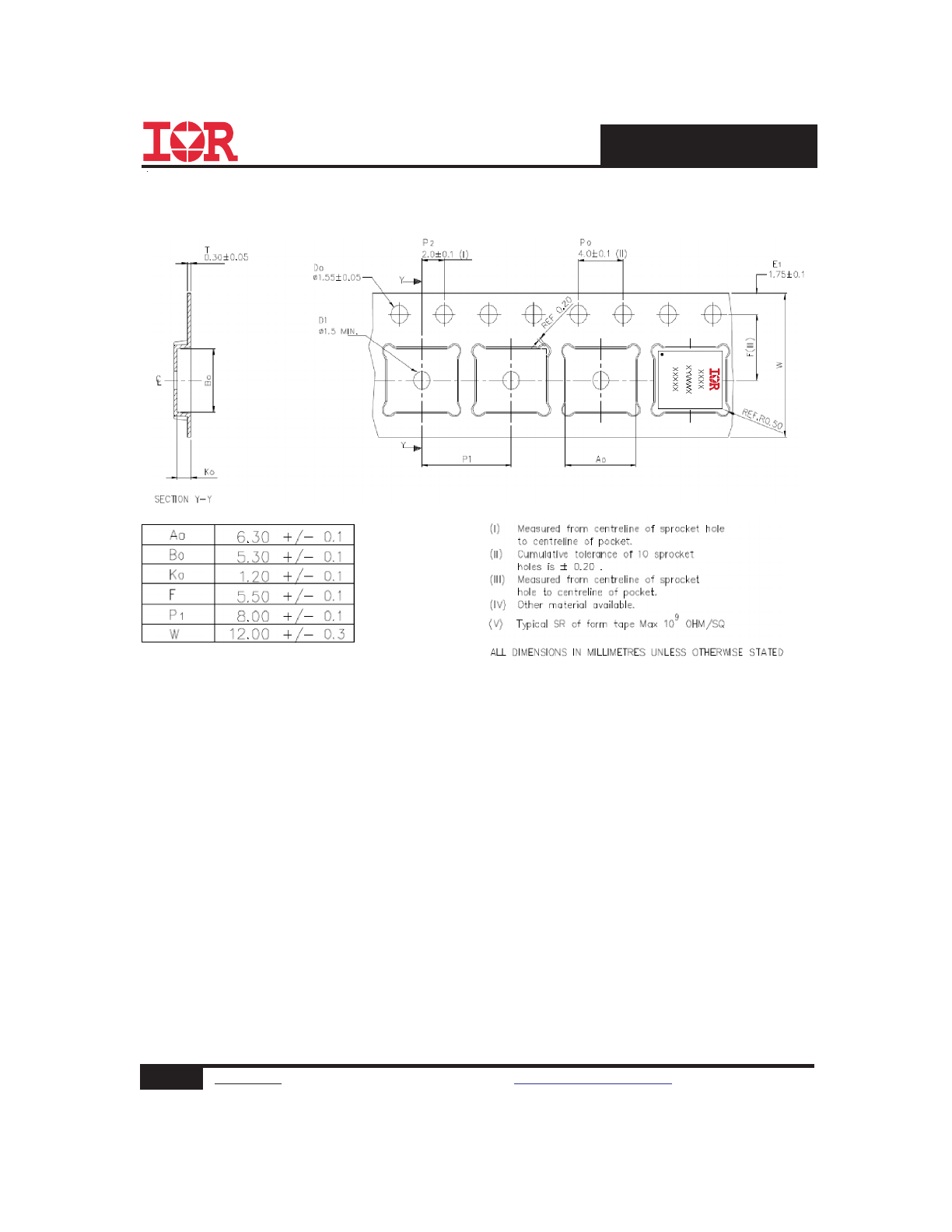
PQFN Part Marking
PQFN Package Details
MARKING CODE
(Per Marking Spec.)
XXXX
XYWWX
XXXXX
INTERNATIONAL
RECTIFIER LOGO
PART NUMBER
DATE CODE
ASSEMBLY SITE CODE
(Per SCOP 200-002)
PIN 1
IDENTIFIER
LOT CODE
(Eng Mode - Min. last 4 digits of EATI #)
(Prod Mode - 4 digits SPN code)
TOP MARKING (LASER)
6
Note: For the most current drawing please refer to IR website at:
http://www.irf.com/package/
9
www.irf.com
©
2014 International Rectifier
Submit Datasheet Feedback
August 11, 2014
IRFH7932PbF
PQFN Tape and Reel
10
www.irf.com
©
2014 International Rectifier
Submit Datasheet Feedback
August 11, 2014
IRFH7932PbF
IR WORLD HEADQUARTERS: 101 N. Sepulveda Blvd., El Segundo, California 90245, USA
To contact International Rectifier, please visit
http://www.irf.com/whoto-call/
Date
Comments
• Updated ordering information to reflect the End-Of-life (EOL) of the mini-reel option (EOL notice #259)
• Updated data sheet with new IR corporate template
8/1/2014
• Updated data sheet with PQFN Tape and Reel Diagram from Datasheet IRFH7934PbF
Revision History
12/16/2013
Notes:
Repetitive rating; pulse width limited by max. junction temperature.
Starting T
J
= 25°C, L = 0.078mH, R
G
= 25
Ω, I
AS
= 20A.
Pulse width ≤ 400µs; duty cycle ≤ 2%.
Rthjc is guaranteed by design
When mounted on 1 inch square 2 oz copper pad on 1.5x1.5 in. board of FR-4 material.
MSL
1
(per JEDEC J-STD-020D
†††
)
RoHS Compliant
Moisture Sensitivity Level
SO-8
Yes
Qualification Information
†
Qualification level
Consumer
††
(per JEDEC JESD47F
†††
guidelines)
Qualification standards can be found at International Rectifier’s web site
http://www.irf.com/product-info/reliability
Higher qualification ratings may be available should the user have such requirements.
Please contact your International Rectifier sales representative for further information:
http://www.irf.com/whoto-call/salesrep/
Applicable version of JEDEC standard at the time of product release.