
HEXFET
®
Power MOSFET
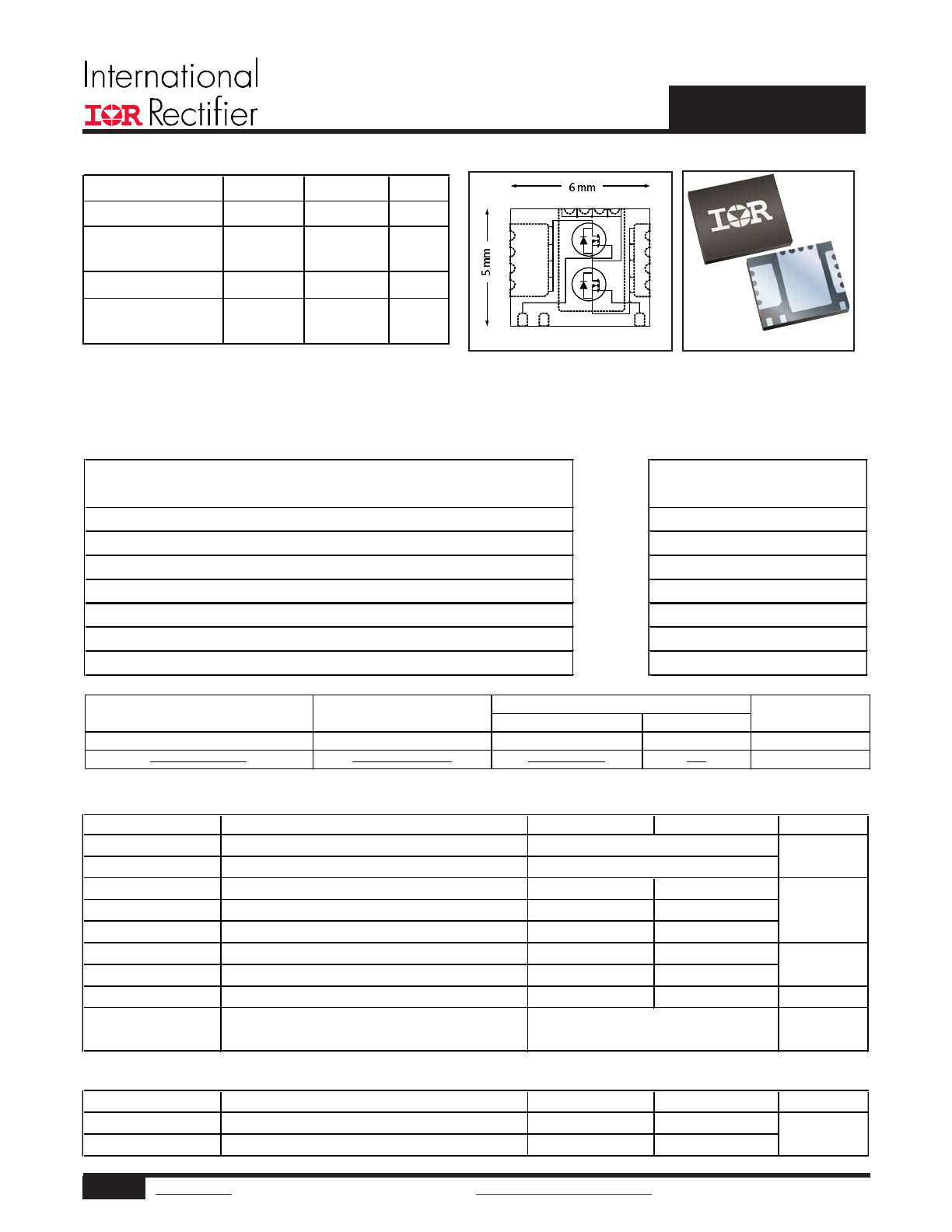
Dual PQFN 5X6 mm
Absolute Maximum Ratings
Parameter
Q1 Max.
Q2 Max.
Units
V
DS
Drain-to-Source Voltage
V
V
GS
Gate-to-Source Voltage
I
D
@ T
A
= 25°C
Continuous Drain Current, V
GS
@ 10V
13
28
I
D
@ T
A
= 70°C
Continuous Drain Current, V
GS
@ 10V
10
23
A
I
DM
Pulsed Drain Current
c
100
230
P
D
@T
A
= 25°C
Power Dissipation
2.4
3.4
W
P
D
@T
A
= 70°C
Power Dissipation
1.5
2.2
Linear Derating Factor
g
0.019
0.027
W/°C
T
J
Operating Junction and
°C
T
STG
Storage Temperature Range
Thermal Resistance
Parameter
Q1 Max.
Q2 Max.
Units
R
θJC
Junction-to-Case
f
7.7
2.5
°C/W
R
θJA
Junction-to-Ambient
g
53
37
± 20
30
-55 to + 150
Applications
•
Control and synchronous MOSFET for buck converters
Features and Benefits
Features
Benefits
Q1
Q2
V
DS
30
30
V
R
DS(on) max
(@V
GS
= 10V)
8.6
3.0
m
:
Q
g (typical)
8.3
34
nC
I
D
(@T
A
= 25°C)
13
28
A
Increased power density
(50% vs two PQFN 5x6)
Low charge control MOSFET (8.3 nC typical)
Lower switching losses
Low R
DSon
synchronous MOSFET (< 3.0 m
Ω)
results in Lower conduction losses
100% Rg tested
⇒
Increased reliability
Low Profile (
≤ 0.9 mm)
Increased power density
Compatible with Existing Surface Mount Techniques
Easier manufacturing
RoHS Compliant Containing no Lead, no Bromide and no Halogen
Environmentally Friendlier
MSL2, Consumer Qualification
Increased reliability
Control and synchronous FET in one package
*
1&
'
6
*
6'
IRFH7911PbF
Form
Quantity
IRFH7911TRPbF
PQFN 5mm x 6mm
Tape and Reel
4000
IRFH7911TR2PbF
PQFN 5mm x 6mm
Tape and Reel
400
EOL notice # 259
Orderable part number
Package Type
Standard Pack
Note
1
www.irf.com
©
2014 International Rectifier
Submit Datasheet Feedback
May 9, 2014
2
www.irf.com
©
2014 International Rectifier
Submit Datasheet Feedback
May 9, 2014
IRFH7911PbF
Static @ T
J
= 25°C (unless otherwise specified)
Parameter
Min.
Typ.
Max.
Units
BV
DSS
Drain-to-Source Breakdown Voltage
Q1&Q2
30
–––
–––
V
ΔΒV
DSS
/
ΔT
J
Breakdown Voltage Temp. Coefficient
Q1
–––
0.021
–––
V/°C
Q2
–––
0.022
–––
Q1
–––
7.2
8.6
R
DS(on)
Static Drain-to-Source On-Resistance
–––
11.1
14.5
m
Ω
Q2
–––
2.4
3.0
–––
3.4
4.0
V
GS(th)
Gate Threshold Voltage
Q1&Q2
1.35
–––
2.35
V
ΔV
GS(th)
/
ΔT
J
Gate Threshold Voltage Coefficient
Q1
–––
-6.8
–––
mV/°C
Q2
–––
-6.4
–––
I
DSS
Drain-to-Source Leakage Current
Q1&Q2
–––
–––
1.0
μA
Q1&Q2
–––
–––
150
I
GSS
Gate-to-Source Forward Leakage
Q1&Q2
–––
–––
100
nA
Gate-to-Source Reverse Leakage
Q1&Q2
–––
–––
-100
gfs
Forward Transconductance
Q1
17
–––
–––
S
Q2
106
–––
–––
Q
g
Total Gate Charge
Q1
–––
8.3
12
Q2
–––
34
51
Q
gs1
Pre-Vth Gate-to-Source Charge
Q1
–––
2.0
–––
Q1
Q2
–––
7.9
–––
V
DS
= 15V
Q
gs2
Post-Vth Gate-to-Source Charge
Q1
–––
1.0
–––
nC
V
GS
= 4.5V, I
D
= 10A
Q2
–––
3.6
–––
Q
gd
Gate-to-Drain Charge
Q1
–––
3.2
–––
Q2
Q2
–––
11
–––
V
DS
= 15V
Q
godr
Gate Charge Overdrive
Q1
–––
2.1
–––
V
GS
= 4.5V, I
D
= 21A
Q2
–––
12
–––
Q
sw
Switch Charge (Q
gs2
+ Q
gd
)
Q1
–––
4.2
–––
Q2
–––
15
–––
Q
oss
Output Charge
Q1
–––
5.0
–––
nC
Q2
–––
19
–––
R
G
Gate Resistance
Q1
–––
1.8
–––
Ω
Q2
–––
0.7
–––
t
d(on)
Turn-On Delay Time
Q1
–––
12
–––
Q2
–––
22
–––
t
r
Rise Time
Q1
–––
15
–––
I
D
= 10A
Q2
–––
35
–––
ns
t
d(off)
Turn-Off Delay Time
Q1
–––
12
–––
Q2
–––
28
–––
t
f
Fall Time
Q1
–––
5.9
–––
I
D
= 21A
Q2
–––
14
–––
C
iss
Input Capacitance
Q1
–––
1060
–––
Q2
–––
4450
–––
C
oss
Output Capacitance
Q1
–––
230
–––
pF
Q2
–––
850
–––
C
rss
Reverse Transfer Capacitance
Q1
–––
110
–––
Q2
–––
440
–––
Avalanche Characteristics
Parameter
Q1 Max.
Q2 Max.
Units
E
AS
Single Pulse Avalanche Energy
d
12
32
mJ
I
AR
Avalanche Current
c
10
21
A
Diode Characteristics
Parameter
Min.
Typ.
Max.
Units
I
S
Continuous Source Current
Q1
–––
–––
3.0
A
(Body Diode)
Q2
–––
–––
3.0
I
SM
Pulsed Source Current
Q1
–––
–––
100
A
(Body Diode)
c
Q2
–––
–––
230
V
SD
Diode Forward Voltage
Q1
–––
–––
1.0
V
Q2
–––
–––
1.0
t
rr
Reverse Recovery Time
Q1
–––
13
20
ns
Q2
–––
20
29
Q
rr
Reverse Recovery Charge
Q1
–––
13
20
nC
Q2
–––
24
36
V
GS
= 4.5V, I
D
= 10A
e
V
GS
= 4.5V, I
D
= 21A
e
V
DS
= 15V, I
D
= 21A
V
DD
= 15V, V
GS
= 4.5V
V
GS
= 10V, I
D
= 26A
e
Q1: V
DS
= V
GS
, I
D
= 25μA
V
DS
= 15V, I
D
= 10A
V
DS
= 24V, V
GS
= 0V, T
J
= 125°C
Conditions
V
GS
= 0V, I
D
= 250μA
Reference to 25°C, I
D
= 1mA
V
GS
= 10V, I
D
= 12A
e
MOSFET symbol
Q2: V
DS
= V
GS
, I
D
= 100μA
V
DS
= 16V, V
GS
= 0V
Q1
V
GS
= 20V
V
GS
= -20V
V
DS
= 24V, V
GS
= 0V
Conditions
Q2
–––
Q1 T
J
= 25°C, I
F
= 10A,
V
DD
= 15V, di/dt = 280A/μs
e
T
J
= 25°C, I
S
= 10A, V
GS
= 0V
e
showing the
integral reverse
p-n junction diode.
T
J
= 25°C, I
S
= 21A, V
GS
= 0V
e
Q2 T
J
= 25°C, I
F
= 21A,
V
DD
= 15V, di/dt = 300A/μs
e
V
DD
= 15V, V
GS
= 4.5V
R
G
=1.8
Ω
–––
V
DS
= 15V
R
G
=1.8
Ω
V
GS
= 0V
ƒ = 1.0MHz
Typ.
3
www.irf.com
©
2014 International Rectifier
Submit Datasheet Feedback
May 9, 2014
IRFH7911PbF
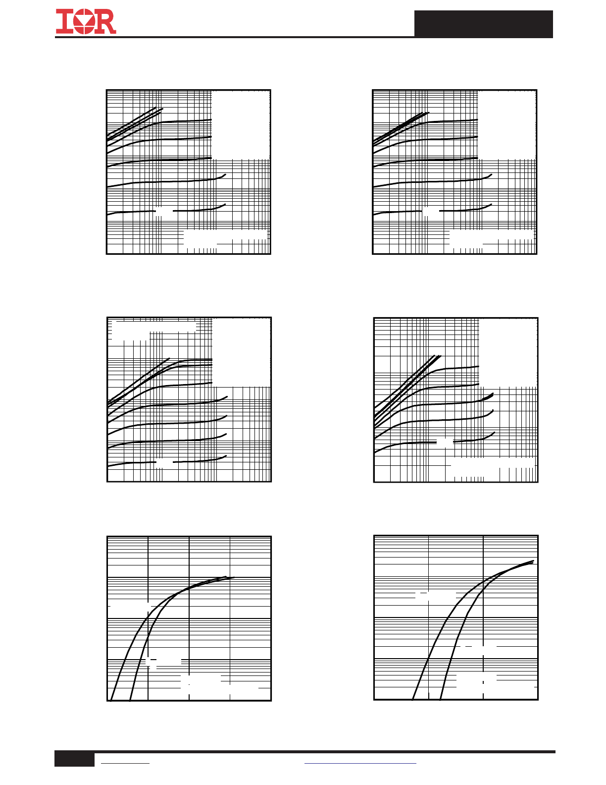
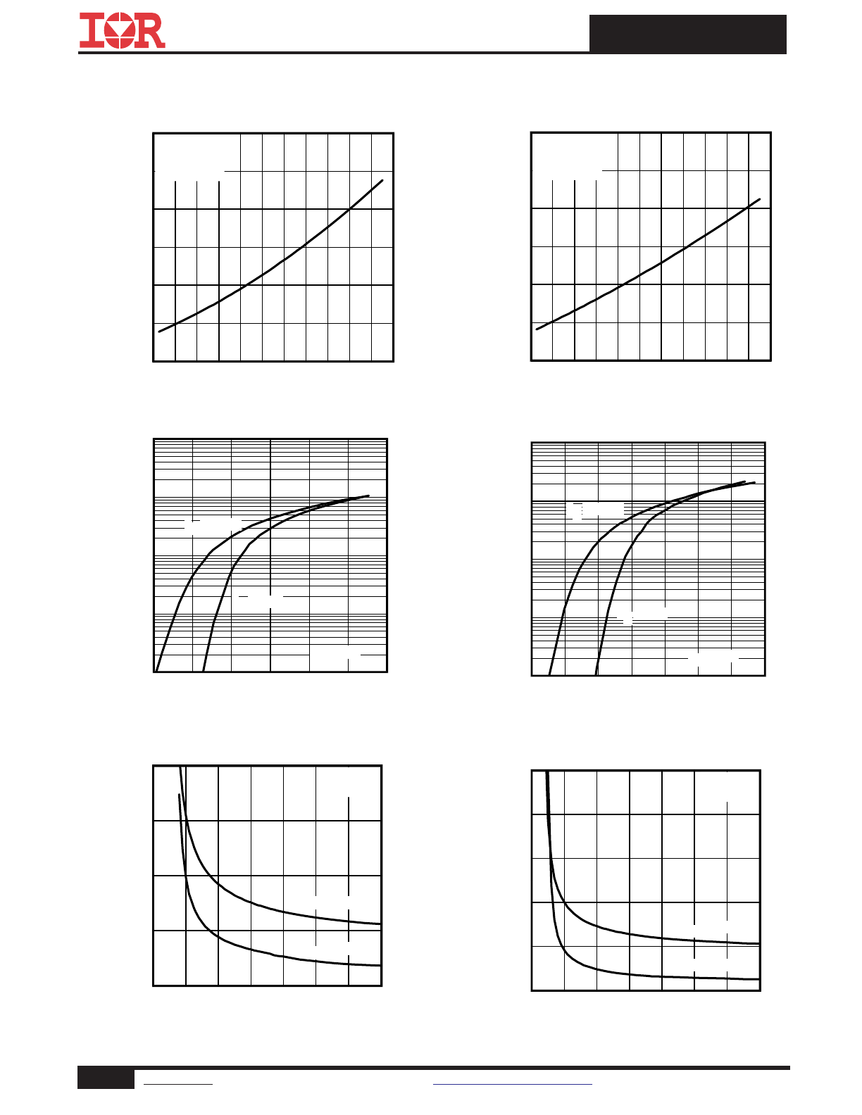
Fig 2. Typical Output Characteristics
Fig 1. Typical Output Characteristics
Q1 - Control FET
Q2 - Synchronous FET
Typical Characteristics
Fig 3. Typical Output Characteristics
Fig 4. Typical Output Characteristics
Fig 5. Typical Transfer Characteristics
Fig 6. Typical Transfer Characteristics
0.1
1
10
100
VDS, Drain-to-Source Voltage (V)
0.1
1
10
100
1000
I D
, D
ra
in
-t
o-
S
ou
rc
e
C
ur
re
nt
(
A
)
VGS
TOP
10V
5.0V
4.5V
3.5V
3.0V
2.7V
2.5V
BOTTOM
2.3V
≤60μs PULSE WIDTH
Tj = 150°C
2.3V
2
3
4
5
6
VGS, Gate-to-Source Voltage (V)
0.1
1
10
100
1000
I D
, D
ra
in
-t
o-
S
ou
rc
e
C
ur
re
nt
(A
)
TJ = 25°C
TJ = 150°C
VDS = 15V
≤60μs PULSE WIDTH
0.1
1
10
100
VDS, Drain-to-Source Voltage (V)
0.01
0.1
1
10
100
1000
I D
, D
ra
in
-t
o-
S
ou
rc
e
C
ur
re
nt
(
A
)
VGS
TOP
10V
5.0V
4.5V
3.5V
3.0V
2.7V
2.5V
BOTTOM
2.3V
≤60μs PULSE WIDTH
Tj = 25°C
2.3V
0.1
1
10
100
VDS, Drain-to-Source Voltage (V)
1
10
100
1000
I D
, D
ra
in
-t
o-
S
ou
rc
e
C
ur
re
nt
(
A
)
VGS
TOP
10V
5.0V
4.5V
3.5V
3.0V
2.7V
2.5V
BOTTOM
2.3V
≤60μs PULSE WIDTH
Tj = 150°C
2.3V
1
2
3
4
VGS, Gate-to-Source Voltage (V)
0.1
1
10
100
1000
I D
, D
ra
in
-t
o-
S
ou
rc
e
C
ur
re
nt
(A
)
TJ = 25°C
TJ = 150°C
VDS = 15V
≤60μs PULSE WIDTH
0.1
1
10
100
VDS, Drain-to-Source Voltage (V)
0.01
0.1
1
10
100
1000
I D
, D
ra
in
-t
o-
S
ou
rc
e
C
ur
re
nt
(
A
)
VGS
TOP
10V
5.0V
4.5V
3.5V
3.0V
2.7V
2.5V
BOTTOM
2.3V
≤60μs PULSE WIDTH
Tj = 25°C
2.3V
4
www.irf.com
©
2014 International Rectifier
Submit Datasheet Feedback
May 9, 2014
IRFH7911PbF
Q1 - Control FET
Q2 - Synchronous FET
Typical Characteristics
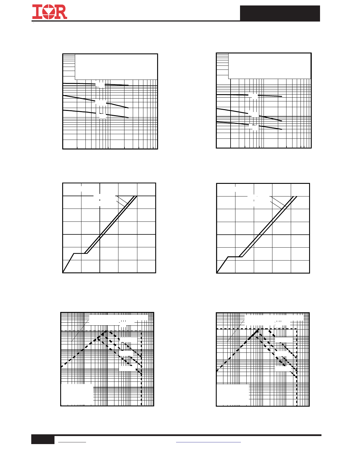
Fig 7. Typical Capacitance vs. Drain-to-Source Voltage Fig 8. Typical Capacitance vs. Drain-to-Source Voltage
Fig 9. Typical Gate Charge vs. Gate-to-Source Voltage
Fig 10. Typical Gate Charge vs. Gate-to-Source
Voltage
Fig 11. Maximum Safe Operating Area
Fig 12. Maximum Safe Operating Area
1
10
100
VDS, Drain-to-Source Voltage (V)
10
100
1000
10000
C
, C
ap
ac
ita
nc
e
(p
F
)
VGS = 0V, f = 1 MHZ
Ciss = Cgs + Cgd, Cds SHORTED
Crss = Cgd
Coss = Cds + Cgd
Coss
Crss
Ciss
0
5
10
15
20
25
Qg, Total Gate Charge (nC)
0
2
4
6
8
10
12
14
V
G
S
, G
at
e-
to
-S
ou
rc
e
V
ol
ta
ge
(
V
)
VDS= 24V
VDS= 15V
ID= 10A
0.01
0.1
1
10
100
VDS , Drain-to-Source Voltage (V)
0.01
0.1
1
10
100
1000
I D
,
D
ra
in
-t
o-
S
ou
rc
e
C
ur
re
nt
(
A
)
Tc = 25°C
Tj = 150°C
Single Pulse
1msec
10msec
OPERATION IN THIS AREA
LIMITED BY R DS(on)
100μsec
1
10
100
VDS, Drain-to-Source Voltage (V)
100
1000
10000
100000
C
, C
ap
ac
ita
nc
e
(p
F
)
VGS = 0V, f = 1 MHZ
Ciss = Cgs + Cgd, Cds SHORTED
Crss = Cgd
Coss = Cds + Cgd
Coss
Crss
Ciss
0
20
40
60
80
100
Qg, Total Gate Charge (nC)
0
2
4
6
8
10
12
14
V
G
S
, G
at
e-
to
-S
ou
rc
e
V
ol
ta
ge
(
V
)
VDS= 24V
VDS= 15V
ID= 21A
0.01
0.1
1
10
100
VDS , Drain-to-Source Voltage (V)
0.1
1
10
100
1000
I D
,
D
ra
in
-t
o-
S
ou
rc
e
C
ur
re
nt
(
A
)
Tc = 25°C
Tj = 150°C
Single Pulse
1msec
10msec
OPERATION IN THIS AREA
LIMITED BY R DS(on)
100μsec
5
www.irf.com
©
2014 International Rectifier
Submit Datasheet Feedback
May 9, 2014
IRFH7911PbF
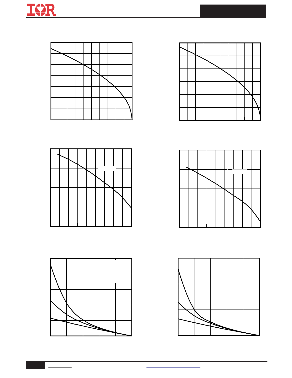
Fig 17. Typical On-Resistance vs.Gate Voltage
Q1 - Control FET
Q2 - Synchronous FET
Typical Characteristics
Fig 13. Normalized On-Resistance vs. Temperature
Fig 14. Normalized On-Resistance vs. Temperature
Fig 15. Typical Source-Drain Diode Forward Voltage
Fig 16. Typical Source-Drain Diode Forward Voltage
Fig 18. Typical On-Resistance vs.Gate Voltage
0.4
0.6
0.8
1.0
1.2
1.4
1.6
VSD, Source-to-Drain Voltage (V)
0.10
1.00
10
100
1000
I S
D
, R
ev
er
se
D
ra
in
C
ur
re
nt
(
A
)
TJ = 25°C
TJ = 150°C
VGS = 0V
2
4
6
8
10
12
14
16
VGS, Gate-to-Source Voltage (V)
5
10
15
20
25
R
D
S
(o
n)
,
D
ra
in
-t
o
-S
ou
rc
e
O
n
R
es
is
ta
nc
e
(m
Ω
)
TJ = 25°C
TJ = 125°C
ID = 13A
0.2
0.4
0.6
0.8
1.0
1.2
1.4
1.6
VSD, Source-to-Drain Voltage (V)
0.10
1.00
10
100
1000
I S
D
, R
ev
er
se
D
ra
in
C
ur
re
nt
(
A
)
TJ = 25°C
TJ = 150°C
VGS = 0V
2
4
6
8
10
12
14
16
VGS, Gate-to-Source Voltage (V)
2
4
6
8
10
12
R
D
S
(o
n)
,
D
ra
in
-t
o
-S
ou
rc
e
O
n
R
es
is
ta
nc
e
(m
Ω
)
TJ = 25°C
TJ = 125°C
ID = 26A
-60 -40 -20
0
20 40 60 80 100 120 140 160
TJ , Junction Temperature (°C)
0.5
1.0
1.5
2.0
R
D
S
(o
n)
,
D
ra
in
-t
o-
S
ou
rc
e
O
n
R
es
is
ta
nc
e
(
N
or
m
al
iz
ed
)
ID = 26A
VGS = 10V
-60 -40 -20
0
20 40 60 80 100 120 140 160
TJ , Junction Temperature (°C)
0.5
1.0
1.5
2.0
R
D
S
(o
n)
,
D
ra
in
-t
o-
S
ou
rc
e
O
n
R
es
is
ta
nc
e
(
N
or
m
al
iz
ed
)
ID = 12A
VGS = 10V
6
www.irf.com
©
2014 International Rectifier
Submit Datasheet Feedback
May 9, 2014
IRFH7911PbF
Q1 - Control FET
Q2 - Synchronous FET
Typical Characteristics
Fig 19. Maximum Drain Current vs. Ambient Temp.
Fig 20. Maximum Drain Current vs. Ambient Temp.
Fig 21. Threshold Voltage vs. Temperature
Fig 22. Threshold Voltage vs. Temperature
Fig 23. Maximum Avalanche Energy vs. Drain Current
Fig 24. Maximum Avalanche Energy vs. Drain Current
-75
-50
-25
0
25
50
75
100 125 150
TJ , Temperature ( °C )
0.5
1.0
1.5
2.0
2.5
V
G
S
(t
h)
G
at
e
th
re
sh
ol
d
V
ol
ta
ge
(
V
)
ID = 25μA
25
50
75
100
125
150
Starting TJ, Junction Temperature (°C)
0
10
20
30
40
50
E
A
S
,
S
in
gl
e
P
ul
se
A
va
la
nc
he
E
ne
rg
y
(m
J)
I D
TOP
2.3A
3.1A
BOTTOM
10A
-75
-50
-25
0
25
50
75
100 125 150
TJ , Temperature ( °C )
0.5
1.0
1.5
2.0
2.5
V
G
S
(t
h)
G
at
e
th
re
sh
ol
d
V
ol
ta
ge
(
V
)
ID = 250μA
25
50
75
100
125
150
Starting TJ, Junction Temperature (°C)
0
50
100
150
E
A
S
,
S
in
gl
e
P
ul
se
A
va
la
nc
he
E
ne
rg
y
(m
J)
I D
TOP
5.4A
6.6A
BOTTOM
21A
25
50
75
100
125
150
TA , Ambient Temperature (°C)
0
2
4
6
8
10
12
14
I D
, D
ra
in
C
ur
re
nt
(
A
)
25
50
75
100
125
150
TA , Ambient Temperature (°C)
0
5
10
15
20
25
30
I D
, D
ra
in
C
ur
re
nt
(
A
)
7
www.irf.com
©
2014 International Rectifier
Submit Datasheet Feedback
May 9, 2014
IRFH7911PbF
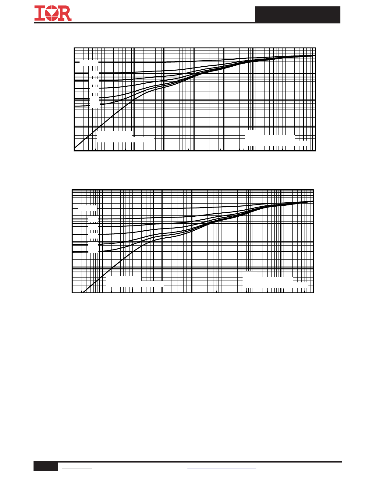
Fig 25. Maximum Effective Transient Thermal Impedance, Junction-to-Ambient (Q1)
Fig 26. Maximum Effective Transient Thermal Impedance, Junction-to-Ambient (Q2)
1E-006
1E-005
0.0001
0.001
0.01
0.1
1
10
100
t1 , Rectangular Pulse Duration (sec)
0.01
0.1
1
10
100
T
he
rm
al
R
es
po
ns
e
(
Z
th
JA
)
0.20
0.10
D = 0.50
0.02
0.01
0.05
SINGLE PULSE
( THERMAL RESPONSE )
Notes:
1. Duty Factor D = t1/t2
2. Peak Tj = P dm x Zthja + Tc
1E-006
1E-005
0.0001
0.001
0.01
0.1
1
10
100
t1 , Rectangular Pulse Duration (sec)
0.01
0.1
1
10
100
T
he
rm
al
R
es
po
ns
e
(
Z
th
JA
)
0.20
0.10
D = 0.50
0.02
0.01
0.05
SINGLE PULSE
( THERMAL RESPONSE )
Notes:
1. Duty Factor D = t1/t2
2. Peak Tj = P dm x Zthja + Tc
8
www.irf.com
©
2014 International Rectifier
Submit Datasheet Feedback
May 9, 2014
IRFH7911PbF
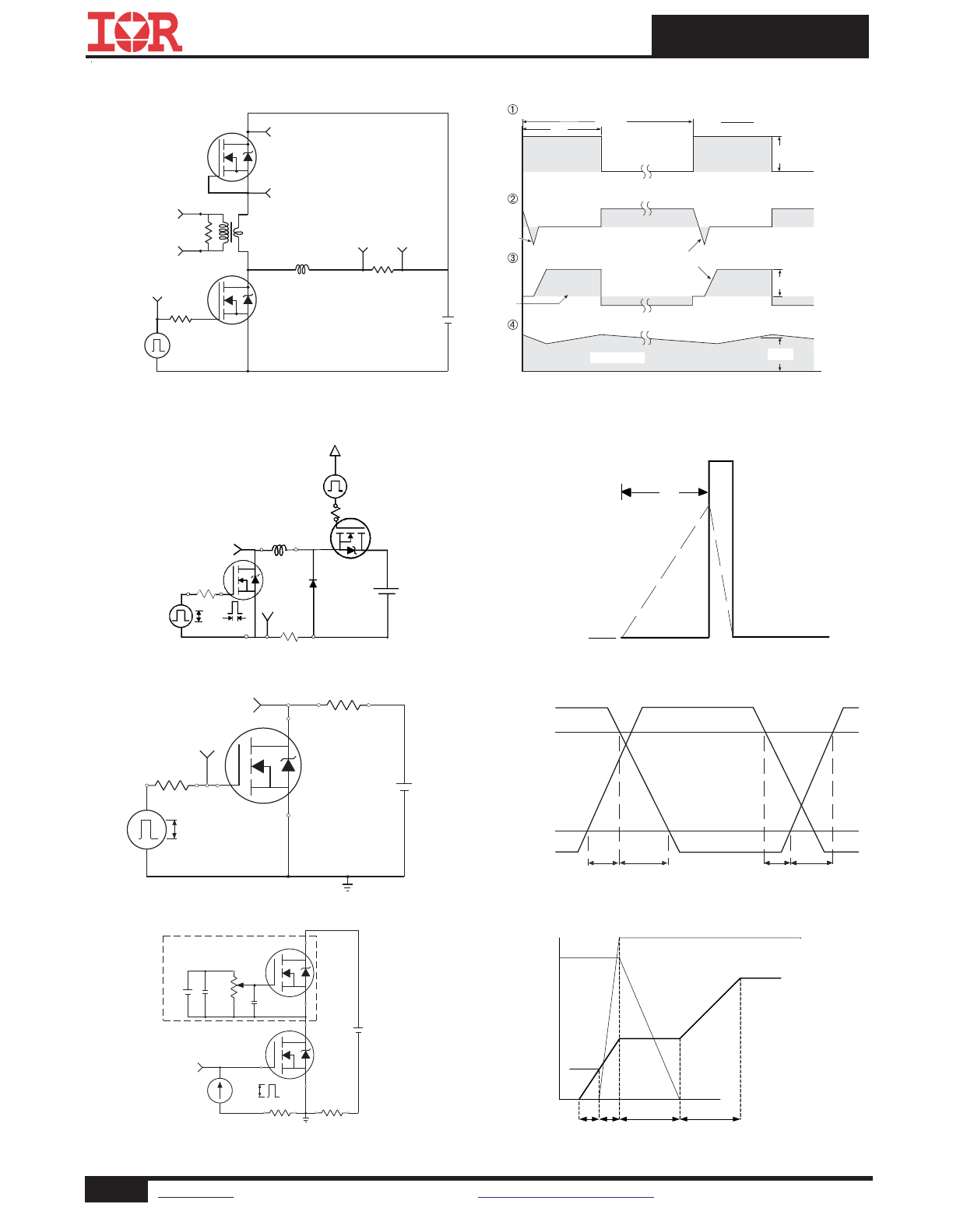
Fig 30a. Switching Time Test Circuit
Fig 30b. Switching Time Waveforms
Fig 29b. Unclamped Inductive Waveforms
Fig 29a. Unclamped Inductive Test Circuit
tp
V
(BR)DSS
I
AS
RG
IAS
0.01
Ω
tp
D.U.T
L
VDS
+
- VDD
DRIVER
A
15V
20V
V
GS
Fig 31a. Gate Charge Test Circuit
Fig 31b. Gate Charge Waveform
Vds
Vgs
Id
Vgs(th)
Qgs1 Qgs2
Qgd
Qgodr
Fig 28.
Peak Diode Recovery dv/dt Test Circuit for N-Channel HEXFET
®
Power MOSFETs
Circuit Layout Considerations
• Low Stray Inductance
• Ground Plane
• Low Leakage Inductance
Current Transformer
P.W.
Period
di/dt
Diode Recovery
dv/dt
Ripple
≤ 5%
Body Diode Forward Drop
Re-Applied
Voltage
Reverse
Recovery
Current
Body Diode Forward
Current
V
GS
=10V
V
DD
I
SD
Driver Gate Drive
D.U.T. I
SD
Waveform
D.U.T. V
DS
Waveform
Inductor Curent
D =
P.W.
Period
*
V
GS
= 5V for Logic Level Devices
*
+
-
+
+
+
-
-
-
R
G
V
DD
• dv/dt controlled by R
G
• Driver same type as D.U.T.
• I
SD
controlled by Duty Factor "D"
• D.U.T. - Device Under Test
D.U.T
Inductor Current
D.U.T.
V
DS
I
D
I
G
3mA
V
GS
.3
μF
50K
Ω
.2
μF
12V
Current Regulator
Same Type as D.U.T.
Current Sampling Resistors
+
-
V
DS
90%
10%
V
GS
t
d(on)
t
r
t
d(off)
t
f
V
DS
Pulse Width ≤ 1 µs
Duty Factor ≤ 0.1 %
R
D
V
GS
R
G
D.U.T.
10V
+
-
V
DD
V
GS
9
www.irf.com
©
2014 International Rectifier
Submit Datasheet Feedback
May 9, 2014
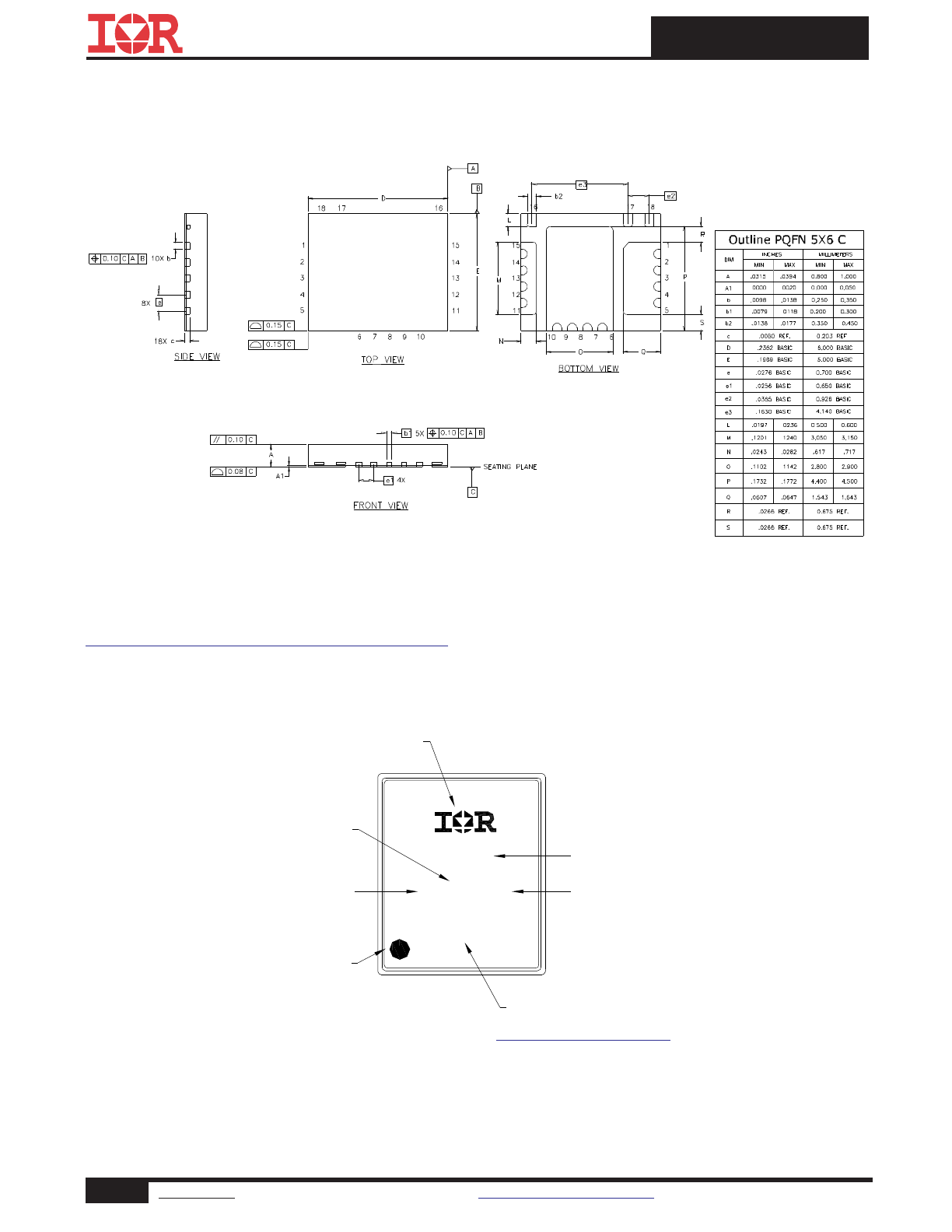
IRFH7911PbF
PQFN 5x6 Outline "C" Part Marking
PQFN 5x6 Outline "C" Package Details
Note: For the most current drawing please refer to IR website at:
http://www.irf.com/package/
XXXX
XYWWX
XXXXX
INTERNATIONAL
RECTIFIER LOGO
PART NUMBER
(“4 or 5 digits”)
MARKING CODE
(Per Marking Spec)
ASSEMBLY
SITE CODE
(Per SCOP 200-002)
DATE CODE
PIN 1
IDENTIFIER
LOT CODE
(Eng Mode - Min last 4 digits of EATI#)
(Prod Mode - 4 digits of SPN code)
For footprint and stencil design recommendations, please refer to application note AN-1136 at
http://www.irf.com/technical-info/appnotes/an-1136.pdf
10
www.irf.com
©
2014 International Rectifier
Submit Datasheet Feedback
May 9, 2014
IRFH7911PbF
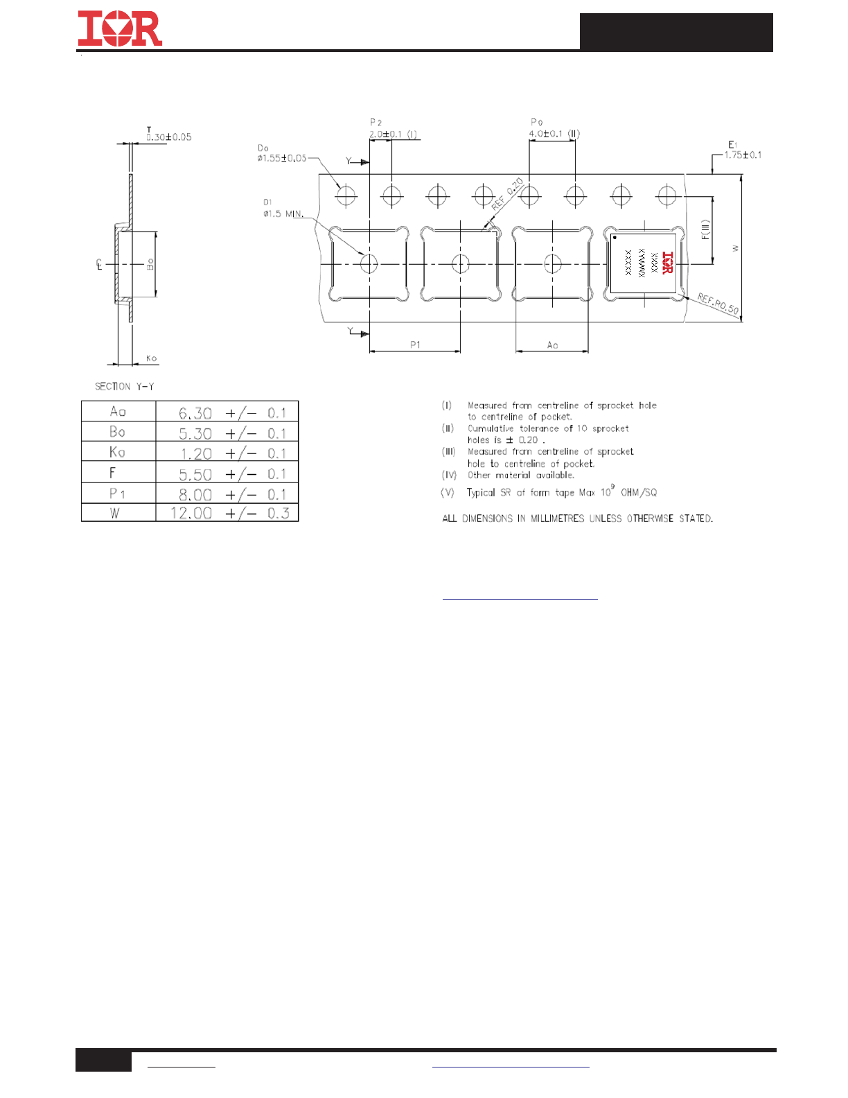
PQFN 5x6 Outline "C" Tape and Reel
Note: For the most current drawing please refer to IR website at:
http://www.irf.com/package/