
HEXFET
®
Power MOSFET
Notes
through
are on page 9
Features and Benefits
Applications
•
Secondary Side Synchronous Rectification
•
Inverters for DC Motors
•
DC-DC Brick Applications
•
Boost Converters
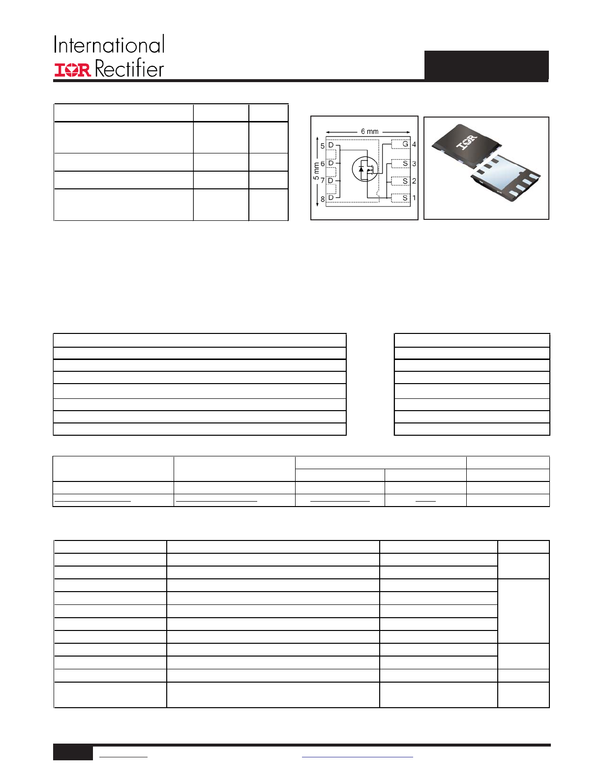
PQFN 5X6 mm
Absolute Maximum Ratings
Parameter
Units
V
DS
Drain-to-Source Voltage
V
GS
Gate-to-Source Voltage
I
D
@ T
A
= 25°C
Continuous Drain Current, V
GS
@ 10V
I
D
@ T
A
= 70°C
Continuous Drain Current, V
GS
@ 10V
I
D
@ T
C(Bottom)
= 25°C
Continuous Drain Current, V
GS
@ 10V
h
I
D
@ T
C(Bottom)
= 100°C
Continuous Drain Current, V
GS
@ 10V
I
DM
Pulsed Drain Current
c
P
D
@T
A
= 25°C
Power Dissipation g
P
D
@ T
C(Bottom)
= 25°C
Power Dissipation
g
Linear Derating Factor g
W/°C
T
J
Operating Junction and
T
STG
Storage Temperature Range
V
W
A
°C
Max.
24
86
400
±20
40
19
100
-55 to + 150
3.6
0.029
114
V
DS
40
V
R
DS(on) max
(@V
GS
= 10V)
3.5
m
Ω
Q
g (typical)
53
nC
R
G (typical)
1.4
Ω
I
D
(@T
c(Bottom)
= 25°C)
100h
A
Features
Benefits
Low R
DSon
(
≤ 3.5mΩ)
Lower Conduction Losses
Low Thermal Resistance to PCB (
≤ 1.1°C/W)
Enables better thermal dissipation
100% Rg tested
Increased Reliability
Low Profile (
≤ 0.9 mm)
results in Increased Power Density
Industry-Standard Pinout
⇒
Multi-Vendor Compatibility
Compatible with Existing Surface Mount Techniques
Easier Manufacturing
RoHS Compliant Containing no Lead, no Bromide and no Halogen
Environmentally Friendlier
MSL1, Industrial Qualification
Increased Reliability
IRFH5104PbF
1
www.irf.com
©
2015 International Rectifier
Submit Datasheet Feedback
March 16, 2015
Note
Form
Quantity
IRFH5104TRPBF
PQFN 5mm x 6mm
Tape and Reel
4000
IRFH5104TR2PBF
PQFN 5mm x 6mm
Tape and Reel
1000
EOL notice #259
Orderable part number
Package Type
Standard Pack
2
www.irf.com
©
2015 International Rectifier
Submit Datasheet Feedback
March 16, 2015
IRFH5104PbF
S
D
G
Thermal Resistance
Parameter
Typ.
Max.
Units
R
θJC
(Bottom)
Junction-to-Case f
–––
1.1
R
θJC
(Top)
Junction-to-Case
f
–––
15
°C/W
R
θJA
Junction-to-Ambient g
–––
35
R
θJA
(<10s)
Junction-to-Ambient
g
–––
22
Static @ T
J
= 25°C (unless otherwise specified)
Parameter
Min.
Typ.
Max. Units
BV
DSS
Drain-to-Source Breakdown Voltage
40
–––
–––
V
ΔΒV
DSS
/ΔT
J
Breakdown Voltage Temp. Coefficient
–––
0.05
–––
V/°C
R
DS(on)
Static Drain-to-Source On-Resistance
–––
2.9
3.5
V
GS(th)
Gate Threshold Voltage
2.0
–––
4.0
V
ΔV
GS(th)
Gate Threshold Voltage Coefficient
–––
-8.9
––– mV/°C
I
DSS
Drain-to-Source Leakage Current
–––
–––
20
–––
–––
250
I
GSS
Gate-to-Source Forward Leakage
–––
–––
100
Gate-to-Source Reverse Leakage
–––
–––
-100
gfs
Forward Transconductance
56
–––
–––
S
Q
g
Total Gate Charge
–––
53
80
Q
gs1
Pre-Vth Gate-to-Source Charge
–––
10
–––
Q
gs2
Post-Vth Gate-to-Source Charge
–––
4.8
–––
Q
gd
Gate-to-Drain Charge
–––
19
–––
Q
godr
Gate Charge Overdrive
–––
19.2
–––
See Fig.17 & 18
Q
sw
Switch Charge (Q
gs2
+ Q
gd
)
–––
23.8
–––
Q
oss
Output Charge
–––
22
–––
nC
R
G
Gate Resistance
–––
1.4
–––
Ω
t
d(on)
Turn-On Delay Time
–––
9.5
–––
t
r
Rise Time
–––
15
–––
t
d(off)
Turn-Off Delay Time
–––
20
–––
t
f
Fall Time
–––
10
–––
C
iss
Input Capacitance
–––
3120
–––
C
oss
Output Capacitance
–––
650
–––
C
rss
Reverse Transfer Capacitance
–––
310
–––
Avalanche Characteristics
Parameter
Units
E
AS
Single Pulse Avalanche Energy d
mJ
I
AR
Avalanche Current
c
A
Diode Characteristics
Parameter
Min.
Typ.
Max. Units
I
S
Continuous Source Current
(Body Diode) h
I
SM
Pulsed Source Current
(Body Diode)c
V
SD
Diode Forward Voltage
–––
–––
1.3
V
t
rr
Reverse Recovery Time
–––
31
47
ns
Q
rr
Reverse Recovery Charge
–––
130
195
nC
t
on
Forward Turn-On Time
Time is dominated by parasitic Inductance
V
DS
= V
GS
, I
D
= 100μA
A
100
–––
–––
400
–––
–––
nA
ns
pF
nC
Conditions
See Fig.15
Max.
120
50
ƒ = 1.0MHz
V
DS
= 20V
–––
Conditions
V
GS
= 0V, I
D
= 250μA
Reference to 25°C, I
D
= 1mA
V
GS
= 10V, I
D
= 50A e
MOSFET symbol
V
DS
= 16V, V
GS
= 0V
V
DD
= 20V, V
GS
= 10V
I
D
= 50A
V
GS
= 0V
V
DS
= 25V
V
GS
= 20V
V
GS
= -20V
V
DS
= 40V, V
GS
= 0V
T
J
= 25°C, I
F
= 50A, V
DD
= 20V
di/dt = 500A/μs
e
T
J
= 25°C, I
S
= 50A, V
GS
= 0V
e
showing the
integral reverse
p-n junction diode.
V
GS
= 10V
Typ.
–––
R
G
=1.7Ω
V
DS
= 15V, I
D
= 50A
V
DS
= 40V, V
GS
= 0V, T
J
= 125°C
m
Ω
μA
I
D
= 50A
3
www.irf.com
©
2015 International Rectifier
Submit Datasheet Feedback
March 16, 2015
IRFH5104PbF
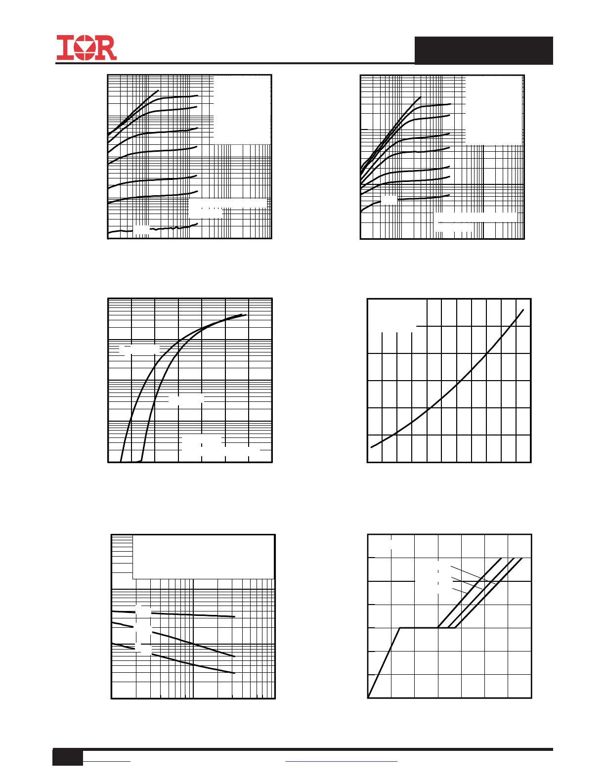
Fig 4. Normalized On-Resistance vs. Temperature
Fig 2. Typical Output Characteristics
Fig 1. Typical Output Characteristics
Fig 3. Typical Transfer Characteristics
Fig 6. Typical Gate Charge vs.Gate-to-Source Voltage
Fig 5. Typical Capacitance vs.Drain-to-Source Voltage
0.1
1
10
100
1000
VDS, Drain-to-Source Voltage (V)
0.1
1
10
100
1000
I D
, D
ra
in
-t
o-
S
ou
rc
e
C
ur
re
nt
(
A
)
VGS
TOP
10V
8.0V
7.0V
6.0V
5.5V
5.0V
4.8V
BOTTOM
4.5V
≤60μs PULSE WIDTH
Tj = 25°C
4.5V
0.1
1
10
100
1000
VDS, Drain-to-Source Voltage (V)
1
10
100
1000
I D
, D
ra
in
-t
o-
S
ou
rc
e
C
ur
re
nt
(
A
)
4.5V
≤60μs PULSE WIDTH
Tj = 150°C
VGS
TOP
10V
8.0V
7.0V
6.0V
5.5V
5.0V
4.8V
BOTTOM
4.5V
3
4
5
6
7
8
9
10
VGS, Gate-to-Source Voltage (V)
0.1
1
10
100
1000
I D
, D
ra
in
-t
o-
S
ou
rc
e
C
ur
re
nt
(
A
)
TJ = 25°C
TJ = 150°C
VDS = 15V
≤60μs PULSE WIDTH
-60 -40 -20 0 20 40 60 80 100 120 140 160
TJ , Junction Temperature (°C)
0.6
0.8
1.0
1.2
1.4
1.6
1.8
R
D
S
(o
n)
,
D
ra
in
-t
o-
S
ou
rc
e
O
n
R
es
is
ta
nc
e
(
N
or
m
al
iz
ed
)
ID = 50A
VGS = 10V
1
10
100
VDS, Drain-to-Source Voltage (V)
100
1000
10000
100000
C
, C
ap
ac
ita
nc
e
(p
F
)
VGS = 0V, f = 1 MHZ
Ciss = Cgs + Cgd, C ds SHORTED
Crss = Cgd
Coss = Cds + Cgd
Coss
Crss
Ciss
0
10
20
30
40
50
60
70
QG, Total Gate Charge (nC)
0.0
2.0
4.0
6.0
8.0
10.0
12.0
14.0
V
G
S
, G
at
e-
to
-S
ou
rc
e
V
ol
ta
ge
(
V
)
VDS= 32V
VDS= 20V
VDS= 8.0V
ID= 50A
4
www.irf.com
©
2015 International Rectifier
Submit Datasheet Feedback
March 16, 2015
IRFH5104PbF
Fig 11. Maximum Effective Transient Thermal Impedance, Junction-to-Case (Bottom)
Fig 8. Maximum Safe Operating Area
Fig 9. Maximum Drain Current vs.
Case (Bottom) Temperature
Fig 7. Typical Source-Drain Diode Forward Voltage
Fig 10. Threshold Voltage vs. Temperature
0.2
0.4
0.6
0.8
1.0
1.2
1.4
VSD, Source-to-Drain Voltage (V)
1.0
10
100
1000
I S
D
, R
ev
er
se
D
ra
in
C
ur
re
nt
(
A
)
TJ = 25°C
TJ = 150°C
VGS = 0V
0
1
10
100
VDS, Drain-to-Source Voltage (V)
1
10
100
1000
I D
,
D
ra
in
-t
o-
S
ou
rc
e
C
ur
re
nt
(
A
)
OPERATION IN THIS AREA
LIMITED BY R DS(on)
Tc = 25°C
Tj = 150°C
Single Pulse
100μsec
1msec
10msec
DC
25
50
75
100
125
150
TC , Case Temperature (°C)
0
25
50
75
100
125
150
I D
,
D
ra
in
C
ur
re
nt
(
A
)
Limited By Package
-75 -50 -25
0
25
50
75 100 125 150
TJ , Temperature ( °C )
1.5
2.0
2.5
3.0
3.5
4.0
4.5
5.0
V
G
S
(t
h)
, G
at
e
th
re
sh
ol
d
V
ol
ta
ge
(
V
)
ID = 100μA
ID = 500μA
ID = 1.0mA
ID = 1.0A
1E-006
1E-005
0.0001
0.001
0.01
0.1
t1 , Rectangular Pulse Duration (sec)
0.001
0.01
0.1
1
10
T
he
rm
al
R
es
po
ns
e
(
Z
th
JC
)
°
C
/W
0.20
0.10
D = 0.50
0.02
0.01
0.05
SINGLE PULSE
( THERMAL RESPONSE )
Notes:
1. Duty Factor D = t1/t2
2. Peak Tj = P dm x Zthjc + Tc
5
www.irf.com
©
2015 International Rectifier
Submit Datasheet Feedback
March 16, 2015
IRFH5104PbF
Fig 13. Maximum Avalanche Energy vs. Drain Current
Fig 12. On-Resistance vs. Gate Voltage
Fig 14b. Unclamped Inductive Waveforms
Fig 14a. Unclamped Inductive Test Circuit
tp
V
(BR)DSS
I
AS
RG
IAS
0.01
Ω
tp
D.U.T
L
VDS
+
- VDD
DRIVER
A
15V
20V
Fig 15a. Switching Time Test Circuit
Fig 15b. Switching Time Waveforms
V
GS
V
DS
90%
10%
t
d(on)
t
d(off)
t
r
t
f
V
DS
Pulse Width ≤ 1 µs
Duty Factor ≤ 0.1
R
D
V
GS
R
G
D.U.T.
10V
+
-
V
DD
V
GS
4
6
8
10
12
14
16
18
20
VGS, Gate -to -Source Voltage (V)
0
2
4
6
8
10
R
D
S
(o
n)
,
D
ra
in
-t
o
-S
ou
rc
e
O
n
R
es
is
ta
nc
e
(m
Ω
)
ID = 50A
TJ = 25°C
TJ = 125°C
25
50
75
100
125
150
Starting TJ , Junction Temperature (°C)
0
100
200
300
400
500
E
A
S
,
S
in
gl
e
P
ul
se
A
va
la
nc
he
E
ne
rg
y
(m
J)
ID
TOP 8.3A
19A
BOTTOM 50A
6
www.irf.com
©
2015 International Rectifier
Submit Datasheet Feedback
March 16, 2015
IRFH5104PbF
Fig 16.
Peak Diode Recovery dv/dt Test Circuit for N-Channel
HEXFET
®
Power MOSFETs
Fig 17. Gate Charge Test Circuit
Fig 18. Gate Charge Waveform
Vds
Vgs
Id
Vgs(th)
Qgs1 Qgs2
Qgd
Qgodr
Circuit Layout Considerations
• Low Stray Inductance
• Ground Plane
• Low Leakage Inductance
Current Transformer
P.W.
Period
di/dt
Diode Recovery
dv/dt
Ripple
≤ 5%
Body Diode Forward Drop
Re-Applied
Voltage
Reverse
Recovery
Current
Body Diode Forward
Current
V
GS
=10V
V
DD
I
SD
Driver Gate Drive
D.U.T. I
SD
Waveform
D.U.T. V
DS
Waveform
Inductor Curent
D =
P.W.
Period
*
V
GS
= 5V for Logic Level Devices
*
+
-
+
+
+
-
-
-
R
G
V
DD
• dv/dt controlled by R
G
• Driver same type as D.U.T.
• I
SD
controlled by Duty Factor "D"
• D.U.T. - Device Under Test
D.U.T
1K
VCC
DUT
0
L
S
7
www.irf.com
©
2015 International Rectifier
Submit Datasheet Feedback
March 16, 2015
IRFH5104PbF
Note: For the most current drawing please refer to IR website at:
http://www.irf.com/package/
XXXX
XYWWX
XXXXX
INTERNATIONAL
RECTIFIER LOGO
PART NUMBER
MARKING CODE
(Per Marking Spec)
ASSEMBLY
SITE CODE
(Per SCOP 200-002)
DATE CODE
PIN 1
IDENTIFIER
LOT CODE
(Eng Mode - Min last 4 digits of EATI#)
(Prod Mode - 4 digits of SPN code)
PQFN 5x6 Outline "B" Package Details
PQFN 5x6 Part Marking
For more information on board mounting, including footprint and stencil recommendation, please refer to application note AN-1136:
http://www.irf.com/technical-info/appnotes/an-1136.pdf
For more information on package inspection techniques, please refer to application note AN-1154:
http://www.irf.com/technical-info/appnotes/an-1154.pdf
8
www.irf.com
©
2015 International Rectifier
Submit Datasheet Feedback
March 16, 2015
IRFH5104PbF
PQFN 5x6 Tape and Reel
Bo
W
P 1
Ao
Ko
CODE
TAPE DIMENSIONS
REEL DIMENSIONS
QUADRANT ASSIGNMENTS FOR PIN 1 ORIENTATION IN TAPE
Dimension design to accommodate the component width
Dimension design to accommodate the component lenght
Dimension design to accommodate the component thickness
Pitch between successive cavity centers
Overall width of the carrier tape
DESCRIPTION
Type
Package
5 X 6 PQFN
Note: All dimension are nominal
Diameter
Reel
QTY
Width
Reel
(mm)
Ao
(mm)
Bo
(mm)
Ko
(mm)
P1
(mm)
W
Quadrant
Pin 1
(Inch)
W1
(mm)
13
4000
12.4
6.300
5.300
1.20
8.00
12
Q1
Note: For the most current drawing please refer to IR website at:
http://www.irf.com/package/
9
www.irf.com
©
2015 International Rectifier
Submit Datasheet Feedback
March 16, 2015
IRFH5104PbF
Qualification standards can be found at International Rectifier’s web site
http://www.irf.com/product-info/reliability
Higher qualification ratings may be available should the user have such requirements.
Please contact your International Rectifier sales representative for further information:
http://www.irf.com/whoto-call/salesrep/
Applicable version of JEDEC standard at the time of product release.
Notes:
Repetitive rating; pulse width limited by max. junction temperature.
Starting T
J
= 25°C, L = 0.098mH, R
G
= 25
Ω, I
AS
= 50A.
Pulse width ≤ 400μs; duty cycle ≤ 2%.
R
θ
is measured at T
J
of approximately 90°C.
When mounted on 1 inch square 2 oz copper pad on 1.5x1.5 in. board of FR-4 material.
Calculated continuous current based on maximum allowable junction temperature. Package is limited to 100A by production test
capability.
MS L1
(per JE DEC J-S T D-020D
†††
)
RoHS compliant
Yes
PQFN 5mm x 6mm
Qualification information
†
Moisture Sensitivity Level
Qualification level
Industrial
††
(per JE DEC JES D47F
†††
guidelines )
IR WORLD HEADQUARTERS: 101 N. Sepulveda Blvd., El Segundo, California 90245, USA
To contact International Rectifier, please visit
http://www.irf.com/whoto-call/
Revision History
Date
Comment
12/16/2013
• Updated ordering information to reflect the End-Of-Life (EOL) of the mini-reel option (EOL notice #259).
• Updated data sheet with the new IR corporate template.
3/16/2015
• Updated package outline and tape and reel on pages 7 and 8.
HEXFET
®
Power MOSFET
Notes
through
are on page 9
Features and Benefits
Applications
•
Secondary Side Synchronous Rectification
•
Inverters for DC Motors
•
DC-DC Brick Applications
•
Boost Converters
PQFN 5X6 mm
Absolute Maximum Ratings
Parameter
Units
V
DS
Drain-to-Source Voltage
V
GS
Gate-to-Source Voltage
I
D
@ T
A
= 25°C
Continuous Drain Current, V
GS
@ 10V
I
D
@ T
A
= 70°C
Continuous Drain Current, V
GS
@ 10V
I
D
@ T
C(Bottom)
= 25°C
Continuous Drain Current, V
GS
@ 10V
h
I
D
@ T
C(Bottom)
= 100°C
Continuous Drain Current, V
GS
@ 10V
I
DM
Pulsed Drain Current
c
P
D
@T
A
= 25°C
Power Dissipation g
P
D
@ T
C(Bottom)
= 25°C
Power Dissipation
g
Linear Derating Factor g
W/°C
T
J
Operating Junction and
T
STG
Storage Temperature Range
V
W
A
°C
Max.
24
86
400
±20
40
19
100
-55 to + 150
3.6
0.029
114
V
DS
40
V
R
DS(on) max
(@V
GS
= 10V)
3.5
m
Ω
Q
g (typical)
53
nC
R
G (typical)
1.4
Ω
I
D
(@T
c(Bottom)
= 25°C)
100h
A
Features
Benefits
Low R
DSon
(
≤ 3.5mΩ)
Lower Conduction Losses
Low Thermal Resistance to PCB (
≤ 1.1°C/W)
Enables better thermal dissipation
100% Rg tested
Increased Reliability
Low Profile (
≤ 0.9 mm)
results in Increased Power Density
Industry-Standard Pinout
⇒
Multi-Vendor Compatibility
Compatible with Existing Surface Mount Techniques
Easier Manufacturing
RoHS Compliant Containing no Lead, no Bromide and no Halogen
Environmentally Friendlier
MSL1, Industrial Qualification
Increased Reliability
IRFH5104PbF
1
www.irf.com
©
2015 International Rectifier
Submit Datasheet Feedback
March 16, 2015
Note
Form
Quantity
IRFH5104TRPBF
PQFN 5mm x 6mm
Tape and Reel
4000
IRFH5104TR2PBF
PQFN 5mm x 6mm
Tape and Reel
1000
EOL notice #259
Orderable part number
Package Type
Standard Pack
2
www.irf.com
©
2015 International Rectifier
Submit Datasheet Feedback
March 16, 2015
IRFH5104PbF
S
D
G
Thermal Resistance
Parameter
Typ.
Max.
Units
R
θJC
(Bottom)
Junction-to-Case f
–––
1.1
R
θJC
(Top)
Junction-to-Case
f
–––
15
°C/W
R
θJA
Junction-to-Ambient g
–––
35
R
θJA
(<10s)
Junction-to-Ambient
g
–––
22
Static @ T
J
= 25°C (unless otherwise specified)
Parameter
Min.
Typ.
Max. Units
BV
DSS
Drain-to-Source Breakdown Voltage
40
–––
–––
V
ΔΒV
DSS
/ΔT
J
Breakdown Voltage Temp. Coefficient
–––
0.05
–––
V/°C
R
DS(on)
Static Drain-to-Source On-Resistance
–––
2.9
3.5
V
GS(th)
Gate Threshold Voltage
2.0
–––
4.0
V
ΔV
GS(th)
Gate Threshold Voltage Coefficient
–––
-8.9
––– mV/°C
I
DSS
Drain-to-Source Leakage Current
–––
–––
20
–––
–––
250
I
GSS
Gate-to-Source Forward Leakage
–––
–––
100
Gate-to-Source Reverse Leakage
–––
–––
-100
gfs
Forward Transconductance
56
–––
–––
S
Q
g
Total Gate Charge
–––
53
80
Q
gs1
Pre-Vth Gate-to-Source Charge
–––
10
–––
Q
gs2
Post-Vth Gate-to-Source Charge
–––
4.8
–––
Q
gd
Gate-to-Drain Charge
–––
19
–––
Q
godr
Gate Charge Overdrive
–––
19.2
–––
See Fig.17 & 18
Q
sw
Switch Charge (Q
gs2
+ Q
gd
)
–––
23.8
–––
Q
oss
Output Charge
–––
22
–––
nC
R
G
Gate Resistance
–––
1.4
–––
Ω
t
d(on)
Turn-On Delay Time
–––
9.5
–––
t
r
Rise Time
–––
15
–––
t
d(off)
Turn-Off Delay Time
–––
20
–––
t
f
Fall Time
–––
10
–––
C
iss
Input Capacitance
–––
3120
–––
C
oss
Output Capacitance
–––
650
–––
C
rss
Reverse Transfer Capacitance
–––
310
–––
Avalanche Characteristics
Parameter
Units
E
AS
Single Pulse Avalanche Energy d
mJ
I
AR
Avalanche Current
c
A
Diode Characteristics
Parameter
Min.
Typ.
Max. Units
I
S
Continuous Source Current
(Body Diode) h
I
SM
Pulsed Source Current
(Body Diode)c
V
SD
Diode Forward Voltage
–––
–––
1.3
V
t
rr
Reverse Recovery Time
–––
31
47
ns
Q
rr
Reverse Recovery Charge
–––
130
195
nC
t
on
Forward Turn-On Time
Time is dominated by parasitic Inductance
V
DS
= V
GS
, I
D
= 100μA
A
100
–––
–––
400
–––
–––
nA
ns
pF
nC
Conditions
See Fig.15
Max.
120
50
ƒ = 1.0MHz
V
DS
= 20V
–––
Conditions
V
GS
= 0V, I
D
= 250μA
Reference to 25°C, I
D
= 1mA
V
GS
= 10V, I
D
= 50A e
MOSFET symbol
V
DS
= 16V, V
GS
= 0V
V
DD
= 20V, V
GS
= 10V
I
D
= 50A
V
GS
= 0V
V
DS
= 25V
V
GS
= 20V
V
GS
= -20V
V
DS
= 40V, V
GS
= 0V
T
J
= 25°C, I
F
= 50A, V
DD
= 20V
di/dt = 500A/μs
e
T
J
= 25°C, I
S
= 50A, V
GS
= 0V
e
showing the
integral reverse
p-n junction diode.
V
GS
= 10V
Typ.
–––
R
G
=1.7Ω
V
DS
= 15V, I
D
= 50A
V
DS
= 40V, V
GS
= 0V, T
J
= 125°C
m
Ω
μA
I
D
= 50A
3
www.irf.com
©
2015 International Rectifier
Submit Datasheet Feedback
March 16, 2015
IRFH5104PbF
Fig 4. Normalized On-Resistance vs. Temperature
Fig 2. Typical Output Characteristics
Fig 1. Typical Output Characteristics
Fig 3. Typical Transfer Characteristics
Fig 6. Typical Gate Charge vs.Gate-to-Source Voltage
Fig 5. Typical Capacitance vs.Drain-to-Source Voltage
0.1
1
10
100
1000
VDS, Drain-to-Source Voltage (V)
0.1
1
10
100
1000
I D
, D
ra
in
-t
o-
S
ou
rc
e
C
ur
re
nt
(
A
)
VGS
TOP
10V
8.0V
7.0V
6.0V
5.5V
5.0V
4.8V
BOTTOM
4.5V
≤60μs PULSE WIDTH
Tj = 25°C
4.5V
0.1
1
10
100
1000
VDS, Drain-to-Source Voltage (V)
1
10
100
1000
I D
, D
ra
in
-t
o-
S
ou
rc
e
C
ur
re
nt
(
A
)
4.5V
≤60μs PULSE WIDTH
Tj = 150°C
VGS
TOP
10V
8.0V
7.0V
6.0V
5.5V
5.0V
4.8V
BOTTOM
4.5V
3
4
5
6
7
8
9
10
VGS, Gate-to-Source Voltage (V)
0.1
1
10
100
1000
I D
, D
ra
in
-t
o-
S
ou
rc
e
C
ur
re
nt
(
A
)
TJ = 25°C
TJ = 150°C
VDS = 15V
≤60μs PULSE WIDTH
-60 -40 -20 0 20 40 60 80 100 120 140 160
TJ , Junction Temperature (°C)
0.6
0.8
1.0
1.2
1.4
1.6
1.8
R
D
S
(o
n)
,
D
ra
in
-t
o-
S
ou
rc
e
O
n
R
es
is
ta
nc
e
(
N
or
m
al
iz
ed
)
ID = 50A
VGS = 10V
1
10
100
VDS, Drain-to-Source Voltage (V)
100
1000
10000
100000
C
, C
ap
ac
ita
nc
e
(p
F
)
VGS = 0V, f = 1 MHZ
Ciss = Cgs + Cgd, C ds SHORTED
Crss = Cgd
Coss = Cds + Cgd
Coss
Crss
Ciss
0
10
20
30
40
50
60
70
QG, Total Gate Charge (nC)
0.0
2.0
4.0
6.0
8.0
10.0
12.0
14.0
V
G
S
, G
at
e-
to
-S
ou
rc
e
V
ol
ta
ge
(
V
)
VDS= 32V
VDS= 20V
VDS= 8.0V
ID= 50A
4
www.irf.com
©
2015 International Rectifier
Submit Datasheet Feedback
March 16, 2015
IRFH5104PbF
Fig 11. Maximum Effective Transient Thermal Impedance, Junction-to-Case (Bottom)
Fig 8. Maximum Safe Operating Area
Fig 9. Maximum Drain Current vs.
Case (Bottom) Temperature
Fig 7. Typical Source-Drain Diode Forward Voltage
Fig 10. Threshold Voltage vs. Temperature
0.2
0.4
0.6
0.8
1.0
1.2
1.4
VSD, Source-to-Drain Voltage (V)
1.0
10
100
1000
I S
D
, R
ev
er
se
D
ra
in
C
ur
re
nt
(
A
)
TJ = 25°C
TJ = 150°C
VGS = 0V
0
1
10
100
VDS, Drain-to-Source Voltage (V)
1
10
100
1000
I D
,
D
ra
in
-t
o-
S
ou
rc
e
C
ur
re
nt
(
A
)
OPERATION IN THIS AREA
LIMITED BY R DS(on)
Tc = 25°C
Tj = 150°C
Single Pulse
100μsec
1msec
10msec
DC
25
50
75
100
125
150
TC , Case Temperature (°C)
0
25
50
75
100
125
150
I D
,
D
ra
in
C
ur
re
nt
(
A
)
Limited By Package
-75 -50 -25
0
25
50
75 100 125 150
TJ , Temperature ( °C )
1.5
2.0
2.5
3.0
3.5
4.0
4.5
5.0
V
G
S
(t
h)
, G
at
e
th
re
sh
ol
d
V
ol
ta
ge
(
V
)
ID = 100μA
ID = 500μA
ID = 1.0mA
ID = 1.0A
1E-006
1E-005
0.0001
0.001
0.01
0.1
t1 , Rectangular Pulse Duration (sec)
0.001
0.01
0.1
1
10
T
he
rm
al
R
es
po
ns
e
(
Z
th
JC
)
°
C
/W
0.20
0.10
D = 0.50
0.02
0.01
0.05
SINGLE PULSE
( THERMAL RESPONSE )
Notes:
1. Duty Factor D = t1/t2
2. Peak Tj = P dm x Zthjc + Tc
5
www.irf.com
©
2015 International Rectifier
Submit Datasheet Feedback
March 16, 2015
IRFH5104PbF
Fig 13. Maximum Avalanche Energy vs. Drain Current
Fig 12. On-Resistance vs. Gate Voltage
Fig 14b. Unclamped Inductive Waveforms
Fig 14a. Unclamped Inductive Test Circuit
tp
V
(BR)DSS
I
AS
RG
IAS
0.01
Ω
tp
D.U.T
L
VDS
+
- VDD
DRIVER
A
15V
20V
Fig 15a. Switching Time Test Circuit
Fig 15b. Switching Time Waveforms
V
GS
V
DS
90%
10%
t
d(on)
t
d(off)
t
r
t
f
V
DS
Pulse Width ≤ 1 µs
Duty Factor ≤ 0.1
R
D
V
GS
R
G
D.U.T.
10V
+
-
V
DD
V
GS
4
6
8
10
12
14
16
18
20
VGS, Gate -to -Source Voltage (V)
0
2
4
6
8
10
R
D
S
(o
n)
,
D
ra
in
-t
o
-S
ou
rc
e
O
n
R
es
is
ta
nc
e
(m
Ω
)
ID = 50A
TJ = 25°C
TJ = 125°C
25
50
75
100
125
150
Starting TJ , Junction Temperature (°C)
0
100
200
300
400
500
E
A
S
,
S
in
gl
e
P
ul
se
A
va
la
nc
he
E
ne
rg
y
(m
J)
ID
TOP 8.3A
19A
BOTTOM 50A
6
www.irf.com
©
2015 International Rectifier
Submit Datasheet Feedback
March 16, 2015
IRFH5104PbF
Fig 16.
Peak Diode Recovery dv/dt Test Circuit for N-Channel
HEXFET
®
Power MOSFETs
Fig 17. Gate Charge Test Circuit
Fig 18. Gate Charge Waveform
Vds
Vgs
Id
Vgs(th)
Qgs1 Qgs2
Qgd
Qgodr
Circuit Layout Considerations
• Low Stray Inductance
• Ground Plane
• Low Leakage Inductance
Current Transformer
P.W.
Period
di/dt
Diode Recovery
dv/dt
Ripple
≤ 5%
Body Diode Forward Drop
Re-Applied
Voltage
Reverse
Recovery
Current
Body Diode Forward
Current
V
GS
=10V
V
DD
I
SD
Driver Gate Drive
D.U.T. I
SD
Waveform
D.U.T. V
DS
Waveform
Inductor Curent
D =
P.W.
Period
*
V
GS
= 5V for Logic Level Devices
*
+
-
+
+
+
-
-
-
R
G
V
DD
• dv/dt controlled by R
G
• Driver same type as D.U.T.
• I
SD
controlled by Duty Factor "D"
• D.U.T. - Device Under Test
D.U.T
1K
VCC
DUT
0
L
S
7
www.irf.com
©
2015 International Rectifier
Submit Datasheet Feedback
March 16, 2015
IRFH5104PbF
Note: For the most current drawing please refer to IR website at:
http://www.irf.com/package/
XXXX
XYWWX
XXXXX
INTERNATIONAL
RECTIFIER LOGO
PART NUMBER
MARKING CODE
(Per Marking Spec)
ASSEMBLY
SITE CODE
(Per SCOP 200-002)
DATE CODE
PIN 1
IDENTIFIER
LOT CODE
(Eng Mode - Min last 4 digits of EATI#)
(Prod Mode - 4 digits of SPN code)
PQFN 5x6 Outline "B" Package Details
PQFN 5x6 Part Marking
For more information on board mounting, including footprint and stencil recommendation, please refer to application note AN-1136:
http://www.irf.com/technical-info/appnotes/an-1136.pdf
For more information on package inspection techniques, please refer to application note AN-1154:
http://www.irf.com/technical-info/appnotes/an-1154.pdf
8
www.irf.com
©
2015 International Rectifier
Submit Datasheet Feedback
March 16, 2015
IRFH5104PbF
PQFN 5x6 Tape and Reel
Bo
W
P 1
Ao
Ko
CODE
TAPE DIMENSIONS
REEL DIMENSIONS
QUADRANT ASSIGNMENTS FOR PIN 1 ORIENTATION IN TAPE
Dimension design to accommodate the component width
Dimension design to accommodate the component lenght
Dimension design to accommodate the component thickness
Pitch between successive cavity centers
Overall width of the carrier tape
DESCRIPTION
Type
Package
5 X 6 PQFN
Note: All dimension are nominal
Diameter
Reel
QTY
Width
Reel
(mm)
Ao
(mm)
Bo
(mm)
Ko
(mm)
P1
(mm)
W
Quadrant
Pin 1
(Inch)
W1
(mm)
13
4000
12.4
6.300
5.300
1.20
8.00
12
Q1
Note: For the most current drawing please refer to IR website at:
http://www.irf.com/package/
9
www.irf.com
©
2015 International Rectifier
Submit Datasheet Feedback
March 16, 2015
IRFH5104PbF
Qualification standards can be found at International Rectifier’s web site
http://www.irf.com/product-info/reliability
Higher qualification ratings may be available should the user have such requirements.
Please contact your International Rectifier sales representative for further information:
http://www.irf.com/whoto-call/salesrep/
Applicable version of JEDEC standard at the time of product release.
Notes:
Repetitive rating; pulse width limited by max. junction temperature.
Starting T
J
= 25°C, L = 0.098mH, R
G
= 25
Ω, I
AS
= 50A.
Pulse width ≤ 400μs; duty cycle ≤ 2%.
R
θ
is measured at T
J
of approximately 90°C.
When mounted on 1 inch square 2 oz copper pad on 1.5x1.5 in. board of FR-4 material.
Calculated continuous current based on maximum allowable junction temperature. Package is limited to 100A by production test
capability.
MS L1
(per JE DEC J-S T D-020D
†††
)
RoHS compliant
Yes
PQFN 5mm x 6mm
Qualification information
†
Moisture Sensitivity Level
Qualification level
Industrial
††
(per JE DEC JES D47F
†††
guidelines )
IR WORLD HEADQUARTERS: 101 N. Sepulveda Blvd., El Segundo, California 90245, USA
To contact International Rectifier, please visit
http://www.irf.com/whoto-call/
Revision History
Date
Comment
12/16/2013
• Updated ordering information to reflect the End-Of-Life (EOL) of the mini-reel option (EOL notice #259).
• Updated data sheet with the new IR corporate template.
3/16/2015
• Updated package outline and tape and reel on pages 7 and 8.