
Strong
IR
FET™
IRFB7434PbF
HEXFET
®
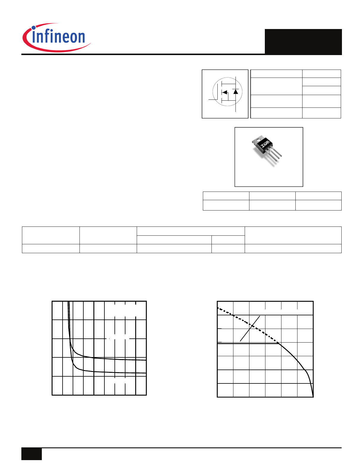
Power MOSFET
D
S
G
Application
Brushed Motor drive applications
BLDC Motor drive applications
Battery powered circuits
Half-bridge and full-bridge topologies
Synchronous rectifier applications
Resonant mode power supplies
OR-ing and redundant power switches
DC/DC and AC/DC converters
DC/AC Inverters
Benefits
Improved Gate, Avalanche and Dynamic dV/dt Ruggedness
Fully Characterized Capacitance and Avalanche SOA
Enhanced body diode dV/dt and dI/dt Capability
Lead-Free*
RoHS Compliant, Halogen-Free*
V
DSS
40V
R
DS(on)
typ.
1.25m
max
1.6m
I
D (Silicon Limited)
317A
I
D (Package Limited)
195A
Fig 1. Typical On-Resistance vs. Gate Voltage
Fig 2. Maximum Drain Current vs. Case Temperature
TO-220AB
IRFB7434PbF
S
D
G
G D S
Gate Drain Source
Base part number
Package Type
Standard Pack
Orderable Part Number
Form
Quantity
IRFB7434PbF
TO-220
Tube
50
IRFB7434PbF
1
2018-07-10
2
4
6
8
10
12
14
16
18
20
VGS, Gate -to -Source Voltage (V)
0
1
2
3
4
5
R
D
S
(o
n)
,
D
ra
in
-t
o
-S
ou
rc
e
O
n
R
es
is
ta
nc
e
(
m
)
ID = 100A
TJ = 25°C
TJ = 125°C
25
50
75
100
125
150
175
TC , Case Temperature (°C)
0
50
100
150
200
250
300
350
I D
,
D
ra
in
C
ur
re
nt
(
A
)
Limited By Package
2
2018-07-10
IRFB7434PbF
Absolute Maximum Rating
Symbol
Parameter Max.
Units
I
D
@ T
C
= 25°C
Continuous Drain Current, VGS @ 10V (Silicon Limited)
317
A
I
D
@ T
C
= 100°C
Continuous Drain Current, V
GS
@ 10V (Silicon Limited)
224
I
D
@ T
C
= 25°C
Continuous Drain Current, V
GS
@ 10V (Wire Bond Limited)
195
I
DM
Pulsed Drain Current
1270
P
D
@T
C
= 25°C
Maximum Power Dissipation
294
W
Linear Derating Factor
1.96
W/°C
V
GS
Gate-to-Source Voltage
± 20
V
T
J
T
STG
Operating Junction and
Storage Temperature Range
-55 to + 175
°C
Soldering Temperature, for 10 seconds (1.6mm from case)
300
Mounting Torque, 6-32 or M3 Screw
10 lbf·in (1.1 N·m)
Avalanche Characteristics
E
AS (Thermally limited)
Single Pulse Avalanche Energy
490
mJ
E
AS (Thermally limited)
Single Pulse Avalanche Energy
1098
I
AR
Avalanche Current
See Fig 15, 16, 23a, 23b
A
E
AR
Repetitive Avalanche Energy mJ
Thermal Resistance
Symbol
Parameter Typ.
Max.
Units
R
JC
Junction-to-Case
––– 0.51
°C/W
R
CS
Case-to-Sink, Flat Greased Surface
0.50 –––
R
JA
Junction-to-Ambient
––– 62
Static @ T
J
= 25°C (unless otherwise specified)
Symbol
Parameter Min.
Typ.
Max.
Units
Conditions
V
(BR)DSS
Drain-to-Source Breakdown Voltage
40
––– –––
V
V
GS
= 0V, I
D
= 250µA
V
(BR)DSS
/
T
J
Breakdown Voltage Temp. Coefficient
––– 0.032 –––
V/°C Reference to 25°C, I
D
= 5mA
R
DS(on)
––– 1.25 1.6
m
V
GS
= 10V, I
D
= 100A
––– 1.8 –––
V
GS
= 6.0V, I
D
= 50A
V
GS(th)
Gate Threshold Voltage
2.2
3.0
3.9
V
V
DS
= V
GS
, I
D
= 250µA
I
DSS
Drain-to-Source Leakage Current
––– ––– 1.0
µA
V
DS
=40 V, V
GS
= 0V
––– ––– 150
V
DS
=40V,V
GS
= 0V,T
J
=125°C
I
GSS
Gate-to-Source Forward Leakage
–––
––– 100
nA
V
GS
= 20V
Gate-to-Source Reverse Leakage
–––
––– -100
V
GS
= -20V
R
G
Gate Resistance
–––
2.1
–––
Static Drain-to-Source On-Resistance
Notes:
Calculated continuous current based on maximum allowable junction temperature. Bond wire current limit is 195A. Note that current
limitations arising from heating of the device leads may occur with some lead mounting arrangements. (Refer to AN-1140)
Repetitive rating; pulse width limited by max. junction temperature.
Limited by T
Jmax
, starting T
J
= 25°C, L = 0.099mH,R
G
= 50
, I
AS
= 100A, V
GS
=10V.
I
SD
100A, di/dt 1307A/µs, V
DD
V
(BR)DSS
, T
J
175°C.
Pulse width
400µs; duty cycle 2%.
C
oss
eff. (TR) is a fixed capacitance that gives the same charging time as C
oss
while V
DS
is rising from 0 to 80% V
DSS
.
C
oss
eff. (ER) is a fixed capacitance that gives the same energy as C
oss
while VDS is rising from 0 to 80% V
DSS
.
R
is measured at T
J
approximately 90°C.
Limited by T
Jmax
, starting T
J
= 25°C, L= 1mH, R
G
= 50
, I
AS
= 47A, V
GS
=10V.
*
Halogen -Free since April 30, 2014
3
2018-07-10
IRFB7434PbF
Dynamic Electrical Characteristics @ T
J
= 25°C (unless otherwise specified)
Symbol
Parameter Min.
Typ.
Max.
Units
Conditions
gfs Forward
Transconductance
211
–––
–––
S
V
DS
= 10V, I
D
=100A
Q
g
Total Gate Charge
–––
216
324
I
D
= 100A
Q
gs
Gate-to-Source Charge
–––
51
–––
V
DS
= 20V
Q
gd
Gate-to-Drain Charge
–––
77
–––
V
GS
= 10V
Q
sync
Total Gate Charge Sync. (Qg– Qgd)
–––
139
–––
t
d(on)
Turn-On Delay Time
–––
24
–––
ns
V
DD
= 20V
t
r
Rise Time
–––
68
–––
I
D
= 30A
t
d(off)
Turn-Off Delay Time
–––
115
–––
R
G
= 2.7
t
f
Fall Time
–––
68
–––
V
GS
= 10V
C
iss
Input Capacitance
––– 10820 –––
pF
V
GS
= 0V
C
oss
Output Capacitance
–––
1540
–––
V
DS
= 25V
C
rss
Reverse Transfer Capacitance
–––
1140
–––
ƒ = 1.0MHz, See Fig.5
C
oss eff.(ER)
Effective Output Capacitance
(Energy Related)
––– 1880 –––
V
GS
= 0V, VDS = 0V to 32V
C
oss eff.(TR)
Output Capacitance (Time Related)
–––
2208
–––
V
GS
= 0V, VDS = 0V to 32V
Diode Characteristics
Symbol
Parameter Min.
Typ.
Max.
Units
Conditions
I
S
Continuous Source Current
––– ––– 317
A
MOSFET symbol
(Body Diode)
showing the
I
SM
Pulsed Source Current
––– ––– 1270
integral reverse
(Body Diode)
p-n junction diode.
V
SD
Diode Forward Voltage
–––
0.9
1.3
V T
J
= 25°C,I
S
= 100A,V
GS
= 0V
dv/dt
Peak Diode Recovery dv/dt
––– 5.0 –––
V/ns
T
J
= 175°C,I
S
= 100A,V
DS
= 40V
t
rr
Reverse Recovery Time
––– 38 –––
ns
T
J
= 25°C V
DD
= 34V
––– 37 –––
T
J
= 125°C I
F
= 100A,
Q
rr
Reverse Recovery Charge
––– 50 –––
nC
T
J
= 25°C di/dt = 100A/µs
––– 50 –––
T
J
= 125°C
I
RRM
Reverse Recovery Current
–––
1.9
–––
A T
J
= 25°C
nC
D
S
G
4
2018-07-10
IRFB7434PbF
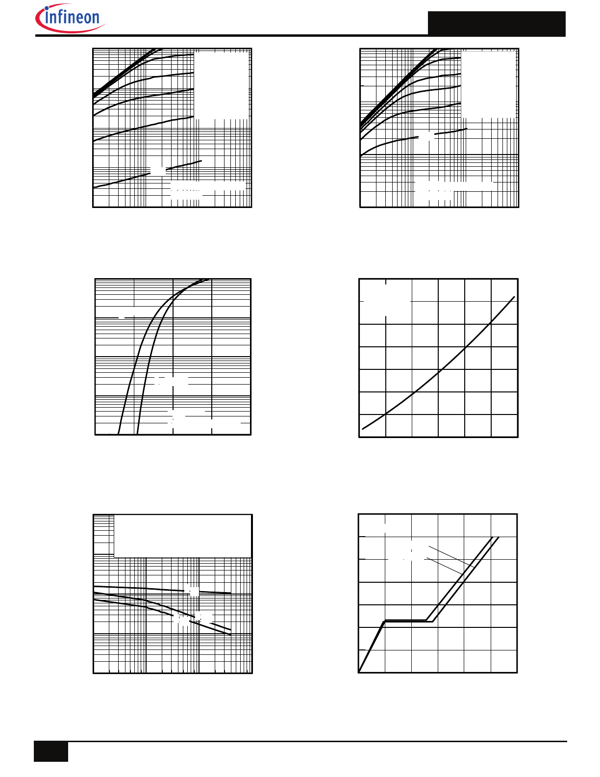
Fig 6. Normalized On-Resistance vs. Temperature
Fig 5. Typical Transfer Characteristics
Fig 4. Typical Output Characteristics
Fig 3. Typical Output Characteristics
Fig 7. Typical Capacitance vs. Drain-to-Source Voltage
0.1
1
10
100
VDS, Drain-to-Source Voltage (V)
0.1
1
10
100
1000
I D
,
D
ra
in
-t
o
-S
ou
rc
e
C
u
rr
e
nt
(
A
)
VGS
TOP 15V
10V
8.0V
7.0V
6.0V
5.5V
5.0V
BOTTOM
4.5V
60µs
PULSE WIDTH
Tj = 25°C
4.5V
2
4
6
8
10
VGS, Gate-to-Source Voltage (V)
0.1
1
10
100
1000
I D
, D
ra
in
-t
o-
S
ou
rc
e
C
ur
re
nt
(A
)
TJ = 25°C
TJ = 175°C
VDS = 10V
60µs PULSE WIDTH
0.1
1
10
100
VDS, Drain-to-Source Voltage (V)
100
1000
10000
100000
1000000
C
, C
ap
ac
ita
nc
e
(p
F
)
VGS = 0V, f = 1 MHZ
Ciss = Cgs + Cgd, C ds SHORTED
Crss = Cgd
Coss = Cds + Cgd
Coss
Crss
Ciss
0.1
1
10
100
VDS, Drain-to-Source Voltage (V)
1
10
100
1000
I D
, D
ra
in
-t
o-
S
o
ur
ce
C
u
rr
en
t (
A
)
4.5V
60µs
PULSE WIDTH
Tj = 175°C
VGS
TOP 15V
10V
8.0V
7.0V
6.0V
5.5V
5.0V
BOTTOM
4.5V
-60
-20
20
60
100
140
180
TJ , Junction Temperature (°C)
0.6
0.8
1.0
1.2
1.4
1.6
1.8
2.0
R
D
S
(o
n)
,
D
ra
in
-t
o-
S
ou
rc
e
O
n
R
es
is
ta
nc
e
(
N
or
m
al
iz
ed
)
ID = 100A
VGS = 10V
0
50
100
150
200
250
300
QG, Total Gate Charge (nC)
0.0
2.0
4.0
6.0
8.0
10.0
12.0
14.0
V
G
S
, G
at
e-
to
-S
ou
rc
e
V
ol
ta
ge
(
V
)
VDS= 32V
VDS= 20V
ID= 100A
Fig 8. Typical Gate Charge vs.
Gate-to-Source Voltage
5
2018-07-10
IRFB7434PbF
Fig 10. Maximum Safe Operating Area
Fig 9. Typical Source-Drain Diode Forward Voltage
Fig 12. Typical C
oss
Stored Energy
Fig 13. Typical On-Resistance vs. Drain Current
Fig 11. Drain-to-Source Breakdown Voltage
0.0
0.5
1.0
1.5
2.0
2.5
VSD, Source-to-Drain Voltage (V)
0.1
1
10
100
1000
I S
D
, R
ev
er
se
D
ra
in
C
ur
re
nt
(
A
)
TJ = 25°C
TJ = 175°C
VGS = 0V
-60
-20
20
60
100
140
180
TJ , Temperature ( °C )
40
41
42
43
44
45
46
47
48
49
50
V
(B
R
)D
S
S
, D
ra
in
-t
o-
S
ou
rc
e
B
re
ak
do
w
n
V
ol
ta
ge
(
V
)
Id = 5.0mA
0
100
200
300
400
500
ID, Drain Current (A)
0.0
5.0
10.0
15.0
20.0
R
D
S
(o
n)
,
D
ra
in
-t
o
-S
ou
rc
e
O
n
R
es
is
ta
nc
e
(m
)
VGS = 7.0V
VGS = 8.0V
VGS = 10V
VGS = 6.0V
VGS = 5.5V
0
5
10
15
20
25
30
35
40
45
VDS, Drain-to-Source Voltage (V)
0.0
0.2
0.4
0.6
0.8
1.0
1.2
1.4
1.6
E
ne
rg
y
(µ
J)
VDS= 0V to 32V
0.1
1
10
100
VDS, Drain-to-Source Voltage (V)
0.1
1
10
100
1000
10000
I D
,
D
ra
in
-t
o-
S
ou
rc
e
C
ur
re
nt
(
A
)
Tc = 25°C
Tj = 175°C
Single Pulse
10msec
1msec
OPERATION IN THIS AREA
LIMITED BY RDS(on)
100µsec
DC
Limited By Package
6
2018-07-10
IRFB7434PbF
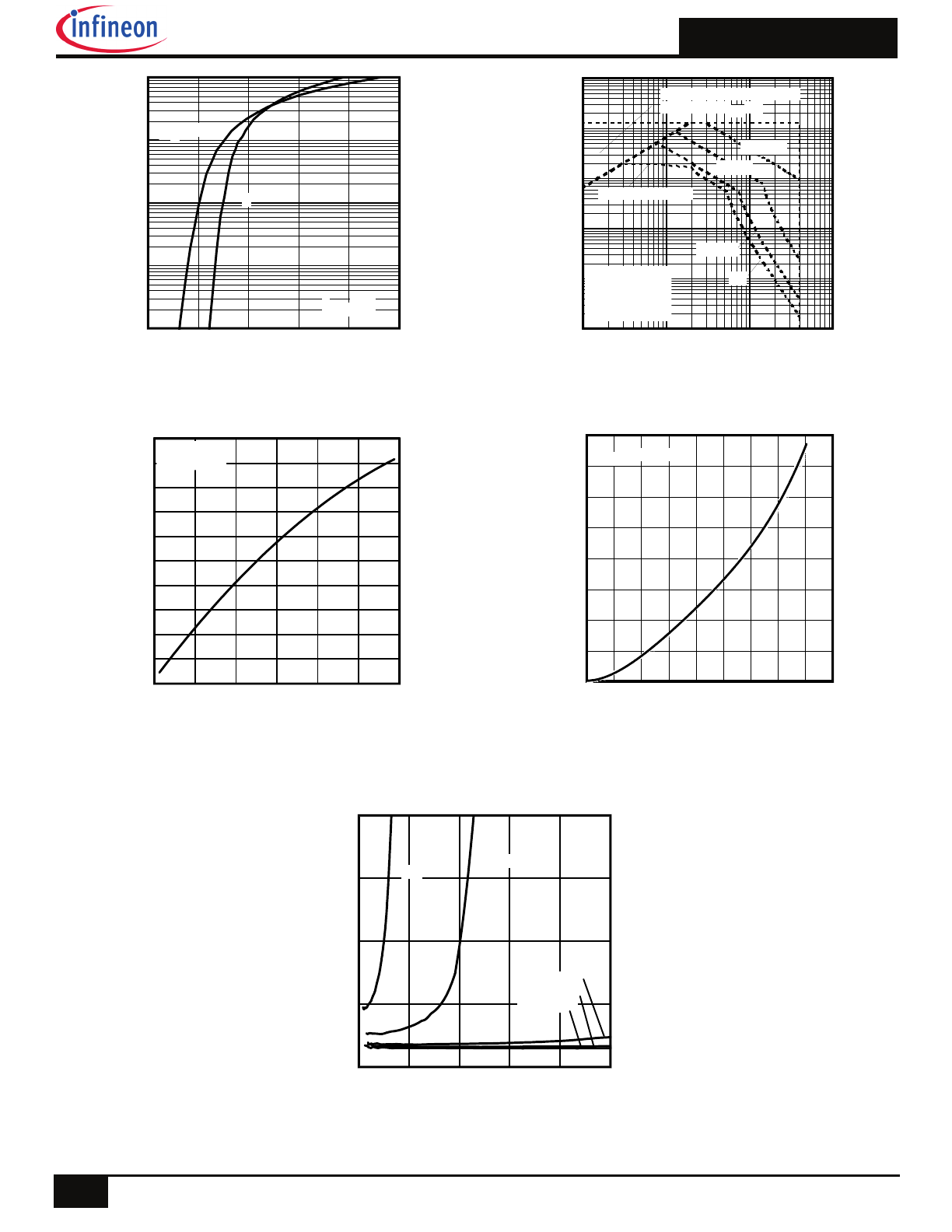
Fig 14. Maximum Effective Transient Thermal Impedance, Junction-to-Case
Fig 16.
Maximum Avalanche Energy vs. Temperature
Notes on Repetitive Avalanche Curves , Figures 15, 16:
(For further info, see AN-1005 at www.irf.com)
1.Avalanche failures assumption:
Purely a thermal phenomenon and failure occurs at a
temperature far in excess of T
jmax
. This is validated for every
part
type.
2. Safe operation in Avalanche is allowed as long asT
jmax
is not
exceeded.
3. Equation below based on circuit and waveforms shown in Figures
23a, 23b.
4. P
D (ave)
= Average power dissipation per single avalanche pulse.
5. BV = Rated breakdown voltage (1.3 factor accounts for voltage
increase during avalanche).
6. I
av
= Allowable avalanche current.
7.
T = Allowable rise in junction temperature, not to exceed T
jmax
(assumed as 25°C in Figure 14, 15).
t
av
= Average time in avalanche.
D = Duty cycle in avalanche = tav ·f
Z
thJC
(D, t
av
) = Transient thermal resistance, see Figures 14)
PD (ave) = 1/2 ( 1.3·BV·I
av
) =
T/ Z
thJC
I
av
= 2
T/ [1.3·BV·Z
th
]
E
AS (AR)
= P
D (ave)·
t
av
Fig 15. Avalanche Current vs. Pulse Width
1E-006
1E-005
0.0001
0.001
0.01
0.1
t1 , Rectangular Pulse Duration (sec)
0.0001
0.001
0.01
0.1
1
T
he
rm
al
R
es
po
ns
e
(
Z
th
JC
)
°
C
/W
0.20
0.10
D = 0.50
0.02
0.01
0.05
SINGLE PULSE
( THERMAL RESPONSE )
Notes:
1. Duty Factor D = t1/t2
2. Peak Tj = P dm x Zthjc + Tc
1.0E-06
1.0E-05
1.0E-04
1.0E-03
1.0E-02
1.0E-01
tav (sec)
1
10
100
1000
A
va
la
nc
he
C
ur
re
nt
(
A
)
Allowed avalanche Current vs avalanche
pulsewidth, tav, assuming j = 25°C and
Tstart = 150°C.
Allowed avalanche Current vs avalanche
pulsewidth, tav, assuming Tj = 150°C and
Tstart =25°C (Single Pulse)
25
50
75
100
125
150
175
Starting TJ , Junction Temperature (°C)
0
100
200
300
400
500
600
E
A
R
,
A
va
la
nc
he
E
ne
rg
y
(m
J)
TOP Single Pulse
BOTTOM 1.0% Duty Cycle
ID = 100A
7
2018-07-10
IRFB7434PbF
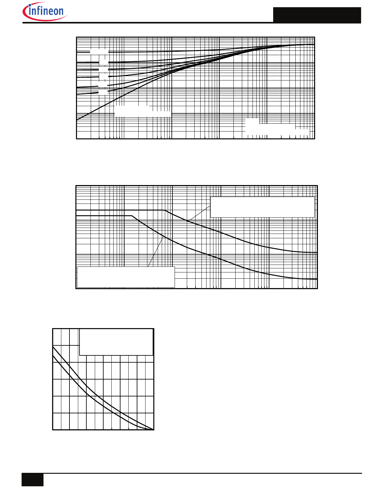
Fig 17. Threshold Voltage vs. Temperature
Fig 19. Typical Recovery Current vs. dif/dt
Fig 20. Typical Stored Charge vs. dif/dt
Fig 21. Typical Stored Charge vs. dif/dt
-75
-25
25
75
125
175
225
TJ , Temperature ( °C )
0.5
1.5
2.5
3.5
4.5
V
G
S
(t
h)
, G
at
e
th
re
sh
ol
d
V
ol
ta
ge
(
V
)
ID = 250µA
ID = 1.0mA
ID = 1.0A
0
200
400
600
800
1000
diF /dt (A/µs)
0
2
4
6
8
10
I R
R
M
(
A
)
IF = 60A
VR = 34V
TJ = 25°C
TJ = 125°C
0
200
400
600
800
1000
diF /dt (A/µs)
0
2
4
6
8
10
I R
R
M
(
A
)
IF = 100A
VR = 34V
TJ = 25°C
TJ = 125°C
0
200
400
600
800
1000
diF /dt (A/µs)
40
60
80
100
120
140
160
180
200
220
240
Q
R
R
(
nC
)
IF = 60A
VR = 34V
TJ = 25°C
TJ = 125°C
Fig 18. Typical Recovery Current vs. dif/dt
0
200
400
600
800
1000
diF /dt (A/µs)
0
40
80
120
160
200
Q
R
R
(
nC
)
IF = 100A
VR = 34V
TJ = 25°C
TJ = 125°C
8
2018-07-10
IRFB7434PbF
Fig 22. Peak Diode Recovery dv/dt Test Circuit for N-Channel HEXFET
®
Power MOSFETs
Fig 23a. Unclamped Inductive Test Circuit
R G
I
AS
0.01
tp
D.U.T
L
VDS
+
- VDD
DRIVER
A
15V
20V
Fig 24a. Switching Time Test Circuit
Fig 25a. Gate Charge Test Circuit
tp
V
(BR)DSS
I
AS
Fig 23b. Unclamped Inductive Waveforms
Fig 24b. Switching Time Waveforms
Vds
Vgs
Id
Vgs(th)
Qgs1 Qgs2
Qgd
Qgodr
Fig 25b. Gate Charge Waveform
VDD
9
2018-07-10
IRFB7434PbF
TO-220AB Package Outline (Dimensions are shown in millimeters (inches))
TO-220AB Part Marking Information
IN T E R N A T IO N A L
P A R T N U M B E R
R E C T IF IE R
L O T C O D E
A S S E M B L Y
L O G O
Y E A R 0 = 2 0 0 0
D A T E C O D E
W E E K 1 9
L IN E C
L O T C O D E 1 7 8 9
E X A M P L E : T H IS IS A N IR F 1 0 1 0
N o t e : " P " in a s s e m b ly lin e p o s it io n
in d ic a t e s " L e a d - F r e e "
IN T H E A S S E M B L Y L IN E " C "
A S S E M B L E D O N W W 1 9 , 2 0 0 0
TO-220AB packages are not recommended for Surface Mount Application
.
10
2018-07-10
IRFB7434PbF
† Applicable version of JEDEC standard at the time of product release.
Qualification Information
Qualification Level
Industrial
(per JEDEC JESD47F)
†
Moisture Sensitivity Level
TO-220 N/A
RoHS Compliant
Yes
Revision History
Date Comment
4/22/2014
Updated data sheet with new IR corporate template.
Updated package outline and part marking on page 9.
Added bullet point in the Benefits "RoHS Compliant, Halogen -Free" on page 1.
11/18/2014
Updated E
AS
(L =1mH)
= 1098mJ on page 2
Updated note 9 “Limited by T
Jmax
, starting T
J
= 25°C, L = 1mH, R
G
= 50
, I
AS
= 47A, V
GS
=10V”. on page 2
07/10/2018
Updated datasheet with corporate template.
Corrected typo for Fig 10 (package limit from 10ms curve to DC curve) –on page 5
Trademarks of Infineon Technologies AG
µHVIC™, µIPM™, µPFC™, AU-ConvertIR™, AURIX™, C166™, CanPAK™, CIPOS™, CIPURSE™, CoolDP™, CoolGaN™, COOLiR™, CoolMOS™, CoolSET™, CoolSiC™,
DAVE™, DI-POL™, DirectFET™, DrBlade™, EasyPIM™, EconoBRIDGE™, EconoDUAL™, EconoPACK™, EconoPIM™, EiceDRIVER™, eupec™, FCOS™, GaNpowIR™,
HEXFET™, HITFET™, HybridPACK™, iMOTION™, IRAM™, ISOFACE™, IsoPACK™, LEDrivIR™, LITIX™, MIPAQ™, ModSTACK™, my-d™, NovalithIC™, OPTIGA™,
OptiMOS™, ORIGA™, PowIRaudio™, PowIRStage™, PrimePACK™, PrimeSTACK™, PROFET™, PRO-SIL™, RASIC™, REAL3™, SmartLEWIS™, SOLID FLASH™, SPOC™,
StrongIRFET™, SupIRBuck™, TEMPFET™, TRENCHSTOP™, TriCore™, UHVIC™, XHP™, XMC™
Trademarks updated November 2015
Other Trademarks
All referenced product or service names and trademarks are the property of their respective owners.
Edition 2016-04-19
Published by
Infineon Technologies AG
81726 Munich, Germany
© 2016 Infineon Technologies AG.
All Rights Reserved.
Do you have a question about this
document?
Email:
erratum@infineon.com
Document reference
ifx1
IMPORTANT NOTICE
The information given in this document shall in no event
be regarded as a guarantee of conditions or
characteristics (“Beschaffenheitsgarantie”) .
With respect to any examples, hints or any typical values
stated herein and/or any information regarding the
application of the product, Infineon Technologies
hereby disclaims any and all warranties and liabilities of
any kind, including without limitation warranties of non-
infringement of intellectual property rights of any third
party.
In addition, any information given in this document is
subject to customer’s compliance with its obligations
stated in this document and any applicable legal
requirements, norms and standards concerning
customer’s products and any use of the product of
Infineon Technologies in customer’s applications.
The data contained in this document is exclusively
intended for technically trained staff. It is the
responsibility of customer’s technical departments
to evaluate the suitability of the product for the
intended application and the completeness of the
product information given in this document with respect
to such application.
For further information on the product, technology,
delivery terms and conditions and prices please contact
your nearest Infineon Technologies office
(
www.infineon.com
).
Please note that this product is not qualified according to
the AEC Q100 or AEC Q101 documents of the Automotive
Electronics Council.
WARNINGS
Due to technical requirements products may contain
dangerous substances. For information on the types in
question please contact your nearest Infineon
Technologies office.
Except as otherwise explicitly approved by Infineon
Technologies in a written document signed by authorized
representatives of Infineon Technologies, Infineon
Technologies’ products may not be used in any
applications where a failure of the product or any
consequences of the use thereof can reasonably be
expected to result in personal injury.