
IRFB4137PbF
1
www.irf.com
© 2012 International Rectifier
October 30, 2012
HEXFET
®
Power MOSFET
D
S
G
TO-220Pak
G D S
Gate Drain Source
Application
High Efficiency Synchronous Rectification in SMPS
Uninterruptible Power Supply
High Speed Power Switching
Hard Switched and High Frequency Circuits
Benefits
Improved Gate, Avalanche and Dynamic dV/dt Ruggedness
Fully Characterized Capacitance and Avalanche SOA
Enhanced body diode dV/dt and dI/dt Capability
Lead-Free, RoHS Compliant
Base part number Package Type
Standard Pack
Orderable Part Number
Form
Quantity
IRFB4137PbF
TO-220Pak
Tube
50
IRFB4137PbF
V
DSS
300V
R
DS(on) typ.
56m
max
69m
I
D
38A
Parameter Max.
Units
I
D
@ T
C
= 25°C
Continuous Drain Current, V
GS
@ 10V
38
A
I
D
@ T
C
= 100°C
Continuous Drain Current, V
GS
@ 10V
27
I
DM
Pulsed Drain Current
152
P
D
@T
C
= 25°C
Maximum Power Dissipation
341
W
Linear Derating Factor
2.3
W/°C
V
GS
Gate-to-Source Voltage
± 20
V
dv/dt
Peak Diode Recovery dv/dt
8.9 V/ns
T
J
T
STG
Operating Junction and
Storage Temperature Range
-55 to + 175
Soldering Temperature, for 10 seconds
(1.6mm from case)
300
Mounting Torque, 6-32 or M3 Screw
10 lbf·in (1.1 N·m)
Avalanche Characteristics
E
AS (Thermally limited)
Single Pulse Avalanche Energy
414
mJ
Thermal Resistance
Parameter Typ.
Max.
Units
R
JC
Junction-to-Case
––– 0.44
°C/W
R
CS
Case-to-Sink, Flat Greased Surface
0.50 –––
R
JA
Junction-to-Ambient
––– 62
°C
S
D
G
IRFB4137PbF
2
www.irf.com
© 2012 International Rectifier
October 30, 2012
Static @ T
J
= 25°C (unless otherwise specified)
Parameter Min.
Typ.
Max.
Units
Conditions
V
(BR)DSS
Drain-to-Source Breakdown Voltage
300
––– –––
V V
GS
= 0V, I
D
= 250µA
V
(BR)DSS
/
T
J
Breakdown Voltage Temp. Coefficient
––– 0.24 ––– V/°C Reference to 25°C, I
D
= 3.5mA
R
DS(on)
Static Drain-to-Source On-Resistance
–––
56
69
m
V
GS
= 10V, I
D
= 24A
V
GS(th)
Gate Threshold Voltage
3.0
––– 5.0
V V
DS
= V
GS
, I
D
= 250µA
I
DSS
Drain-to-Source Leakage Current
––– ––– 20
µA
V
DS
=300 V, V
GS
= 0V
––– ––– 250
V
DS
=300V,V
GS
= 0V,T
J
=125°C
I
GSS
Gate-to-Source Forward Leakage
–––
––– 100
nA
V
GS
= 20V
Gate-to-Source Reverse Leakage
–––
––– -100
V
GS
= -20V
R
G
Gate Resistance
–––
1.3
–––
Dynamic Electrical Characteristics @ T
J
= 25°C (unless otherwise specified)
gfs Forward
Transconductance
45
–––
–––
S
V
DS
= 50V, I
D
=24A
Q
g
Total Gate Charge
–––
83
125
nC
I
D
= 24A
Q
gs
Gate-to-Source Charge
–––
28
42
V
DS
= 150V
Q
gd
Gate-to-Drain Charge
–––
26
39
V
GS
= 10V
t
d(on)
Turn-On Delay Time
–––
18
–––
ns
V
DD
= 195V
t
r
Rise Time
–––
23
–––
I
D
= 24A
t
d(off)
Turn-Off Delay Time
–––
34
–––
R
G
= 2.2
t
f
Fall Time
–––
20
–––
V
GS
= 10V
C
iss
Input Capacitance
––– 5168 –––
pF
V
GS
= 0V
C
oss
Output Capacitance
–––
300 –––
V
DS
= 50V
C
rss
Reverse Transfer Capacitance
–––
77
–––
ƒ = 1.0MHz
C
oss eff.(ER)
Effective Output Capacitance (Energy Related) –––
196 –––
V
GS
= 0V, VDS = 0V to 240V
See Fig.11
C
oss eff.(TR)
Output Capacitance (Time Related)
–––
265 –––
V
GS
= 0V, VDS = 0V to 240V
Diode Characteristics
Parameter
Min. Typ. Max. Units
Conditions
I
S
Continuous Source Current
––– ––– 38
A
MOSFET symbol
(Body Diode)
showing the
I
SM
Pulsed Source Current
––– ––– 152
integral reverse
(Body Diode)
p-n junction diode.
V
SD
Diode Forward Voltage
–––
––– 1.3
V T
J
= 25°C,I
S
= 24A,V
GS
= 0V
t
rr
Reverse Recovery Time
––– 302 –––
ns
T
J
= 25°C V
DD
= 255V
––– 379 –––
T
J
= 125°C I
F
= 24A,
Q
rr
Reverse Recovery Charge
––– 1739 –––
nC
T
J
= 25°C di/dt = 100A/µs
––– 2497 –––
T
J
= 125°C
I
RRM
Reverse Recovery Current
–––
13
–––
A T
J
= 25°C
D
S
G
Notes:
Repetitive rating; pulse width limited by max. junction temperature.
Recommended max EAS limit, starting T
J
= 25°C, L = 1.56mH, R
G
= 50
, I
AS
= 24A, V
GS
=10V.
I
SD
24A, di/dt 1771A/µs, V
DD
V
(BR)DSS
, T
J
175°C.
Pulse
width
400µs; duty cycle 2%.
C
oss
eff. (TR) is a fixed capacitance that gives the same charging time as C
oss
while V
DS
is rising from 0 to 80% V
DSS
.
C
oss
eff. (ER) is a fixed capacitance that gives the same energy as C
oss
while V
DS
is rising from 0 to 80% V
DSS
.
When mounted on 1" square PCB (FR-4 or G-10 Material). For recommended footprint and soldering techniques
refer to application note #AN-994
R
is measured at T
J
approximately 90°C
IRFB4137PbF
3
www.irf.com
© 2012 International Rectifier
October 30, 2012
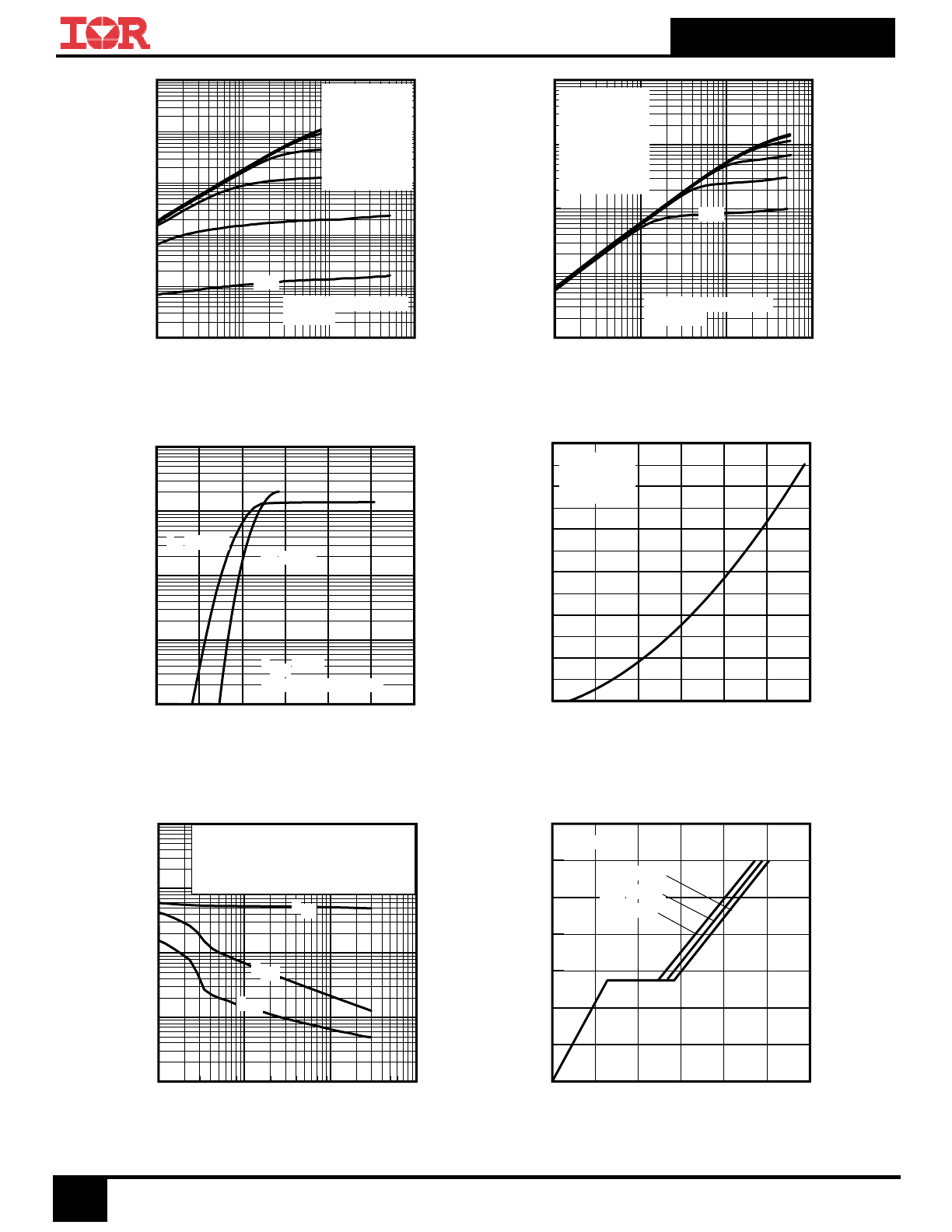
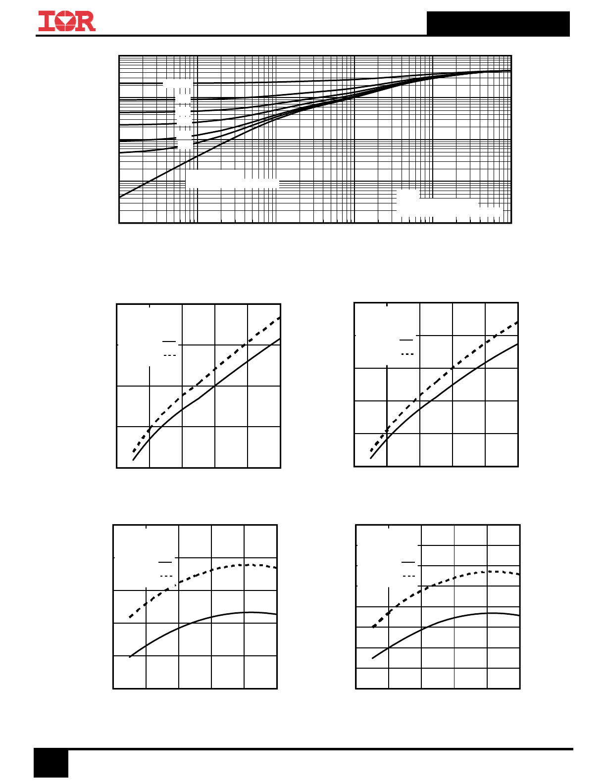
Fig 1. Typical Output Characteristics
2
4
6
8
10
12
14
VGS, Gate-to-Source Voltage (V)
0.1
1
10
100
1000
I D
, D
ra
in
-t
o-
S
ou
rc
e
C
ur
re
nt
(A
)
TJ = 25°C
TJ = 175°C
VDS = 50V
60µs PULSE WIDTH
Fig 4. Normalized On-Resistance vs. Temperature
Fig 5. Typical Capacitance vs. Drain-to-Source Voltage
Fig 6. Typical Gate Charge vs. Gate-to-Source Voltage
0.1
1
10
100
VDS, Drain-to-Source Voltage (V)
0.01
0.1
1
10
100
1000
I D
, D
ra
in
-t
o-
S
ou
rc
e
C
ur
re
nt
(
A
)
VGS
TOP 15V
10V
8.0V
7.0V
6.5V
6.0V
5.5V
BOTTOM
5.0V
60µs
PULSE WIDTH
Tj = 25°C
5.0V
0.1
1
10
100
VDS, Drain-to-Source Voltage (V)
0.1
1
10
100
1000
I D
, D
ra
in
-t
o
-S
ou
rc
e
C
ur
re
nt
(
A
)
5.0V
60µs
PULSE WIDTH
Tj = 175°C
VGS
TOP 15V
10V
8.0V
7.0V
6.5V
6.0V
5.5V
BOTTOM
5.0V
1
10
100
1000
VDS, Drain-to-Source Voltage (V)
10
100
1000
10000
100000
C
, C
ap
ac
ita
nc
e
(p
F
)
VGS = 0V, f = 1 MHZ
Ciss = Cgs + Cgd, Cds SHORTED
Crss = Cgd
Coss = Cds + Cgd
Coss
Crss
Ciss
Fig 3. Typical Transfer Characteristics
Fig 2. Typical Output Characteristics
-60
-20
20
60
100
140
180
TJ , Junction Temperature (°C)
0.5
1.0
1.5
2.0
2.5
3.0
3.5
R
D
S
(o
n)
,
D
ra
in
-t
o-
S
ou
rc
e
O
n
R
es
is
ta
nc
e
(
N
or
m
al
iz
ed
)
ID = 24A
VGS = 10V
0
20
40
60
80
100
120
QG, Total Gate Charge (nC)
0.0
2.0
4.0
6.0
8.0
10.0
12.0
14.0
V
G
S
, G
at
e-
to
-S
ou
rc
e
V
ol
ta
ge
(
V
)
VDS= 240V
VDS= 150V
VDS= 60V
ID = 24A
IRFB4137PbF
4
www.irf.com
© 2012 International Rectifier
October 30, 2012
-60
-20
20
60
100
140
180
TJ , Temperature ( °C )
270
280
290
300
310
320
330
340
350
360
370
V
(B
R
)D
S
S
,
D
ra
in
-t
o-
S
ou
rc
e
B
re
ak
do
w
n
V
ol
ta
ge
(
V
)
Id = 3.5mA
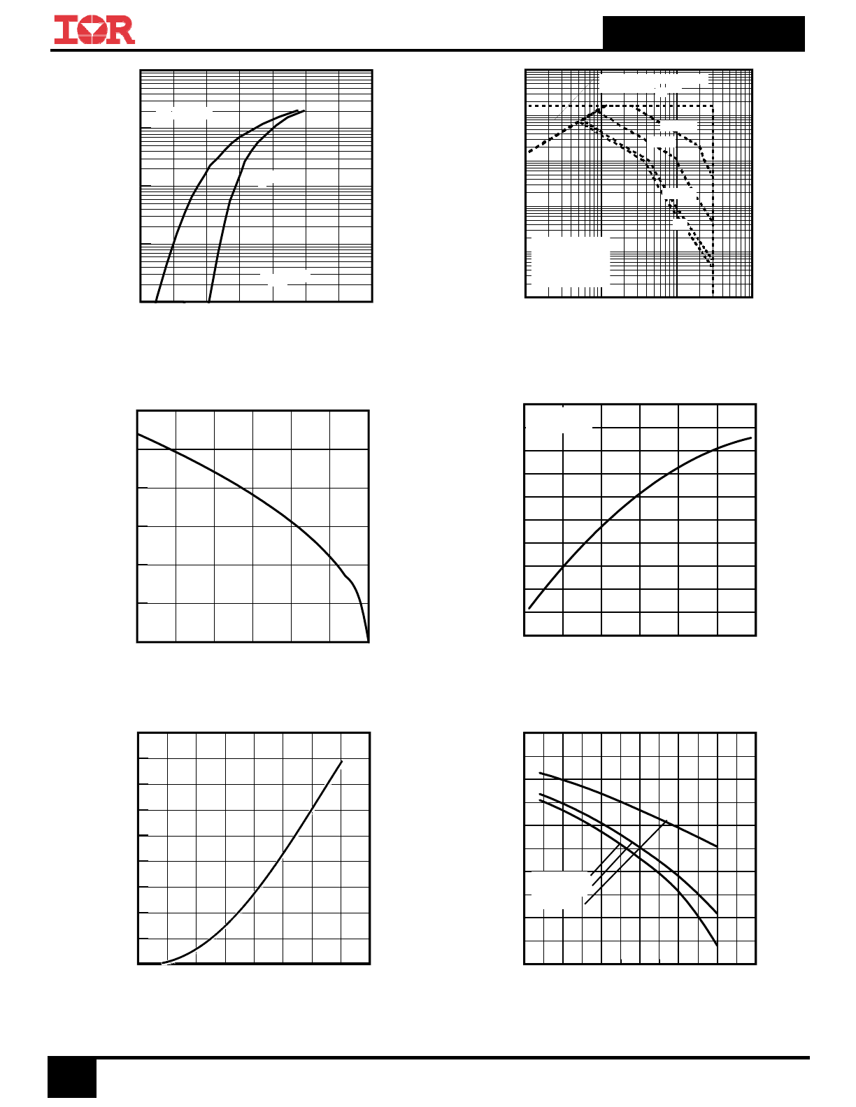
Fig 8. Maximum Safe Operating Area
-50
0
50
100 150 200 250 300 350
VDS, Drain-to-Source Voltage (V)
0.0
1.0
2.0
3.0
4.0
5.0
6.0
7.0
8.0
9.0
E
ne
rg
y
(µ
J)
Fig 11. Typical C
oss
Stored Energy
Fig 12. Threshold Voltage vs. Temperature
0.2
0.4
0.6
0.8
1.0
1.2
1.4
1.6
VSD, Source-to-Drain Voltage (V)
0.1
1
10
100
1000
I S
D
, R
ev
er
se
D
ra
in
C
ur
re
nt
(
A
)
TJ = 25°C
TJ = 175°C
VGS = 0V
Fig 7. Typical Source-Drain Diode Forward Voltage
-75
-25
25
75
125
175
225
TJ , Temperature ( °C )
1.0
2.0
3.0
4.0
5.0
6.0
V
G
S
(t
h)
,
G
at
e
th
re
sh
ol
d
V
ol
ta
ge
(
V
)
ID = 250µA
ID = 1.0mA
ID = 1.0A
Fig 10. Drain-to–Source Breakdown Voltage
1
10
100
1000
VDS, Drain-to-Source Voltage (V)
0.01
0.1
1
10
100
1000
I D
,
D
ra
in
-t
o-
S
ou
rc
e
C
ur
re
nt
(
A
)
Tc = 25°C
Tj = 175°C
Single Pulse
1msec
10msec
OPERATION IN THIS AREA
LIMITED BY R DS(on)
100µsec
DC
25
50
75
100
125
150
175
TC , Case Temperature (°C)
0
7
14
21
28
35
42
I D
,
D
ra
in
C
ur
re
nt
(
A
)
Fig 9. Maximum Drain Current vs. Case Temperature
IRFB4137PbF
5
www.irf.com
© 2012 International Rectifier
October 30, 2012
Fig 13. Maximum Effective Transient Thermal Impedance, Junction-to-Case
0
200
400
600
800
1000
diF /dt (A/µs)
1000
1500
2000
2500
3000
3500
Q
R
R
(
nC
)
IF = 16A
VR = 255V
TJ = 25°C
TJ = 125°C
0
200
400
600
800
1000
diF /dt (A/µs)
10
20
30
40
50
I R
R
M
(
A
)
IF = 16A
VR = 255V
TJ = 25°C
TJ = 125°C
Fig 16. Typical Stored Charge vs. dif/dt
Fig 17. Typical Stored Charge vs. dif/dt
Fig 14. Typical Recovery Current vs. dif/dt
0
200
400
600
800
1000
diF /dt (A/µs)
10
20
30
40
50
60
I R
R
M
(
A
)
IF = 24A
VR = 255V
TJ = 25°C
TJ = 125°C
0
200
400
600
800
1000
diF /dt (A/µs)
1000
1500
2000
2500
3000
3500
4000
4500
5000
Q
R
R
(
nC
)
IF = 24A
VR = 255V
TJ = 25°C
TJ = 125°C
Fig 15. Typical Recovery Current vs. dif/dt
1E-006
1E-005
0.0001
0.001
0.01
0.1
t1 , Rectangular Pulse Duration (sec)
0.0001
0.001
0.01
0.1
1
T
he
rma
l R
es
po
ns
e
(
Z
th
JC
)
°
C
/W
0.20
0.10
D = 0.50
0.02
0.01
0.05
SINGLE PULSE
( THERMAL RESPONSE )
Notes:
1. Duty Factor D = t1/t2
2. Peak Tj = P dm x Zthjc + Tc
IRFB4137PbF
6
www.irf.com
© 2012 International Rectifier
October 30, 2012
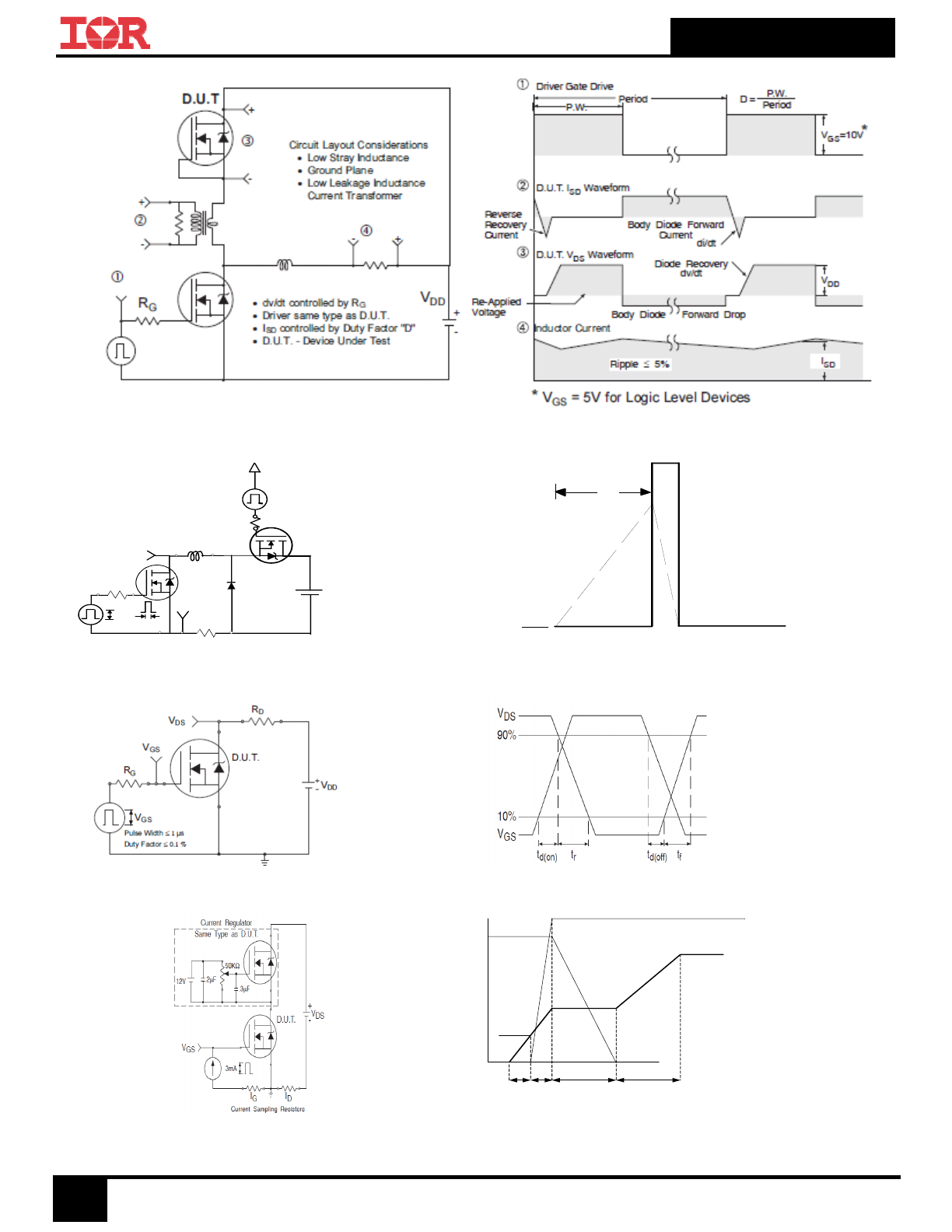
Fig 18. Peak Diode Recovery dv/dt Test Circuit for N-Channel HEXFET
®
Power MOSFETs
Fig 19a. Unclamped Inductive Test Circuit
R G
I
AS
0.01
tp
D.U.T
L
VDS
+
- VDD
DRIVER
A
15V
20V
Fig 20a. Switching Time Test Circuit
Fig 21a. Gate Charge Test Circuit
tp
V
(BR)DSS
I
AS
Fig 19b. Unclamped Inductive Waveforms
Fig 20b. Switching Time Waveforms
Vds
Vgs
Id
Vgs(th)
Qgs1 Qgs2
Qgd
Qgodr
Fig 21b. Gate Charge Waveform
IRFB4137PbF
7
www.irf.com
© 2012 International Rectifier
October 30, 2012
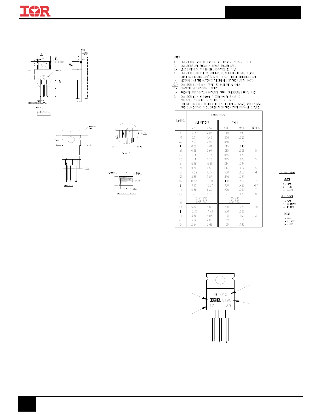
TO-220AB Package Outline (Dimensions are shown in millimeters (inches))
TO-220AB Part Marking Information
Note: For the most current drawing please refer to IR website at
http://www.irf.com/package/
IN T E R N A T IO N A L
P A R T N U M B E R
R E C T IF IE R
L O T C O D E
A S S E M B L Y
L O G O
Y E A R 0 = 2 0 0 0
D A T E C O D E
W E E K 1 9
L IN E C
L O T C O D E 1 7 8 9
E X A M P L E : T H IS IS A N IR F 1 0 1 0
N o t e : "P " in a s s e m b ly lin e p o s it io n
in d ic a t e s "L e a d - F r e e "
IN T H E A S S E M B L Y L IN E "C "
A S S E M B L E D O N W W 1 9 , 2 0 0 0
TO-220AB packages are not recommended for Surface Mount Application
.
IRFB4137PbF
8
www.irf.com
© 2012 International Rectifier
October 30, 2012
Qualification Information
†
Qualification Level
Industrial
(per JEDEC JESD47F)
††
Moisture Sensitivity Level
TO-220 N/A
RoHS Compliant
Yes
† Qualification standards can be found at International Rectifier’s web site
: http://www.irf.com/product-info/reliability/
†† Applicable version of JEDEC standard at the time of product release.
Data and specifications subject to change without notice.
IR WORLD HEADQUARTERS: 101N Sepulveda., El Segundo, California 90245, USA Tel: (310) 252-7105
TAC Fax: (310) 252-7903
Visit us at www.irf.com for sales contact information.