
HEXFET
®
Power MOSFET
Applications
l
High Efficiency Synchronous Rectification in SMPS
l
Uninterruptible Power Supply
l
High Speed Power Switching
l
Hard Switched and High Frequency Circuits
S
D
G
V
DSS
150V
R
DS(on)
typ.
9.3m
Ω
max.
11m
Ω
I
D
(Silicon Limited)
104A
Absolute Maximum Ratings
Symbol
Parameter
Units
I
D
@ T
C
= 25°C
Continuous Drain Current, V
GS
@ 10V
I
D
@ T
C
= 100°C
Continuous Drain Current, V
GS
@ 10V
I
DM
Pulsed Drain Current
c
P
D
@T
C
= 25°C
Maximum Power Dissipation
W
Linear Derating Factor
W/°C
V
GS
Gate-to-Source Voltage
V
dv/dt
Peak Diode Recovery
e
V/ns
T
J
Operating Junction and
T
STG
Storage Temperature Range
Soldering Temperature, for 10 seconds
(1.6mm from case)
Mounting torque, 6-32 or M3 screw
Avalanche Characteristics
E
AS (Thermally limited)
Single Pulse Avalanche Energy
d
mJ
Thermal Resistance
Symbol
Parameter
Typ.
Max.
Units
R
θJC
Junction-to-Case
j
–––
0.40
R
θCS
Case-to-Sink, Flat Greased Surface
0.50
–––
°C/W
R
θJA
Junction-to-Ambient
ij
–––
62
830
380
18
10lbxin (1.1Nxm)
A
°C
300
-55 to + 175
± 20
2.5
Max.
104
74
420
IRFB4115PbF
G
D
S
Gate
Drain
Source
TO-220AB
D
S
D
G
Benefits
l
Improved Gate, Avalanche and Dynamic dv/dt
Ruggedness
l
Fully Characterized Capacitance and Avalanche
SOA
l
Enhanced body diode dV/dt and dI/dt Capability
l
Lead Free
l
RoHS Compliant, Halogen-Free
1
www.irf.com
©
2014 International Rectifier
Submit Datasheet Feedback
November 11, 2014
Form
Quantity
IRFB4115PbF
TO-220
Tube
50
IRFB4115PbF
Base Part Number
Package Type
Standard Pack
Orderable Part Number
IRFB4115PbF
2
www.irf.com
©
2014 International Rectifier
Submit Datasheet Feedback
November 11, 2014
Notes:
Repetitive rating; pulse width limited by max. junction
temperature.
Recommended max EAS limit, starting T
J
= 25°C,
L = 0.17mH, R
G
= 25
Ω, I
AS
= 100A, V
GS
=15V.
I
SD
≤ 62A, di/dt ≤ 1040A/µs, V
DD
≤ V
(BR)DSS
, T
J
≤ 175°C.
Pulse width
≤ 400µs; duty cycle ≤ 2%.
S
D
G
C
oss
eff. (TR) is a fixed capacitance that gives the same charging time
as C
oss
while V
DS
is rising from 0 to 80% V
DSS
.
C
oss
eff. (ER) is a fixed capacitance that gives the same energy as
C
oss
while V
DS
is rising from 0 to 80% V
DSS
.
When mounted on 1" square PCB (FR-4 or G-10 Material). For recom
mended footprint and soldering techniques refer to application note #AN-994.
R
θ
is measured at T
J
approximately 90°C.
Static @ T
J
= 25°C (unless otherwise specified)
Symbol
Parameter
Min. Typ. Max. Units
V
(BR)DSS
Drain-to-Source Breakdown Voltage
150
–––
–––
V
∆V
(BR)DSS
/
∆T
J
Breakdown Voltage Temp. Coefficient
–––
0.18
–––
V/°C
R
DS(on)
Static Drain-to-Source On-Resistance
–––
9.3
11
m
Ω
V
GS(th)
Gate Threshold Voltage
3.0
–––
5.0
V
I
DSS
Drain-to-Source Leakage Current
–––
–––
20
µA
–––
–––
250
I
GSS
Gate-to-Source Forward Leakage
–––
–––
100
nA
Gate-to-Source Reverse Leakage
–––
–––
-100
R
G
Internal Gate Resistance
–––
2.3
–––
Ω
Dynamic @ T
J
= 25°C (unless otherwise specified)
Symbol
Parameter
Min. Typ. Max. Units
gfs
Forward Transconductance
97
–––
–––
S
Q
g
Total Gate Charge
–––
77
120
nC
Q
gs
Gate-to-Source Charge
–––
28
–––
Q
gd
Gate-to-Drain ("Miller") Charge
–––
26
–––
Q
sync
Total Gate Charge Sync. (Q
g
- Q
gd
)
–––
51
–––
t
d(on)
Turn-On Delay Time
–––
18
–––
ns
t
r
Rise Time
–––
73
–––
t
d(off)
Turn-Off Delay Time
–––
41
–––
t
f
Fall Time
–––
39
–––
C
iss
Input Capacitance
–––
5270
–––
pF
C
oss
Output Capacitance
–––
490
–––
C
rss
Reverse Transfer Capacitance
–––
105
–––
C
oss
eff. (ER) Effective Output Capacitance (Energy Related) –––
460
–––
C
oss
eff. (TR) Effective Output Capacitance (Time Related)
–––
530
–––
Diode Characteristics
Symbol
Parameter
Min. Typ. Max. Units
I
S
Continuous Source Current
–––
–––
104
A
(Body Diode)
I
SM
Pulsed Source Current
–––
–––
420
A
(Body Diode)
d
V
SD
Diode Forward Voltage
–––
–––
1.3
V
t
rr
Reverse Recovery Time
–––
86
–––
ns
T
J
= 25°C
V
R
= 130V,
–––
110
–––
T
J
= 125°C
I
F
= 62A
Q
rr
Reverse Recovery Charge
–––
300
–––
nC T
J
= 25°C
di/dt = 100A/µs
f
–––
450
–––
T
J
= 125°C
I
RRM
Reverse Recovery Current
–––
6.5
–––
A
T
J
= 25°C
t
on
Forward Turn-On Time
Intrinsic turn-on time is negligible (turn-on is dominated by LS+LD)
I
D
= 62A
R
G
= 2.2
Ω
V
GS
= 10V
f
V
DD
= 98V
I
D
= 62A, V
DS
=0V, V
GS
= 10V
T
J
= 25°C, I
S
= 62A, V
GS
= 0V
f
integral reverse
p-n junction diode.
Conditions
V
GS
= 0V, I
D
= 250µA
Reference to 25°C, I
D
= 3.5mA
c
V
GS
= 10V, I
D
= 62A
f
V
DS
= V
GS
, I
D
= 250µA
V
DS
= 150V, V
GS
= 0V
V
DS
= 150V, V
GS
= 0V, T
J
= 125°C
MOSFET symbol
showing the
V
DS
= 75V
Conditions
V
GS
= 10V
f
V
GS
= 0V
V
DS
= 50V
ƒ = 1.0 MHz, See Fig. 5
V
GS
= 0V, V
DS
= 0V to 120V
h, See Fig. 11
V
GS
= 0V, V
DS
= 0V to 120V
g
Conditions
V
DS
= 50V, I
D
= 62A
I
D
= 62A
V
GS
= 20V
V
GS
= -20V
IRFB4115PbF
3
www.irf.com
©
2014 International Rectifier
Submit Datasheet Feedback
November 11, 2014
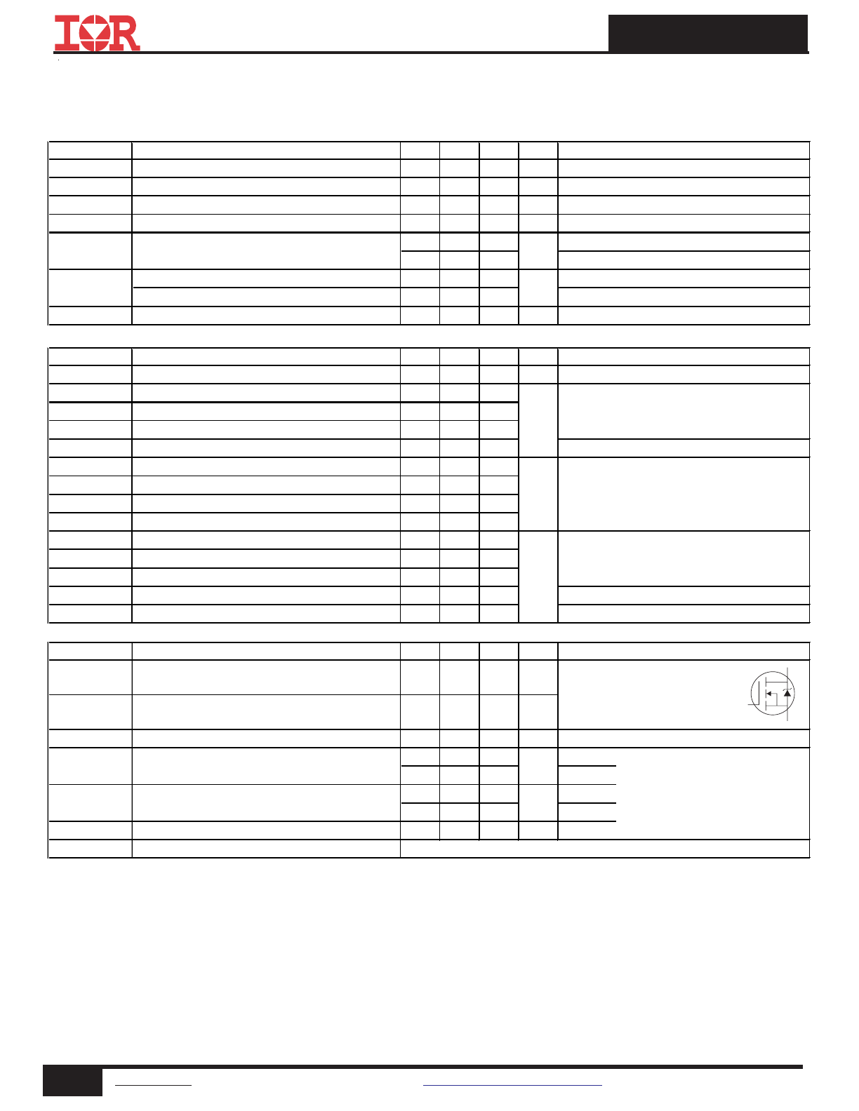
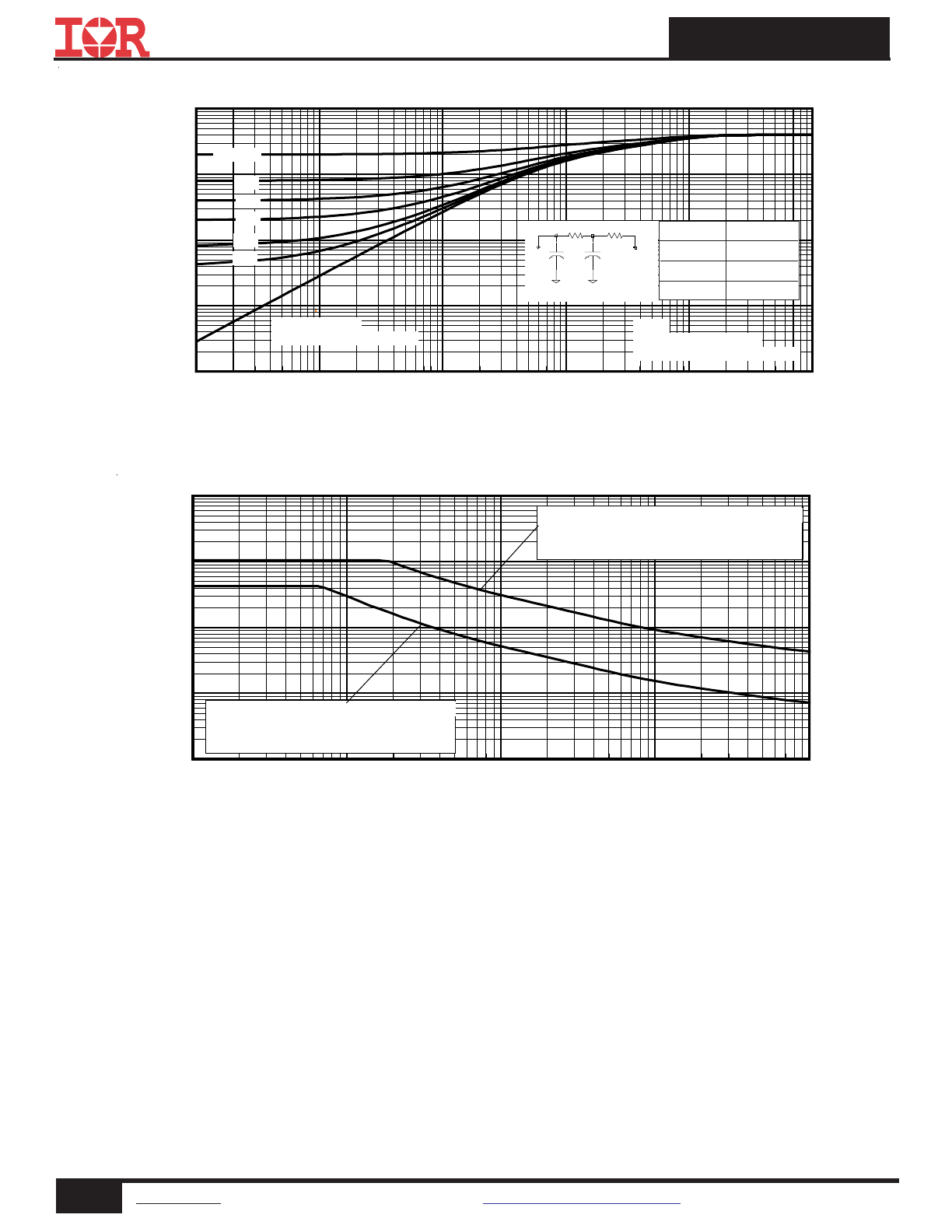
Fig 1. Typical Output Characteristics
Fig 3. Typical Transfer Characteristics
Fig 4. Normalized On-Resistance vs. Temperature
Fig 2. Typical Output Characteristics
Fig 6. Typical Gate Charge vs. Gate-to-Source Voltage
Fig 5. Typical Capacitance vs. Drain-to-Source Voltage
0.1
1
10
100
VDS, Drain-to-Source Voltage (V)
0.1
1
10
100
1000
I D
, D
ra
in
-t
o-
S
ou
rc
e
C
ur
re
nt
(
A
)
VGS
TOP
15V
10V
8.0V
7.0V
6.5V
6.0V
5.5V
BOTTOM
5.0V
≤60µs PULSE WIDTH
Tj = 25°C
5.0V
1
10
100
1000
VDS, Drain-to-Source Voltage (V)
10
100
1000
10000
100000
C
, C
ap
ac
ita
nc
e
(p
F
)
VGS = 0V, f = 1 MHZ
Ciss = Cgs + Cgd, C ds SHORTED
Crss = Cgd
Coss = Cds + Cgd
Coss
Crss
Ciss
2
4
6
8
10
12
14
16
VGS, Gate-to-Source Voltage (V)
0.1
1
10
100
1000
I D
, D
ra
in
-t
o-
S
ou
rc
e
C
ur
re
nt
(
A
)
TJ = 25°C
TJ = 175°C
VDS = 50V
≤60µs PULSE WIDTH
0
20
40
60
80
100
QG, Total Gate Charge (nC)
0.0
2.0
4.0
6.0
8.0
10.0
12.0
14.0
V
G
S
, G
at
e-
to
-S
ou
rc
e
V
ol
ta
ge
(
V
)
VDS= 120V
VDS= 75V
VDS= 30V
ID= 62A
0.1
1
10
100
VDS, Drain-to-Source Voltage (V)
1
10
100
1000
I D
, D
ra
in
-t
o-
S
ou
rc
e
C
ur
re
nt
(
A
)
5.0V
≤60µs PULSE WIDTH
Tj = 175°C
VGS
TOP
15V
10V
8.0V
7.0V
6.5V
6.0V
5.5V
BOTTOM
5.0V
-60 -40 -20 0 20 40 60 80 100120140160180
TJ , Junction Temperature (°C)
0.5
1.0
1.5
2.0
2.5
3.0
R
D
S
(o
n)
,
D
ra
in
-t
o-
S
ou
rc
e
O
n
R
es
is
ta
nc
e
(
N
or
m
al
iz
ed
)
ID = 62A
VGS = 10V
IRFB4115PbF
4
www.irf.com
©
2014 International Rectifier
Submit Datasheet Feedback
November 11, 2014
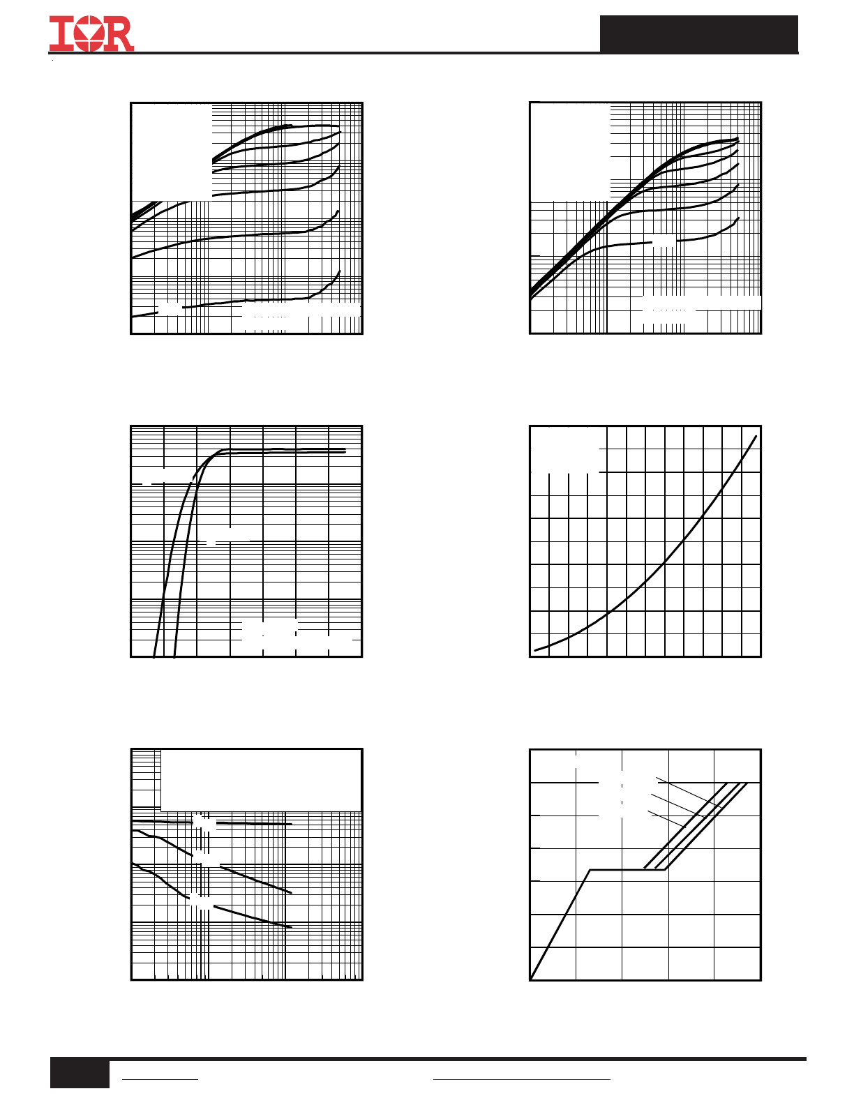
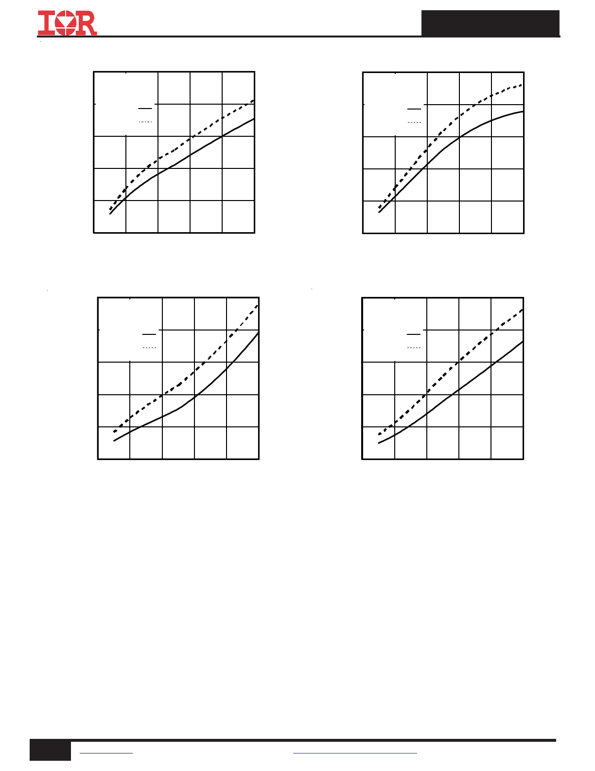
Fig 8. Maximum Safe Operating Area
Fig 10. Drain-to-Source Breakdown Voltage
Fig 7. Typical Source-Drain Diode
Forward Voltage
Fig 11. Typical C
OSS
Stored Energy
Fig 9. Maximum Drain Current vs.
Case Temperature
0.0
0.5
1.0
1.5
2.0
2.5
3.0
3.5
VSD, Source-to-Drain Voltage (V)
0.1
1
10
100
1000
I S
D
, R
ev
er
se
D
ra
in
C
ur
re
nt
(
A
)
TJ = 25°C
TJ = 175°C
VGS = 0V
25
50
75
100
125
150
175
TC , Case Temperature (°C)
0
20
40
60
80
100
120
I D
,
D
ra
in
C
ur
re
nt
(
A
)
-60 -40 -20 0 20 40 60 80 100120140160180
TJ , Temperature ( °C )
140
150
160
170
180
190
200
V
(B
R
)D
S
S
, D
ra
in
-t
o-
S
ou
rc
e
B
re
ak
do
w
n
V
ol
ta
ge
(
V
)
Id = 3.5mA
-20
0
20
40
60
80 100 120 140 160
VDS, Drain-to-Source Voltage (V)
0.0
1.0
2.0
3.0
4.0
5.0
6.0
E
ne
rg
y
(µ
J)
1
10
100
1000
VDS, Drain-to-Source Voltage (V)
1
10
100
1000
10000
I D
,
D
ra
in
-t
o-
S
ou
rc
e
C
ur
re
nt
(
A
)
OPERATION IN THIS AREA
LIMITED BY R DS(on)
Tc = 25°C
Tj = 175°C
Single Pulse
100µsec
1msec
10msec
DC
Fig 12. Threshold Voltage vs. Temperature
-75 -50 -25 0
25 50 75 100 125 150 175
TJ , Temperature ( °C )
1.0
2.0
3.0
4.0
5.0
6.0
V
G
S
(t
h)
, G
at
e
th
re
sh
ol
d
V
ol
ta
ge
(
V
)
ID = 250µA
ID = 1.0mA
ID = 1.0A
IRFB4115PbF
5
www.irf.com
©
2014 International Rectifier
Submit Datasheet Feedback
November 11, 2014
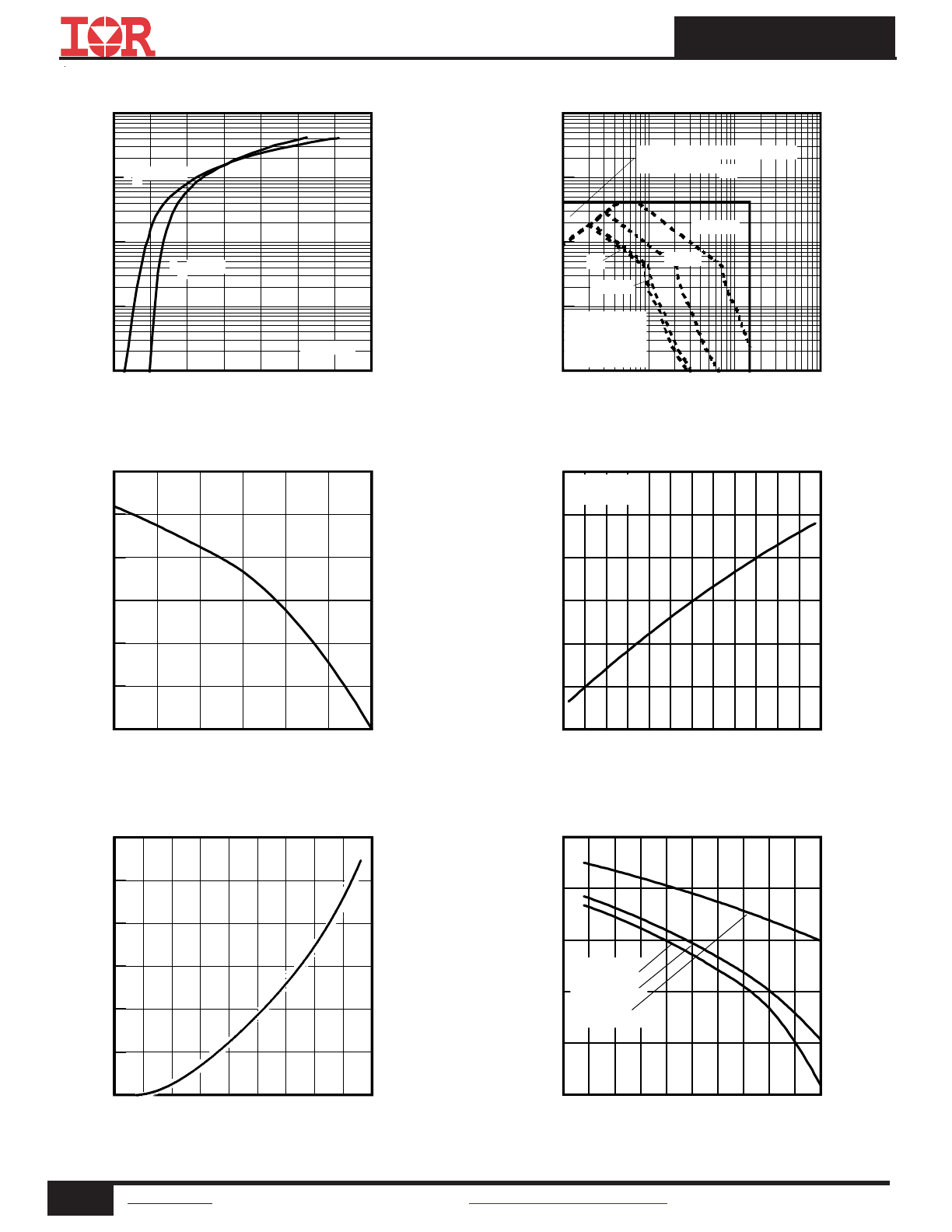
Fig 13. Maximum Effective Transient Thermal Impedance, Junction-to-Case
1E-006
1E-005
0.0001
0.001
0.01
0.1
t1 , Rectangular Pulse Duration (sec)
0.0001
0.001
0.01
0.1
1
T
he
rm
al
R
es
po
ns
e
(
Z
th
JC
)
°
C
/W
0.20
0.10
D = 0.50
0.02
0.01
0.05
SINGLE PULSE
( THERMAL RESPONSE )
Notes:
1. Duty Factor D = t1/t2
2. Peak Tj = P dm x Zthjc + Tc
Ri (°C/W)
τi (sec)
0.245 0.0059149
0.155 0.0006322
τ
J
τ
J
τ
1
τ
1
τ
2
τ
2
R
1
R
1
R
2
R
2
τ
C
τ
C
Ci=
τi/Ri
Ci=
τi/Ri
Fig 14. Typical Avalanche Current vs.Pulsewidth
1.0E-06
1.0E-05
1.0E-04
1.0E-03
1.0E-02
tav (sec)
0.1
1
10
100
1000
A
va
la
nc
he
C
ur
re
nt
(
A
)
Allowed avalanche Current vs avalanche
pulsewidth, tav, assuming
∆Τ j = 25°C and
Tstart = 150°C.
Allowed avalanche Current vs avalanche
pulsewidth, tav, assuming
∆Tj = 150°C and
Tstart = 25°C (Single Pulse)
IRFB4115PbF
6
www.irf.com
©
2014 International Rectifier
Submit Datasheet Feedback
November 11, 2014
Fig 15. - Typical Recovery Current vs. di
f
/dt
0
200
400
600
800
1000
diF /dt (A/µs)
0
10
20
30
40
50
I R
R
(
A
)
IF = 42A
VR = 130V
TJ = 25°C
TJ = 125°C
Fig 16. - Typical Recovery Current vs. di
f
/dt
0
200
400
600
800
1000
diF /dt (A/µs)
0
10
20
30
40
50
I R
R
(
A
)
IF = 62A
VR = 130V
TJ = 25°C
TJ = 125°C
Fig 18. - Typical Stored Charge vs. di
f
/dt
Fig 17. - Typical Stored Charge vs. di
f
/dt
0
200
400
600
800
1000
diF /dt (A/µs)
0
500
1000
1500
2000
2500
Q
R
R
(
nC
)
IF = 42A
VR = 130V
TJ = 25°C
TJ = 125°C
0
200
400
600
800
1000
diF /dt (A/µs)
0
600
1200
1800
2400
3000
Q
R
R
(
nC
)
IF = 62A
VR = 130V
TJ = 25°C
TJ = 125°C
IRFB4115PbF
7
www.irf.com
©
2014 International Rectifier
Submit Datasheet Feedback
November 11, 2014
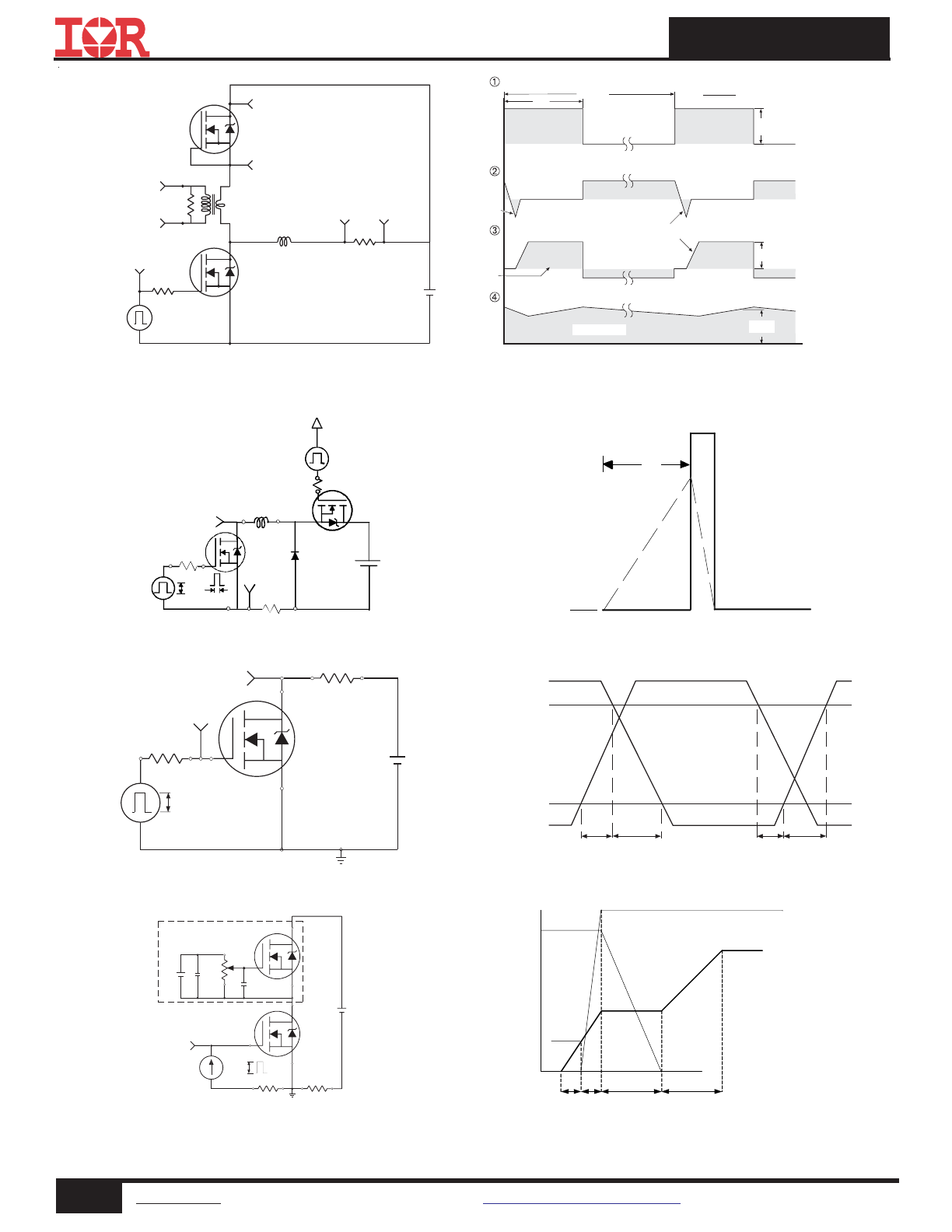
Fig 21a. Switching Time Test Circuit
Fig 21b. Switching Time Waveforms
Fig 20b. Unclamped Inductive Waveforms
Fig 20a. Unclamped Inductive Test Circuit
tp
V
(BR)DSS
I
AS
RG
IAS
0.01
Ω
tp
D.U.T
L
VDS
+
- VDD
DRIVER
A
15V
20V
V
GS
Fig 22a. Gate Charge Test Circuit
Fig 22b. Gate Charge Waveform
Vds
Vgs
Id
Vgs(th)
Qgs1 Qgs2
Qgd
Qgodr
Fig 19.
Peak Diode Recovery dv/dt Test Circuit for N-Channel
HEXFET
®
Power MOSFETs
Circuit Layout Considerations
• Low Stray Inductance
• Ground Plane
• Low Leakage Inductance
Current Transformer
P.W.
Period
di/dt
Diode Recovery
dv/dt
Ripple
≤ 5%
Body Diode Forward Drop
Re-Applied
Voltage
Reverse
Recovery
Current
Body Diode Forward
Current
V
GS
=10V
V
DD
I
SD
Driver Gate Drive
D.U.T. I
SD
Waveform
D.U.T. V
DS
Waveform
Inductor Curent
D =
P.W.
Period
*
V
GS
= 5V for Logic Level Devices
*
+
-
+
+
+
-
-
-
R
G
V
DD
• dv/dt controlled by R
G
• Driver same type as D.U.T.
• I
SD
controlled by Duty Factor "D"
• D.U.T. - Device Under Test
D.U.T
Inductor Current
D.U.T.
V
DS
I
D
I
G
3mA
V
GS
.3
µF
50K
Ω
.2
µF
12V
Current Regulator
Same Type as D.U.T.
Current Sampling Resistors
+
-
V
DS
90%
10%
V
GS
t
d(on)
t
r
t
d(off)
t
f
V
DS
Pulse Width ≤ 1 µs
Duty Factor ≤ 0.1 %
R
D
V
GS
R
G
D.U.T.
10V
+
-
V
DD
V
GS
IRFB4115PbF
8
www.irf.com
©
2014 International Rectifier
Submit Datasheet Feedback
November 11, 2014
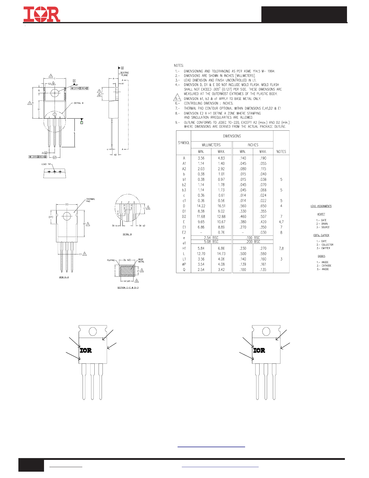
TO-220AB Package Outline
Dimensions are shown in millimeters (inches)
TO-220AB Part Marking Information
TO-220AB packages are not recommended for Surface Mount Application.
Note: For the most current drawing please refer to IR website at:
http://www.irf.com/package/
IRFB4115
IRFB4115
g
PYWW?
LC LC
PART NUMBER
DATE CODE
P = LEAD-FREE
Y = LAST DIGIT OF YEAR
WW = WORK WEEK
? = ASSEMBLY SITE CODE
INTERNATIONAL
RECTIFIER LOGO
ASSEMBLY
LOT CODE
OR
YWWP
LC LC
PART NUMBER
DATE CODE
Y = LAST DIGIT OF YEAR
WW = WORK WEEK
P = LEAD-FREE
INTERNATIONAL
RECTIFIER LOGO
ASSEMBLY
LOT CODE
IRFB4115PbF
9
www.irf.com
©
2014 International Rectifier
Submit Datasheet Feedback
November 11, 2014
Qualification standards can be found at International Rectifiers web site:
http://www.irf.com/product-info/reliability/
Applicable version of JEDEC standard at the time of product release.
Moisture Sensitivity Level
TO-220
N/A
RoHS compliant
Qualification information
†
Industrial
†
(per JEDEC JESD47F
††
guidelines)
Yes
Qualification level
IR WORLD HEADQUARTERS: 101 N. Sepulveda Blvd., El Segundo, California 90245, USA
To contact International Rectifier, please visit
http://www.irf.com/whoto-call/
Revision History
Date
Comment
• Updated data sheet with new IR corporate template.
• Updated package outline & part marking on page 7.
• Added bullet point in the Benefits "RoHS Compliant, Halogen -Free" on page 1.
• Updated typo on the Fig.16 and Fig.17, unit of Y-axis from "A" to "nC" on page 5.
11/6/2014
• Added Fig 14 - Typical Avalanc
he Current vs Pulsewidth on page 5.
4/28/2014