
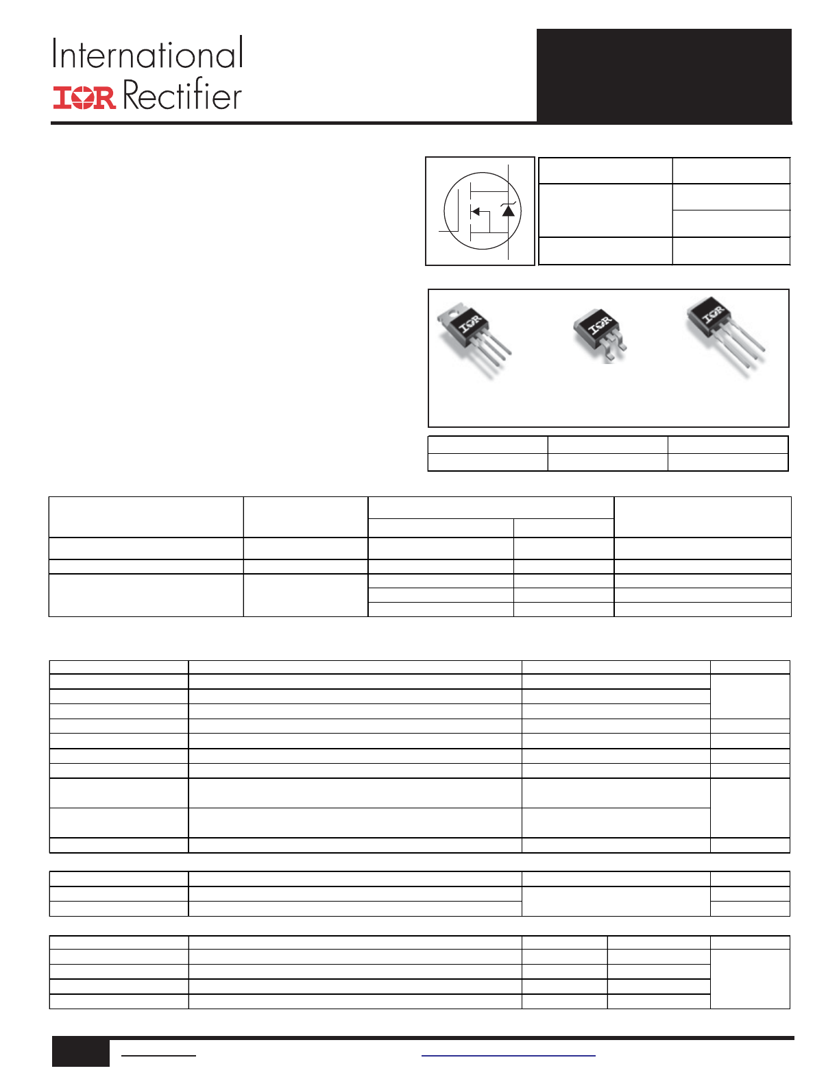
HEXFET
®
Power MOSFET
S
D
G
Benefits
l
Improved Gate, Avalanche and Dynamic dV/dt
Ruggedness
l
Fully Characterized Capacitance and Avalanche
SOA
l
Enhanced body diode dV/dt and dI/dt Capability
l
Lead-Free
l
RoHS Compliant, Halogen-Free
Applications
l
High Efficiency Synchronous Rectification in SMPS
l
Uninterruptible Power Supply
l
High Speed Power Switching
l
Hard Switched and High Frequency Circuits
D
2
Pak
IRFS4410ZPbF
TO-220AB
IRFB4410ZPbF
TO-262
IRFSL4410ZPbF
S
D
G
S
D
G
S
D
G
D
D
D
G
D
S
Gate
Drain
Source
V
DSS
100V
R
DS(on)
typ.
7.2m
:
max.
9.0m
:
I
D (Silicon Limited)
97A
IRFB4410ZPbF
IRFS4410ZPbF
IRFSL4410ZPbF
Form
Quantity
IRFB4410ZPbF
TO-220
Tube
50
IRFB4410ZPbF
IRFSL4410ZPbF
TO-262
Tube
50
IRFSL4410ZPbF
Tube
50
IRFS4410ZPbF
Tape and Reel Left
800
IRFS4410ZTRLPbF
Tape and Reel Right
800
IRFS4410ZTRRPbF
Base Part Number
Package Type
Standard Pack
Orderable Part Number
IRFS4410ZPbF
D2Pak
1
www.irf.com
©
2014 International Rectifier
Submit Datasheet Feedback
April 25, 2014
Absolute Maximum Ratings
Symbol
Parameter
Units
I
D
@ T
C
= 25°C
Continuous Drain Current, V
GS
@ 10V (Silicon Limited)
I
D
@ T
C
= 100°C
Continuous Drain Current, VGS @ 10V (Silicon Limited)
A
I
DM
Pulsed Drain Current c
P
D
@T
C
= 25°C
Maximum Power Dissipation
W
Linear Derating Factor
W/°C
V
GS
Gate-to-Source Voltage
V
dv/dt
Peak Diode Recovery e
V/ns
T
J
Operating Junction and
°C
T
STG
Storage Temperature Range
Soldering Temperature, for 10 seconds
(1.6mm from case)
Mounting torque, 6-32 or M3 screw
Avalanche Characteristics
E
AS (Thermally limited)
Single Pulse Avalanche Energy d
mJ
I
AR
Avalanche Current
A
E
AR
Repetitive Avalanche Energy f
mJ
Thermal Resistance
Symbol
Parameter
Typ.
Max.
Units
R
θJC
Junction-to-Case j
–––
0.65
R
θCS
Case-to-Sink, Flat Greased Surface , TO-220
0.50
–––
°C/W
R
θJA
Junction-to-Ambient, TO-220 j
–––
62
R
θJA
Junction-to-Ambient (PCB Mount) , D
2
Pak ij
–––
40
300
Max.
97
69
390
242
See Fig. 14, 15, 22a, 22b,
230
16
-55 to + 175
± 20
1.5
10lbx in (1.1Nx m)
2
www.irf.com
©
2014 International Rectifier
Submit Datasheet Feedback
April 25, 2014
IRFB4410ZPbF/IRFS4410ZPbF/IRFSL4410ZPbF
Notes:
Repetitive rating; pulse width limited by max. junction
temperature.
Limited by T
Jmax
, starting T
J
= 25°C, L = 0.143mH
R
G
= 25
Ω, I
AS
= 58A, V
GS
=10V. Part not recommended for use
above this value.
I
SD
≤ 58A, di/dt ≤ 610A/μs, V
DD
≤ V
(BR)DSS
, T
J
≤ 175°C.
Pulse width ≤ 400μs; duty cycle ≤ 2%.
S
D
G
C
oss
eff. (TR) is a fixed capacitance that gives the same charging time
as C
oss
while V
DS
is rising from 0 to 80% V
DSS
.
C
oss
eff. (ER) is a fixed capacitance that gives the same energy as
C
oss
while V
DS
is rising from 0 to 80% V
DSS
.
When mounted on 1" square PCB (FR-4 or G-10 Material). For recom
mended footprint and soldering techniques refer to application note #AN-994.
R
θ
is measured at T
J
approximately 90°C.
Static @ T
J
= 25°C (unless otherwise specified)
Symbol
Parameter
Min. Typ. Max. Units
V
(BR)DSS
Drain-to-Source Breakdown Voltage
100
–––
–––
V
ΔV
(BR)DSS
/
ΔT
J
Breakdown Voltage Temp. Coefficient
–––
0.12
–––
V/°C
R
DS(on)
Static Drain-to-Source On-Resistance
–––
7.2
9.0
m
Ω
V
GS(th)
Gate Threshold Voltage
2.0
–––
4.0
V
I
DSS
Drain-to-Source Leakage Current
–––
–––
20
μA
–––
–––
250
I
GSS
Gate-to-Source Forward Leakage
–––
–––
100
nA
Gate-to-Source Reverse Leakage
–––
–––
-100
R
G
Internal Gate Resistance
–––
0.70
–––
Ω
Dynamic @ T
J
= 25°C (unless otherwise specified)
Symbol
Parameter
Min. Typ. Max. Units
gfs
Forward Transconductance
140
–––
–––
S
Q
g
Total Gate Charge
–––
83
120
nC
Q
gs
Gate-to-Source Charge
–––
19
–––
Q
gd
Gate-to-Drain ("Miller") Charge
–––
27
Q
sync
Total Gate Charge Sync. (Q
g
- Q
gd
)
–––
56
–––
t
d(on)
Turn-On Delay Time
–––
16
–––
ns
t
r
Rise Time
–––
52
–––
t
d(off)
Turn-Off Delay Time
–––
43
–––
t
f
Fall Time
–––
57
–––
C
iss
Input Capacitance
–––
4820
–––
pF
C
oss
Output Capacitance
–––
340
–––
C
rss
Reverse Transfer Capacitance
–––
170
–––
C
oss
eff. (ER) Effective Output Capacitance (Energy Related) h––– 420 –––
C
oss
eff. (TR) Effective Output Capacitance (Time Related)g
–––
690
–––
Diode Characteristics
Symbol
Parameter
Min. Typ. Max. Units
I
S
Continuous Source Current
–––
–––
97
A
(Body Diode)
I
SM
Pulsed Source Current
–––
–––
390
A
(Body Diode)
c
V
SD
Diode Forward Voltage
–––
–––
1.3
V
t
rr
Reverse Recovery Time
–––
38
57
ns
T
J
= 25°C
V
R
= 85V,
–––
46
69
T
J
= 125°C
I
F
= 58A
Q
rr
Reverse Recovery Charge
–––
53
80
nC T
J
= 25°C
di/dt = 100A/μs
f
–––
82
120
T
J
= 125°C
I
RRM
Reverse Recovery Current
–––
2.5
–––
A
T
J
= 25°C
t
on
Forward Turn-On Time
Intrinsic turn-on time is negligible (turn-on is dominated by LS+LD)
I
D
= 58A
R
G
=2.7
Ω
V
GS
= 10V
f
V
DD
= 65V
I
D
= 58A, V
DS
=0V, V
GS
= 10V
f
T
J
= 25°C, I
S
= 58A, V
GS
= 0V
f
integral reverse
p-n junction diode.
Conditions
V
GS
= 0V, I
D
= 250μA
Reference to 25°C, I
D
= 5mAc
V
GS
= 10V, I
D
= 58A f
V
DS
= V
GS
, I
D
= 150μA
V
DS
= 100V, V
GS
= 0V
V
DS
= 80V, V
GS
= 0V, T
J
= 125°C
MOSFET symbol
showing the
V
DS
=50V
Conditions
V
GS
= 10V
f
V
GS
= 0V
V
DS
= 50V
ƒ = 1.0MHz, See Fig.5
V
GS
= 0V, V
DS
= 0V to 80V
h, See Fig.11
V
GS
= 0V, V
DS
= 0V to 80V
g
Conditions
V
DS
= 10V, I
D
= 58A
I
D
= 58A
V
GS
= 20V
V
GS
= -20V
3
www.irf.com
©
2014 International Rectifier
Submit Datasheet Feedback
April 25, 2014
IRFB4410ZPbF/IRFS4410ZPbF/IRFSL4410ZPbF
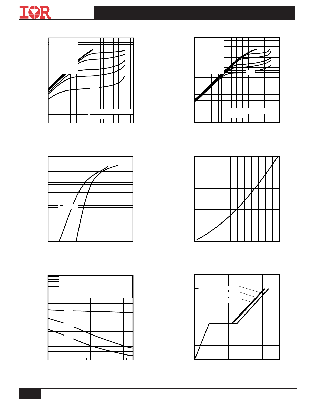
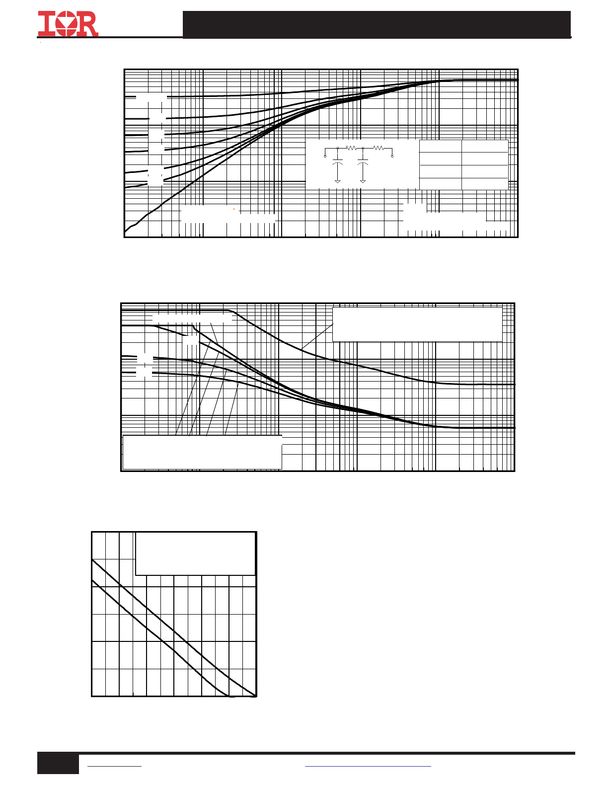
Fig 1. Typical Output Characteristics
Fig 3. Typical Transfer Characteristics
Fig 4. Normalized On-Resistance vs. Temperature
Fig 2. Typical Output Characteristics
Fig 6. Typical Gate Charge vs. Gate-to-Source Voltage
Fig 5. Typical Capacitance vs. Drain-to-Source Voltage
0.1
1
10
100
VDS, Drain-to-Source Voltage (V)
1
10
100
1000
I D
, D
ra
in
-t
o-
S
ou
rc
e
C
ur
re
nt
(
A
)
VGS
TOP
15V
10V
8.0V
6.0V
5.5V
5.0V
4.8V
BOTTOM
4.5V
≤60μs PULSE WIDTH
Tj = 25°C
4.5V
0.1
1
10
100
VDS, Drain-to-Source Voltage (V)
1
10
100
1000
I D
, D
ra
in
-t
o-
S
ou
rc
e
C
ur
re
nt
(
A
)
4.5V
≤60μs PULSE WIDTH
Tj = 175°C
VGS
TOP
15V
10V
8.0V
6.0V
5.5V
5.0V
4.8V
BOTTOM
4.5V
0
20
40
60
80
100
QG, Total Gate Charge (nC)
0.0
2.0
4.0
6.0
8.0
10.0
12.0
V
G
S
, G
at
e-
to
-S
ou
rc
e
V
ol
ta
ge
(
V
)
VDS= 80V
VDS= 40V
VDS= 20V
ID= 58A
2
3
4
5
6
7
VGS, Gate-to-Source Voltage (V)
0.1
1
10
100
1000
I D
, D
ra
in
-t
o-
S
ou
rc
e
C
ur
re
nt
(
A
)
TJ = 25°C
TJ = 175°C
VDS = 50V
≤60μs PULSE WIDTH
-60 -40 -20 0 20 40 60 80 100120140160180
TJ , Junction Temperature (°C)
0.5
1.0
1.5
2.0
2.5
R
D
S
(o
n)
,
D
ra
in
-t
o-
S
ou
rc
e
O
n
R
es
is
ta
nc
e
(
N
or
m
al
iz
ed
)
ID = 58A
VGS = 10V
1
10
100
VDS, Drain-to-Source Voltage (V)
100
1000
10000
100000
C
, C
ap
ac
ita
nc
e
(p
F
)
VGS = 0V, f = 1 MHZ
Ciss = Cgs + Cgd, C ds SHORTED
Crss = Cgd
Coss = Cds + Cgd
Coss
Crss
Ciss
4
www.irf.com
©
2014 International Rectifier
Submit Datasheet Feedback
April 25, 2014
IRFB4410ZPbF/IRFS4410ZPbF/IRFSL4410ZPbF
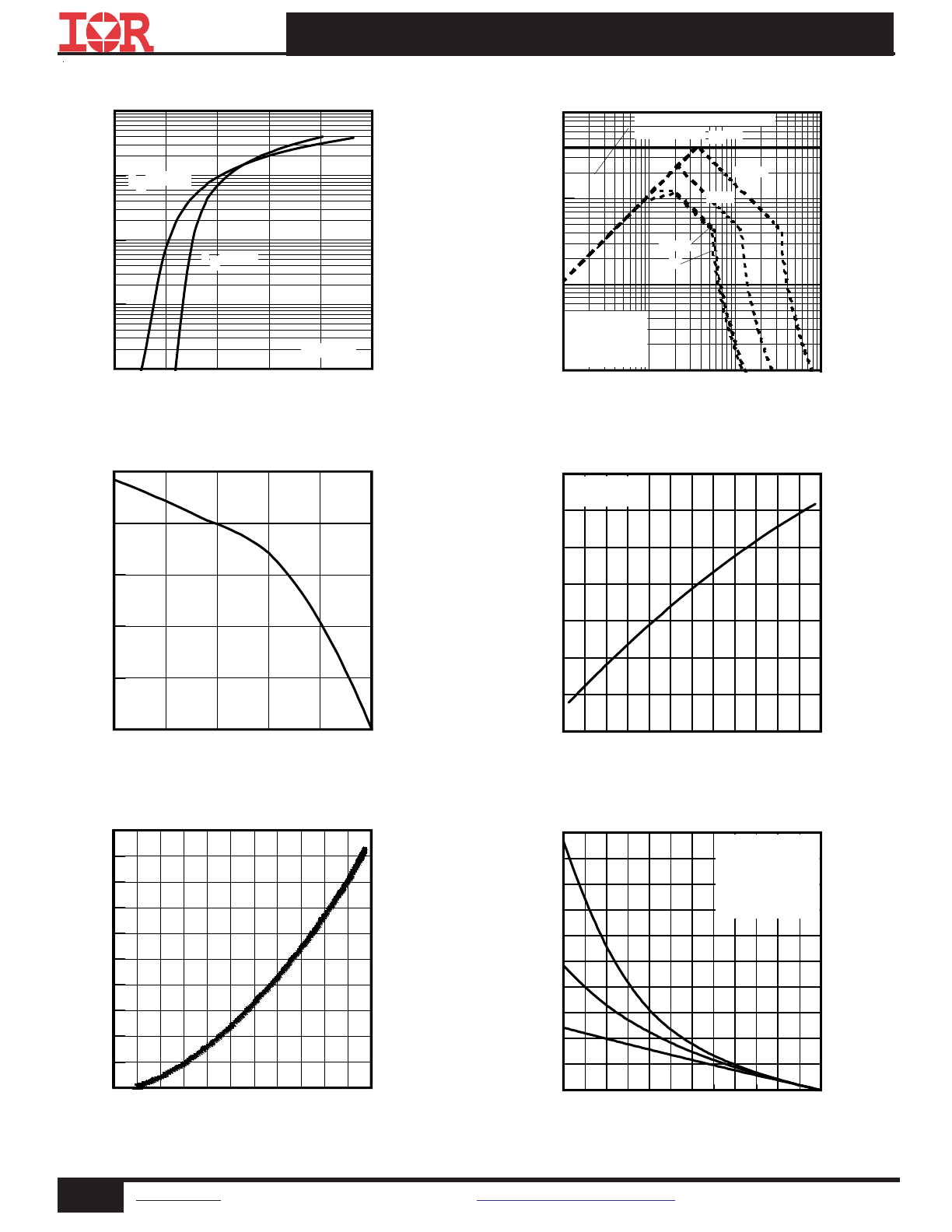
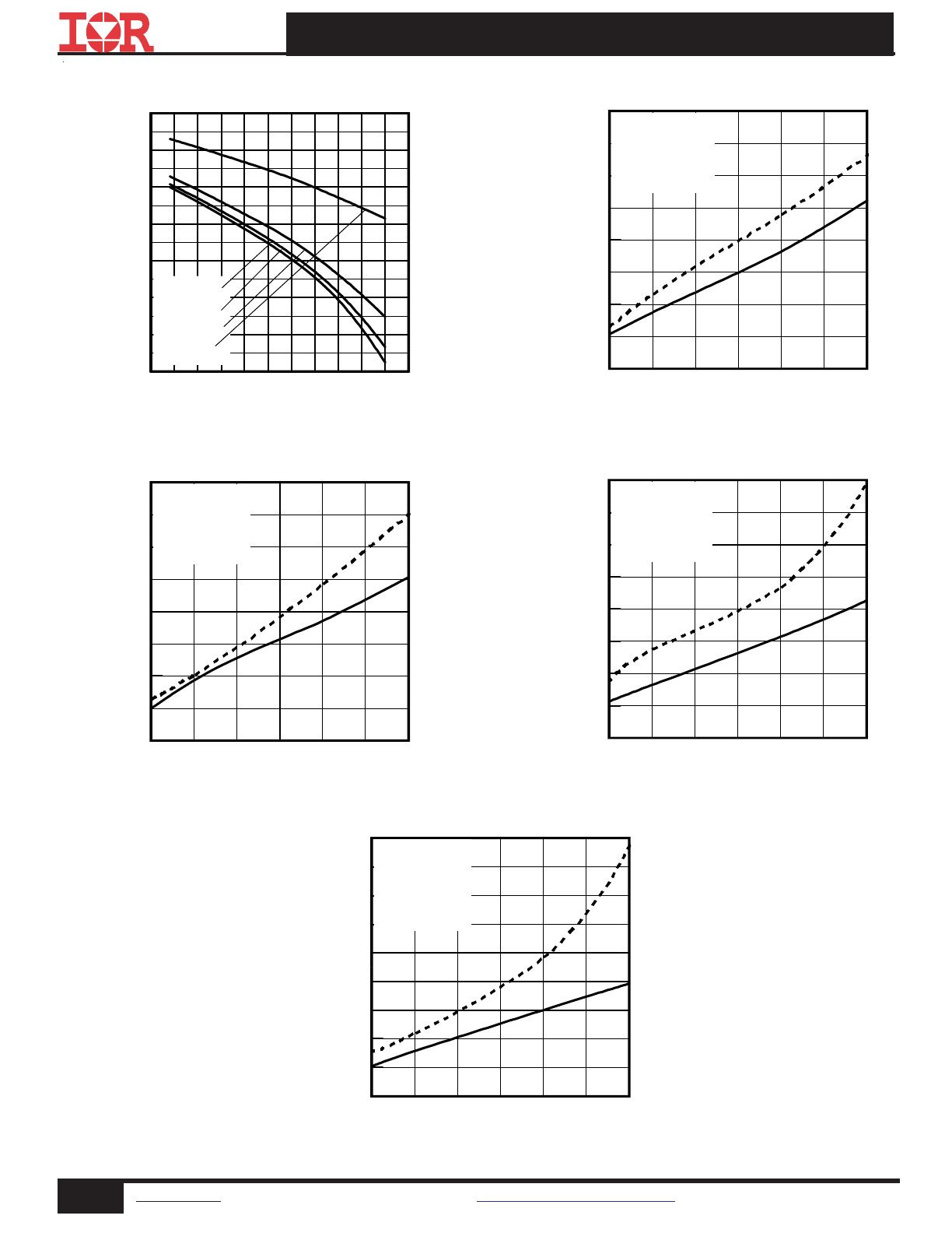
Fig 8. Maximum Safe Operating Area
Fig 10. Drain-to-Source Breakdown Voltage
Fig 7. Typical Source-Drain Diode
Forward Voltage
Fig 11. Typical C
OSS
Stored Energy
Fig 9. Maximum Drain Current vs.
Case Temperature
Fig 12. Maximum Avalanche Energy vs. DrainCurrent
-60 -40 -20 0 20 40 60 80 100120140160180
TJ , Temperature ( °C )
90
95
100
105
110
115
120
125
V
(B
R
)D
S
S
, D
ra
in
-t
o-
S
ou
rc
e
B
re
ak
do
w
n
V
ol
ta
ge
(
V
)
Id = 5mA
-10 0 10 20 30 40 50 60 70 80 90 100
VDS, Drain-to-Source Voltage (V)
0.0
0.2
0.4
0.6
0.8
1.0
1.2
1.4
1.6
1.8
2.0
E
ne
rg
y
(μ
J)
0.0
0.5
1.0
1.5
2.0
2.5
VSD, Source-to-Drain Voltage (V)
0.1
1
10
100
1000
I S
D
, R
ev
er
se
D
ra
in
C
ur
re
nt
(
A
)
TJ = 25°C
TJ = 175°C
VGS = 0V
0
1
10
100
VDS, Drain-to-Source Voltage (V)
1
10
100
1000
I D
,
D
ra
in
-t
o-
S
ou
rc
e
C
ur
re
nt
(
A
)
OPERATION IN THIS AREA
LIMITED BY R DS(on)
Tc = 25°C
Tj = 175°C
Single Pulse
100μsec
1msec
10msec
DC
25
50
75
100
125
150
175
Starting TJ , Junction Temperature (°C)
0
100
200
300
400
500
600
700
800
900
1000
E
A
S
,
S
in
gl
e
P
ul
se
A
va
la
nc
he
E
ne
rg
y
(m
J)
ID
TOP 6.4A
9.4A
BOTTOM 58A
25
50
75
100
125
150
TC , Case Temperature (°C)
0
20
40
60
80
100
I D
,
D
ra
in
C
ur
re
nt
(
A
)
5
www.irf.com
©
2014 International Rectifier
Submit Datasheet Feedback
April 25, 2014
IRFB4410ZPbF/IRFS4410ZPbF/IRFSL4410ZPbF
Fig 13. Maximum Effective Transient Thermal Impedance, Junction-to-Case
Fig 14. Typical Avalanche Current vs.Pulsewidth
Fig 15. Maximum Avalanche Energy vs. Temperature
Notes on Repetitive Avalanche Curves , Figures 14, 15:
(For further info, see AN-1005 at www.irf.com)
1. Avalanche failures assumption:
Purely a thermal phenomenon and failure occurs at a temperature far in
excess of T
jmax
. This is validated for every part type.
2. Safe operation in Avalanche is allowed as long asT
jmax
is not exceeded.
3. Equation below based on circuit and waveforms shown in Figures 16a, 16b.
4. P
D (ave)
= Average power dissipation per single avalanche pulse.
5. BV = Rated breakdown voltage (1.3 factor accounts for voltage increase
during avalanche).
6. I
av
= Allowable avalanche current.
7.
ΔT
=
Allowable rise in junction temperature, not to exceed
T
jmax
(assumed as
25°C in Figure 14, 15).
t
av =
Average time in avalanche.
D = Duty cycle in avalanche = t
av
·f
Z
thJC
(D, t
av
) = Transient thermal resistance, see Figures 13)
P
D (ave)
= 1/2 ( 1.3·BV·I
av
) =
DT/ Z
thJC
I
av
=
2
DT/ [1.3·BV·Z
th
]
E
AS (AR)
= P
D (ave)
·t
av
1E-006
1E-005
0.0001
0.001
0.01
0.1
t1 , Rectangular Pulse Duration (sec)
0.001
0.01
0.1
1
T
he
rm
al
R
es
po
ns
e
(
Z
th
JC
)
°
C
/W
0.20
0.10
D = 0.50
0.02
0.01
0.05
SINGLE PULSE
( THERMAL RESPONSE )
Notes:
1. Duty Factor D = t1/t2
2. Peak Tj = P dm x Zthjc + Tc
τ
J
τ
J
τ
1
τ
1
τ
2
τ
2
R
1
R
1
R
2
R
2
τ
τ
C
Ci i
/Ri
Ci=
τi/Ri
Ri (°C/W)
τi (sec)
0.237 0.000178
0.413 0.003772
25
50
75
100
125
150
175
Starting TJ , Junction Temperature (°C)
0
50
100
150
E
A
R
,
A
va
la
nc
he
E
ne
rg
y
(m
J)
TOP Single Pulse
BOTTOM 1.0% Duty Cycle
ID = 58A
1.0E-06
1.0E-05
1.0E-04
1.0E-03
1.0E-02
1.0E-01
tav (sec)
0.1
1
10
100
A
va
la
nc
he
C
ur
re
nt
(
A
)
0.05
Duty Cycle = Single Pulse
0.10
Allowed avalanche Current vs avalanche
pulsewidth, tav, assuming
ΔΤ j = 25°C and
Tstart = 150°C.
0.01
Allowed avalanche Current vs avalanche
pulsewidth, tav, assuming
Δ Tj = 150°C and
Tstart =25°C (Single Pulse)
6
www.irf.com
©
2014 International Rectifier
Submit Datasheet Feedback
April 25, 2014
IRFB4410ZPbF/IRFS4410ZPbF/IRFSL4410ZPbF
Fig. 17 - Typical Recovery Current vs. di
f
/dt
Fig 16. Threshold Voltage vs. Temperature
Fig. 19 - Typical Stored Charge vs. di
f
/dt
Fig. 18 - Typical Recovery Current vs. di
f
/dt
Fig. 20 - Typical Stored Charge vs. di
f
/dt
-75 -50 -25 0 25 50 75 100 125 150 175 200
TJ , Temperature ( °C )
1.0
1.5
2.0
2.5
3.0
3.5
4.0
4.5
V
G
S
(t
h)
, G
at
e
th
re
sh
ol
d
V
ol
ta
ge
(
V
)
ID = 150μA
ID = 250μA
ID = 1.0mA
ID = 1.0A
100
200
300
400
500
600
700
dif/dt (A/μs)
0
50
100
150
200
250
300
350
400
450
Q
rr
(
nC
)
IF = 58A
VR = 85V
TJ = 25°C _____
TJ = 125°C
----------
100
200
300
400
500
600
700
dif/dt (A/μs)
0
50
100
150
200
250
300
350
400
Q
rr
(
nC
)
IF = 39A
VR = 85V
TJ = 25°C _____
TJ = 125°C ----------
100
200
300
400
500
600
700
dif/dt (A/μs)
0
5
10
15
20
I R
R
M
(
A
)
IF = 58A
VR = 85V
TJ = 25°C _____
TJ = 125°C ----------
100
200
300
400
500
600
700
dif/dt (A/μs)
0
5
10
15
20
I R
R
M
(
A
)
IF = 39A
VR = 85V
TJ = 25°C _____
TJ = 125°C ----------
7
www.irf.com
©
2014 International Rectifier
Submit Datasheet Feedback
April 25, 2014
IRFB4410ZPbF/IRFS4410ZPbF/IRFSL4410ZPbF
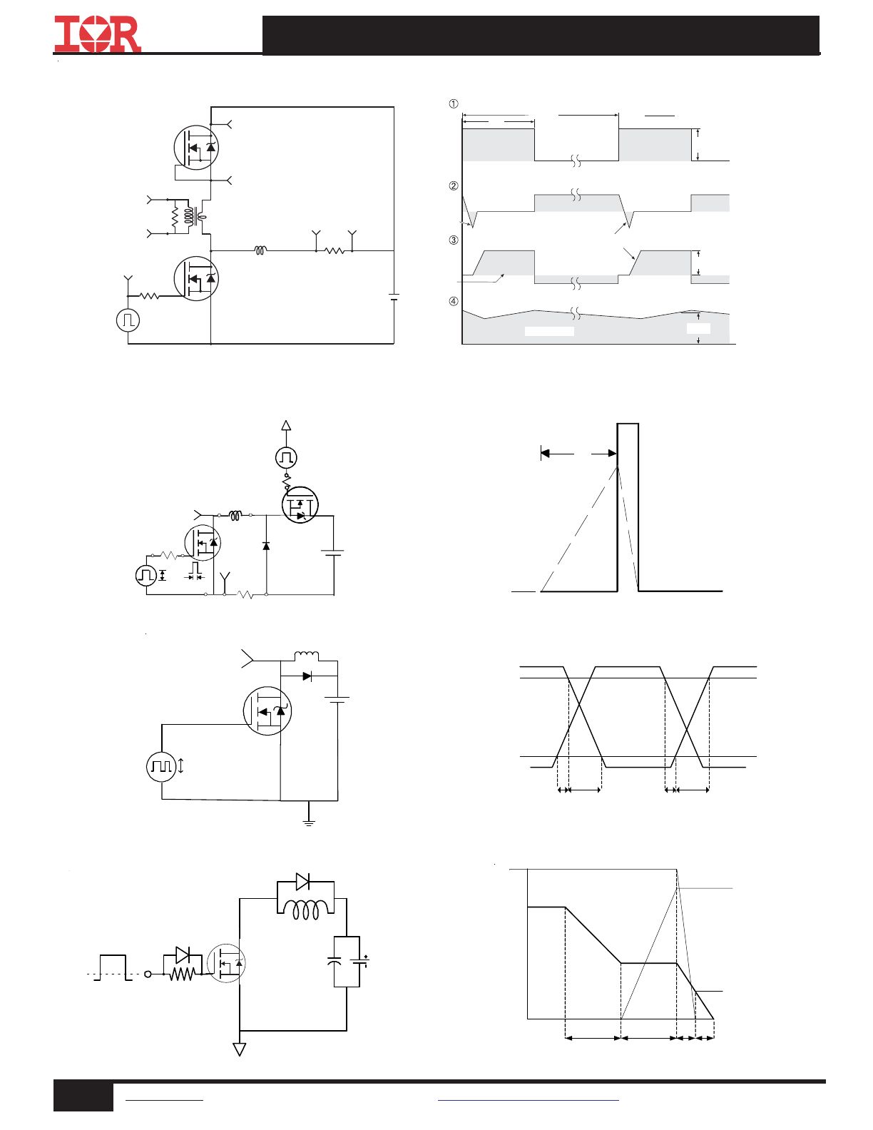
Fig 23a. Switching Time Test Circuit
Fig 23b. Switching Time Waveforms
Fig 22b. Unclamped Inductive Waveforms
Fig 22a. Unclamped Inductive Test Circuit
Fig 24a. Gate Charge Test Circuit
Fig 24b. Gate Charge Waveform
Fig 21.
Peak Diode Recovery dv/dt Test Circuit for N-Channel
HEXFET
®
Power MOSFETs
Circuit Layout Considerations
• Low Stray Inductance
• Ground Plane
• Low Leakage Inductance
Current Transformer
P.W.
Period
di/dt
Diode Recovery
dv/dt
Ripple
≤ 5%
Body Diode Forward Drop
Re-Applied
Voltage
Reverse
Recovery
Current
Body Diode Forward
Current
V
GS
=10V
V
DD
I
SD
Driver Gate Drive
D.U.T. I
SD
Waveform
D.U.T. V
DS
Waveform
Inductor Curent
D =
P.W.
Period
*
V
GS
= 5V for Logic Level Devices
*
+
-
+
+
+
-
-
-
R
G
V
DD
• dv/dt controlled by R
G
• Driver same type as D.U.T.
• I
SD
controlled by Duty Factor "D"
• D.U.T. - Device Under Test
D.U.T
Inductor Current
1K
VCC
DUT
0
L
S
20K
Vds
Vgs
Id
Vgs(th)
Qgs1
Qgs2
Qgd
Qgodr
RG
IAS
0.01
Ω
tp
D.U.T
L
VDS
+
- VDD
DRIVER
A
15V
20V
tp
V
(BR)DSS
I
AS
V
GS
V
DD
V
DS
L
D
D.U.T
+
-
Second Pulse Width < 1μs
Duty Factor < 0.1%
V
GS
V
DS
90%
10%
t
d(on)
t
d(off)
t
r
t
f
8
www.irf.com
©
2014 International Rectifier
Submit Datasheet Feedback
April 25, 2014
IRFB4410ZPbF/IRFS4410ZPbF/IRFSL4410ZPbF
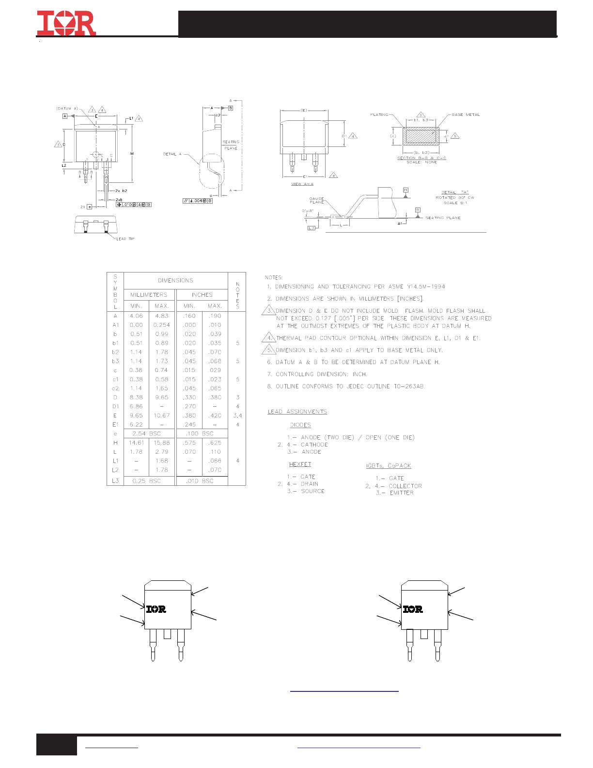
TO-220AB Package Outline
Dimensions are shown in millimeters (inches)
TO-220AB Part Marking Information
TO-220AB packages are not recommended for Surface Mount Application.
Note: For the most current drawing please refer to IR website at:
http://www.irf.com/package/
FB4410Z
FB4410Z
PYWW?
LC LC
PART NUMBER
DATE CODE
P = LEAD-FREE
Y = LAST DIGIT OF YEAR
WW = WORK WEEK
? = ASSEMBLY SITE CODE
INTERNATIONAL
RECTIFIER LOGO
ASSEMBLY
LOT CODE
OR
YWWP
LC LC
PART NUMBER
DATE CODE
Y = LAST DIGIT OF YEAR
WW = WORK WEEK
P = LEAD-FREE
INTERNATIONAL
RECTIFIER LOGO
ASSEMBLY
LOT CODE
9
www.irf.com
©
2014 International Rectifier
Submit Datasheet Feedback
April 25, 2014
IRFB4410ZPbF/IRFS4410ZPbF/IRFSL4410ZPbF
Note: For the most current drawing please refer to IR website at:
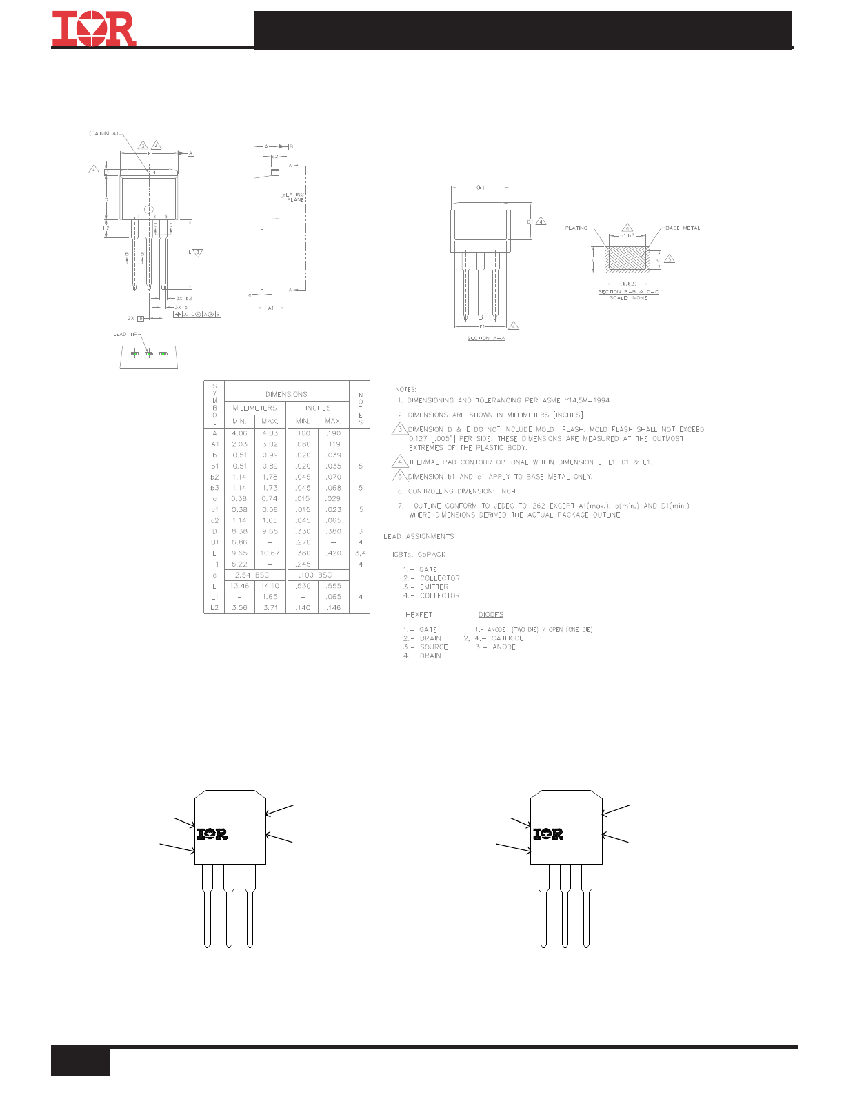
http://www.irf.com/package/
D
2
Pak Package Outline
(Dimensions are shown in millimeters (inches))
D
2
Pak Part Marking Information
IRFS4410Z
FS4410Z
PYWW?
YWWP
ASSEMBLY
LOT CODE
INTERNATIONAL
RECTIFIER LOGO
DATE CODE
P = LEAD-FREE
Y = LAST DIGIT OF YEAR
WW = WORK WEEK
? = ASSEMBLY SITE CODE
LC LC
PART NUMBER
OR
ASSEMBLY
LOT CODE
INTERNATIONAL
RECTIFIER LOGO
DATE CODE
Y = LAST DIGIT OF YEAR
WW = WORK WEEK
P = LEAD-FREE
LC LC
PART NUMBER
10
www.irf.com
©
2014 International Rectifier
Submit Datasheet Feedback
April 25, 2014
IRFB4410ZPbF/IRFS4410ZPbF/IRFSL4410ZPbF
TO-262 Part Marking Information
TO-262 Package Outline
(Dimensions are shown in millimeters (inches))
Note: For the most current drawing please refer to IR website at:
http://www.irf.com/package/
FSL4410Z
PYWW?
FSL4410Z
YWWP
ASSEMBLY
LOT CODE
INTERNATIONAL
RECTIFIER LOGO
DATE CODE
P = LEAD-FREE
Y = LAST DIGIT OF YEAR
WW = WORK WEEK
? = ASSEMBLY SITE CODE
PART NUMBER
OR
DATE CODE
Y = LAST DIGIT OF YEAR
WW = WORK WEEK
P = LEAD-FREE
LC LC
ASSEMBLY
LOT CODE
INTERNATIONAL
RECTIFIER LOGO
PART NUMBER
LC LC