
HEXFET
®
Power MOSFET
Notes
through
are on page 10
Applications
l
Synchronous MOSFET for Notebook Processor Power
l
Synchronous Rectifier MOSFET for Isolated DC-DC Converters
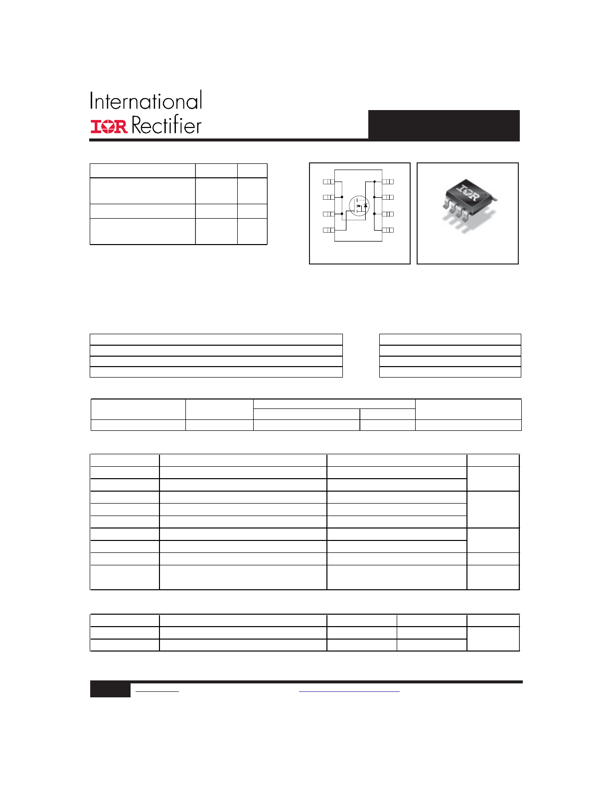
Top View
8
1
2
3
4
5
6
7
D
D
D
D
G
S
A
S
S
A
SO-8
Absolute Maximum Ratings
Parameter
Units
V
DS
Drain-to-Source Voltage
V
GS
Gate-to-Source Voltage
I
D
@ T
A
= 25°C
Continuous Drain Current, V
GS
@ 10V
I
D
@ T
A
= 70°C
Continuous Drain Current, V
GS
@ 10V
I
DM
Pulsed Drain Current
c
P
D
@T
A
= 25°C
Power Dissipation
P
D
@T
A
= 70°C
Power Dissipation
Linear Derating Factor
W/°C
T
J
Operating Junction and
T
STG
Storage Temperature Range
Thermal Resistance
Parameter
Typ.
Max.
Units
R
θJL
Junction-to-Drain Lead
g
–––
20
R
θJA
Junction-to-Ambient
fg
–––
50
-55 to + 150
2.5
0.02
1.6
Max.
25
20
200
±20
25
°C/W
V
A
W
°C
IRF8252TRPbF-1
Features
Benefits
Industry-standard pinout SO-8 Package
⇒
Multi-Vendor Compatibility
Compatible with Existing Surface Mount Techniques
Easier Manufacturing
RoHS Compliant, Halogen-Free
Environmentally Friendlier
MSL1, Industrial qualification
Increased Reliability
V
DS
25
V
R
DS(on) max
(@V
GS
= 10V)
2.7
Q
g (typical)
35
nC
I
D
(@T
A
= 25°C)
25
A
mΩ
1
www.irf.com
©
2014 International Rectifier
Submit Datasheet Feedback
October 16, 2014
Form
Quantity
IRF8252PbF-1
SO-8
Tape and Reel
4000
IRF8252TRPbF-1
Package Type
Standard Pack
Orderable Part Number
Base Part Number
IRF8252TRPbF-1
2
www.irf.com
©
2014 International Rectifier
Submit Datasheet Feedback
October 16, 2014
S
D
G
Static @ T
J
= 25°C (unless otherwise specified)
Parameter
Min. Typ. Max. Units
BV
DSS
Drain-to-Source Breakdown Voltage
25
–––
–––
V
ΔΒV
DSS
/
ΔT
J
Breakdown Voltage Temp. Coefficient
–––
0.018
–––
V/°C
R
DS(on)
Static Drain-to-Source On-Resistance
–––
2.0
2.7
–––
2.9
3.7
V
GS(th)
Gate Threshold Voltage
1.35
1.80
2.35
V
ΔV
GS(th)
Gate Threshold Voltage Coefficient
–––
-6.67
––– mV/°C
I
DSS
Drain-to-Source Leakage Current
–––
–––
1.0
–––
–––
150
I
GSS
Gate-to-Source Forward Leakage
–––
–––
100
Gate-to-Source Reverse Leakage
–––
–––
-100
gfs
Forward Transconductance
89
–––
–––
S
Q
g
Total Gate Charge
–––
35
53
Q
gs1
Pre-Vth Gate-to-Source Charge
–––
10
–––
Q
gs2
Post-Vth Gate-to-Source Charge
–––
4.6
–––
Q
gd
Gate-to-Drain Charge
–––
12
–––
Q
godr
Gate Charge Overdrive
–––
8.9
–––
See Figs. 15 & 16
Q
sw
Switch Charge (Q
gs2
+ Q
gd
)
–––
16
–––
Q
oss
Output Charge
–––
26
–––
nC
R
g
Gate Resistance
–––
0.61
1.22
Ω
t
d(on)
Turn-On Delay Time
–––
23
–––
t
r
Rise Time
–––
32
–––
t
d(off)
Turn-Off Delay Time
–––
19
–––
t
f
Fall Time
–––
12
–––
C
iss
Input Capacitance
–––
5305
–––
C
oss
Output Capacitance
–––
1340
–––
C
rss
Reverse Transfer Capacitance
–––
725
–––
Avalanche Characteristics
Parameter
Units
E
AS
Single Pulse Avalanche Energy
d
mJ
I
AR
Avalanche Current
c
A
Diode Characteristics
Parameter
Min. Typ. Max. Units
I
S
Continuous Source Current
–––
–––
(Body Diode)
I
SM
Pulsed Source Current
–––
–––
(Body Diode)
c
V
SD
Diode Forward Voltage
–––
–––
1.0
V
t
rr
Reverse Recovery Time
–––
19
29
ns
Q
rr
Reverse Recovery Charge
–––
12
18
nC
t
on
Forward Turn-On Time
Intrinsic turn-on time is negligible (turn-on is dominated by LS+LD)
m
Ω
A
3.1
200
A
–––
I
D
= 20A
V
GS
= 0V
V
DS
= 13V
nC
ns
pF
V
GS
= 4.5V, I
D
= 20A
e
V
GS
= 4.5V
Typ.
–––
V
DS
= V
GS
, I
D
= 100μA
R
G
= 1.8
Ω
V
DS
= 13V, I
D
= 20A
V
DS
= 20V, V
GS
= 0V, T
J
= 125°C
μA
nA
T
J
= 25°C, I
F
= 20A, V
DD
= 13V
di/dt = 230A/μs
e
T
J
= 25°C, I
S
= 20A, V
GS
= 0V
e
showing the
integral reverse
p-n junction diode.
MOSFET symbol
V
DS
= V
GS
, I
D
= 100μA
V
DS
= 16V, V
GS
= 0V
V
DD
= 13V, V
GS
= 4.5V
I
D
= 20A
V
DS
= 13V
V
GS
= 20V
V
GS
= -20V
V
DS
= 20V, V
GS
= 0V
Conditions
V
GS
= 0V, I
D
= 250μA
Reference to 25°C, I
D
= 1mA
V
GS
= 10V, I
D
= 25A
e
Conditions
See Fig. 18
Max.
231
20
ƒ = 1.0MHz
3
www.irf.com
©
2014 International Rectifier
Submit Datasheet Feedback
October 16, 2014
IRF8252TRPbF-1
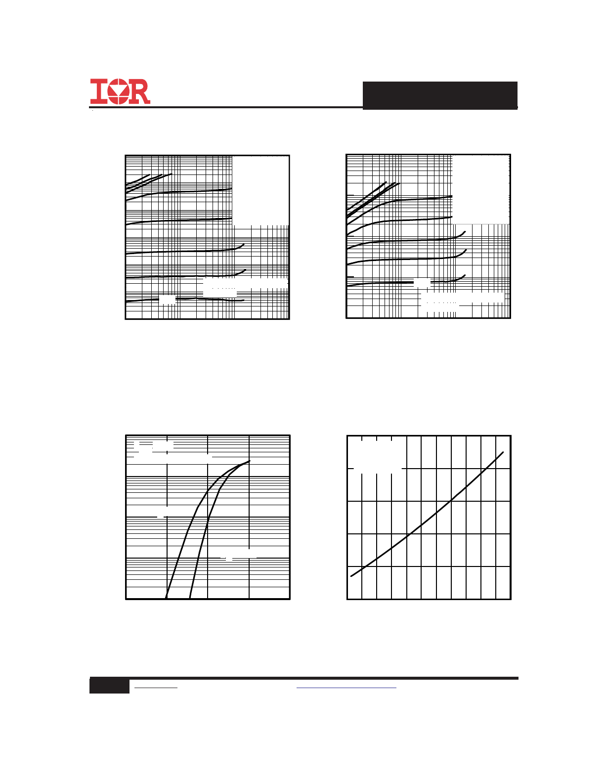
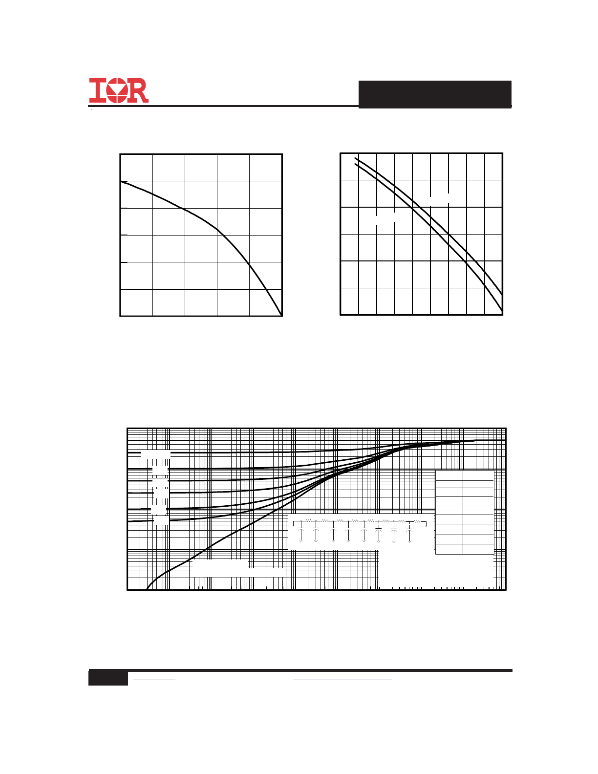
Fig 4. Normalized On-Resistance
vs. Temperature
Fig 2. Typical Output Characteristics
Fig 1. Typical Output Characteristics
Fig 3. Typical Transfer Characteristics
1
2
3
4
5
VGS, Gate-to-Source Voltage (V)
0.1
1
10
100
1000
I D
, D
ra
in
-t
o-
S
ou
rc
e
C
ur
re
nt
(
A
)
TJ = 25°C
TJ = 150°C
VDS = 15V
≤60μs PULSE WIDTH
-60 -40 -20 0 20 40 60 80 100 120 140 160
TJ , Junction Temperature (°C)
0.6
0.8
1.0
1.2
1.4
1.6
R
D
S
(o
n)
,
D
ra
in
-t
o-
S
ou
rc
e
O
n
R
es
is
ta
nc
e
(
N
or
m
al
iz
ed
)
ID = 25A
VGS = 10V
0.1
1
10
100
VDS, Drain-to-Source Voltage (V)
0.001
0.01
0.1
1
10
100
1000
I D
, D
ra
in
-t
o-
S
ou
rc
e
C
ur
re
nt
(
A
)
VGS
TOP
10V
5.0V
4.5V
3.5V
3.0V
2.7V
2.5V
BOTTOM
2.3V
≤60μs PULSE WIDTH
Tj = 25°C
2.3V
0.1
1
10
100
VDS, Drain-to-Source Voltage (V)
0.1
1
10
100
1000
I D
, D
ra
in
-t
o-
S
ou
rc
e
C
ur
re
nt
(
A
)
2.3V
≤60μs PULSE WIDTH
Tj = 150°C
VGS
TOP
10V
5.0V
4.5V
3.5V
3.0V
2.7V
2.5V
BOTTOM
2.3V
IRF8252TRPbF-1
4
www.irf.com
©
2014 International Rectifier
Submit Datasheet Feedback
October 16, 2014
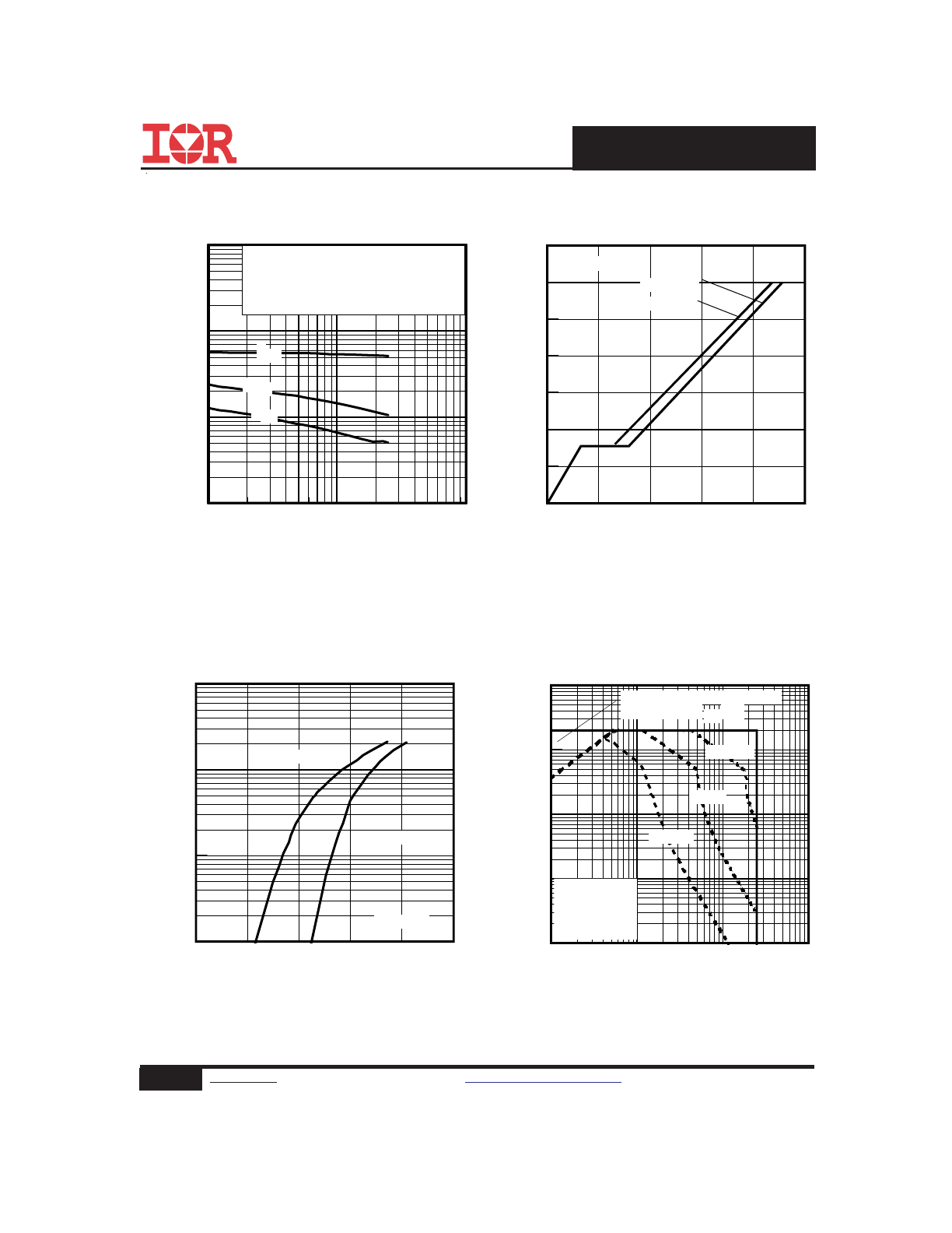
Fig 8. Maximum Safe Operating Area
Fig 6. Typical Gate Charge vs.
Gate-to-Source Voltage
Fig 5. Typical Capacitance vs.
Drain-to-Source Voltage
Fig 7. Typical Source-Drain Diode
Forward Voltage
0
20
40
60
80
100
QG, Total Gate Charge (nC)
0.0
2.0
4.0
6.0
8.0
10.0
12.0
14.0
V
G
S
, G
at
e-
to
-S
ou
rc
e
V
ol
ta
ge
(
V
)
VDS= 20V
VDS= 13V
ID= 20A
0.2
0.4
0.6
0.8
1.0
1.2
VSD, Source-to-Drain Voltage (V)
1.0
10
100
1000
I S
D
, R
ev
er
se
D
ra
in
C
ur
re
nt
(
A
)
TJ = 25°C
TJ = 150°C
VGS = 0V
1
10
100
VDS, Drain-to-Source Voltage (V)
100
1000
10000
100000
C
, C
ap
ac
ita
nc
e
(p
F
)
VGS = 0V, f = 1 MHZ
Ciss = Cgs + Cgd, C ds SHORTED
Crss = Cgd
Coss = Cds + Cgd
Coss
Crss
Ciss
0
1
10
100
VDS, Drain-to-Source Voltage (V)
0.1
1
10
100
1000
I D
,
D
ra
in
-t
o-
S
ou
rc
e
C
ur
re
nt
(
A
)
OPERATION IN THIS AREA
LIMITED BY R DS(on)
TA = 25°C
Tj = 150°C
Single Pulse
100μsec
1msec
10msec
5
www.irf.com
©
2014 International Rectifier
Submit Datasheet Feedback
October 16, 2014
IRF8252TRPbF-1
Fig 11. Maximum Effective Transient Thermal Impedance, Junction-to-Ambient
Fig 9. Maximum Drain Current vs.
Ambient Temperature
Fig 10. Threshold Voltage vs. Temperature
25
50
75
100
125
150
TA , Ambient Temperature (°C)
0
5
10
15
20
25
30
I D
,
D
ra
in
C
ur
re
nt
(
A
)
-75 -50 -25
0
25
50
75 100 125 150
TJ , Temperature ( °C )
1.0
1.5
2.0
2.5
V
G
S
(t
h)
, G
at
e
T
hr
es
ho
ld
V
ol
ta
ge
(
V
)
ID = 250μA
ID = 100μA
1E-006
1E-005
0.0001
0.001
0.01
0.1
1
10
100
1000
t1 , Rectangular Pulse Duration (sec)
0.01
0.1
1
10
100
T
he
rm
al
R
es
po
ns
e
(
Z
th
JA
)
°
C
/W
0.20
0.10
D = 0.50
0.02
0.01
0.05
SINGLE PULSE
( THERMAL RESPONSE )
Notes:
1. Duty Factor D = t1/t2
2. Peak Tj = P dm x Zthja + TA
τ
J
τ
J
τ
1
τ
1
τ
2
τ
2
τ
3
τ
3
R
1
R
1
R
2
R
2
R
3
R
3
Ci=
τi/Ri
Ci=
τi/Ri
τ
4
τ
4
R
4
R
4
τ
A
τ
A
R
8
R
8
τ
5
τ
5
R
5
R
5
τ
6
τ
6
R
6
R
6
τ
7
τ
7
R
7
R
7
0.02127 0.000002
0.02040 0.000006
0.21216 0.000082
0.79696 0.001560
6.31529 0.028913
0.45152 0.006475
26.2230 1.208856
16.5590 45.68988
Ri (°C/W)
τi (sec)
IRF8252TRPbF-1
6
www.irf.com
©
2014 International Rectifier
Submit Datasheet Feedback
October 16, 2014
Fig 13. Maximum Avalanche Energy
vs. Drain Current
Fig 12. On-Resistance vs. Gate Voltage
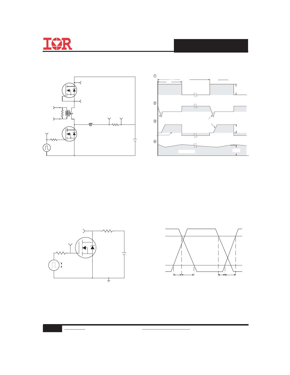
Fig 15. Gate Charge Test Circuit
1K
VCC
DUT
0
L
S
20K
Fig 14. Unclamped Inductive Test Circuit
and Waveform
tp
V
(BR)DSS
I
AS
RG
IAS
0.01
Ω
tp
D.U.T
L
VDS
+
- VDD
DRIVER
A
15V
20V
Fig 16. Gate Charge Waveform
Vds
Vgs
Id
Vgs(th)
Qgs1
Qgs2
Qgd
Qgodr
25
50
75
100
125
150
Starting TJ , Junction Temperature (°C)
0
100
200
300
400
500
600
700
800
900
1000
E
A
S
,
S
in
gl
e
P
ul
se
A
va
la
nc
he
E
ne
rg
y
(m
J)
ID
TOP 2.45A
8.0A
BOTTOM 20A
2
4
6
8
10
VGS, Gate -to -Source Voltage (V)
1
2
3
4
5
6
7
R
D
S
(o
n)
,
D
ra
in
-t
o
-S
ou
rc
e
O
n
R
es
is
ta
nc
e
(m
Ω
)
ID = 20A
TJ = 25°C
TJ = 125°C
7
www.irf.com
©
2014 International Rectifier
Submit Datasheet Feedback
October 16, 2014
IRF8252TRPbF-1
Fig 17.
Peak Diode Recovery dv/dt Test Circuit for N-Channel
HEXFET
®
Power MOSFETs
Circuit Layout Considerations
• Low Stray Inductance
• Ground Plane
• Low Leakage Inductance
Current Transformer
P.W.
Period
di/dt
Diode Recovery
dv/dt
Ripple
≤ 5%
Body Diode Forward Drop
Re-Applied
Voltage
Reverse
Recovery
Current
Body Diode Forward
Current
V
GS
=10V
V
DD
I
SD
Driver Gate Drive
D.U.T. I
SD
Waveform
D.U.T. V
DS
Waveform
Inductor Curent
D =
P.W.
Period
*
V
GS
= 5V for Logic Level Devices
*
+
-
+
+
+
-
-
-
R
G
V
DD
• dv/dt controlled by R
G
• Driver same type as D.U.T.
• I
SD
controlled by Duty Factor "D"
• D.U.T. - Device Under Test
D.U.T
Fig 18b. Switching Time Waveforms
Fig 18a. Switching Time Test Circuit
V
DS
90%
10%
V
GS
t
d(on)
t
r
t
d(off)
t
f
V
DS
Pulse Width ≤ 1 µs
Duty Factor ≤ 0.1 %
R
D
V
GS
R
G
D.U.T.
V
GS
+
-
V
DD
IRF8252TRPbF-1
8
www.irf.com
©
2014 International Rectifier
Submit Datasheet Feedback
October 16, 2014
Note: For the most current drawing please refer to IR website at
http://www.irf.com/package/
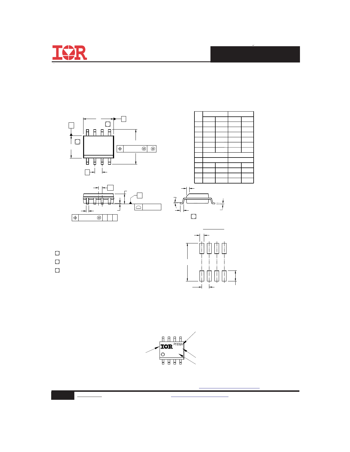
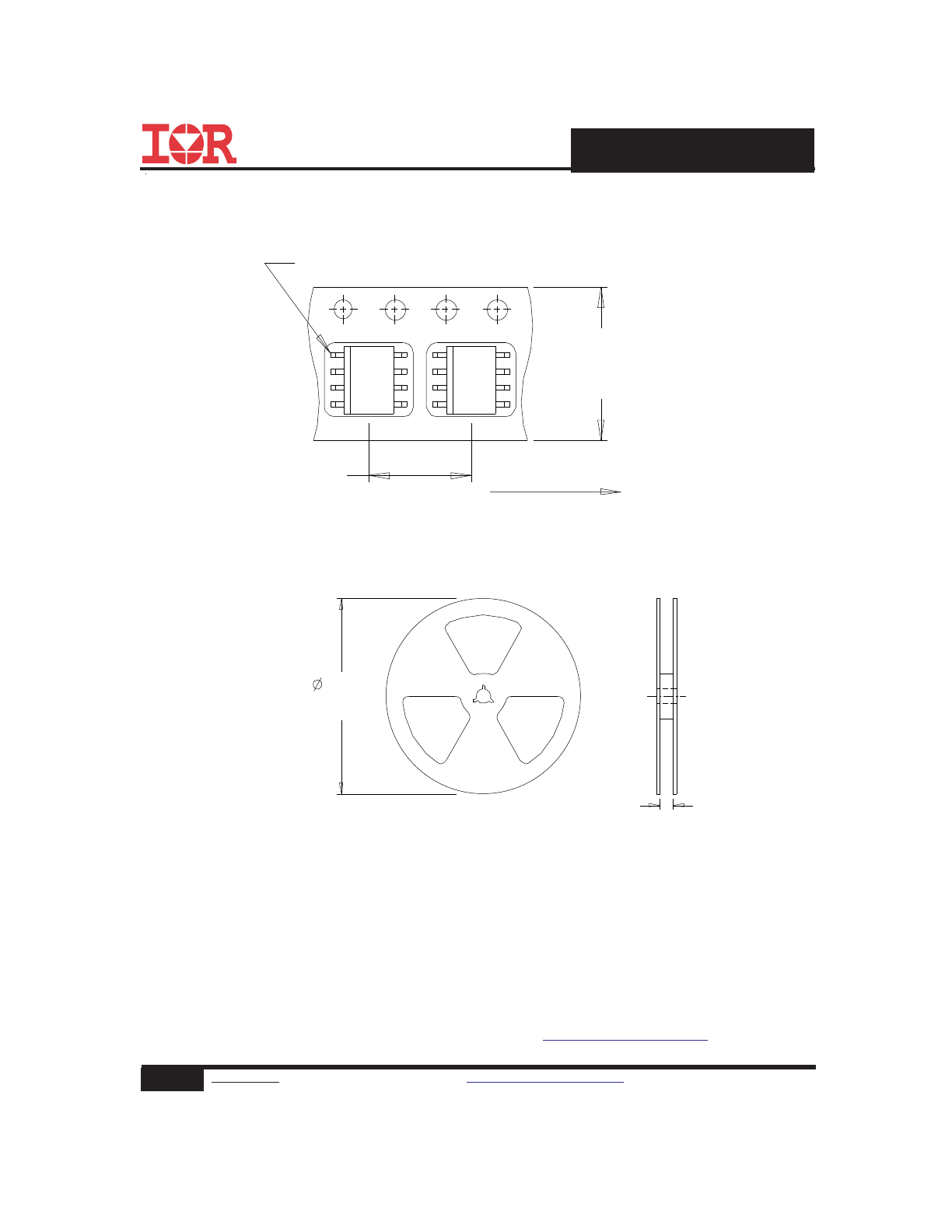
SO-8 Package Outline
(Mosfet & Fetky)
e 1
D
E
y
b
A
A1
H
K
L
.189
.1497
0°
.013
.050 BASIC
.0532
.0040
.2284
.0099
.016
.1968
.1574
8°
.020
.0688
.0098
.2440
.0196
.050
4.80
3.80
0.33
1.35
0.10
5.80
0.25
0.40
0°
1.27 BASIC
5.00
4.00
0.51
1.75
0.25
6.20
0.50
1.27
MIN
MAX
MILLIMETERS
INCHES
MIN
MAX
DIM
8°
e
c
.0075
.0098
0.19
0.25
.025 BASIC
0.635 BASIC
8
7
5
6
5
D
B
E
A
e
6X
H
0.25 [.010]
A
6
7
K x 45°
8X L
8X c
y
0.25 [.010]
C A B
e1
A
A1
8X b
C
0.10 [.004]
4
3
1
2
FOOTPRINT
8X 0.72 [.028]
6.46 [.255]
3X 1.27 [.050]
8X 1.78 [.070]
4. OUTLINE CONFORMS TO JEDEC OUTLINE MS-012AA.
NOTES:
1. DIMENSIONING & TOLERANCING PER ASME Y14.5M-1994.
2. CONTROLLING DIMENSION: MILLIMETER
3. DIMENSIONS ARE SHOWN IN MILLIMETERS [INCHES].
5 DIMENSION DOES NOT INCLUDE MOLD PROT RUSIONS.
6 DIMENSION DOES NOT INCLUDE MOLD PROT RUSIONS.
MOLD PROTRUSIONS NOT TO EXCEED 0.25 [.010].
7 DIMENSION IS THE LENGT H OF LEAD FOR SOLDERING TO
A SUBSTRATE.
MOLD PROTRUSIONS NOT TO EXCEED 0.15 [.006].
Dimensions are shown in milimeters (inches)
SO-8 Part Marking Information
P = DISGNATES LEAD - FREE
EXAMPLE: THIS IS AN IRF7101 (MOSFET)
F7101
XXXX
INTERNATIONAL
LOGO
RECTIFIER
PART NUMBER
LOT CODE
PRODUCT (OPTIONAL)
DATE CODE (YWW)
Y = LAST DIGIT OF THE YEAR
WW = WEEK
A = ASSEMBLY SITE CODE
9
www.irf.com
©
2014 International Rectifier
Submit Datasheet Feedback
October 16, 2014
IRF8252TRPbF-1
330.00
(12.992)
MAX.
14.40 ( .566 )
12.40 ( .488 )
NOTES :
1. CONTROLLING DIMENSION : MILLIMETER.
2. OUTLINE CONFORMS TO EIA-481 & EIA-541.
FEED DIRECTION
TERMINAL NUMBER 1
12.3 ( .484 )
11.7 ( .461 )
8.1 ( .318 )
7.9 ( .312 )
NOTES:
1. CONTROLLING DIMENSION : MILLIMETER.
2. ALL DIMENSIONS ARE SHOWN IN MILLIMETERS(INCHES).
3. OUTLINE CONFORMS TO EIA-481 & EIA-541.
SO-8 Tape and Reel
(Dimensions are shown in milimeters (inches))
Note: For the most current drawing please refer to IR website at
http://www.irf.com/package/
IRF8252TRPbF-1
10
www.irf.com
©
2014 International Rectifier
Submit Datasheet Feedback
October 16, 2014
Notes:
Repetitive rating; pulse width limited by max. junction temperature.
Starting T
J
= 25°C, L = 1.12mH, R
G
= 25
Ω, I
AS
= 20A.
Pulse width ≤ 400μs; duty cycle ≤ 2%.
When mounted on 1 inch square copper board.
R
θ
is measured at
T
J
of approximately 90°C.
† Qualification standards can be found at International Rectifier’s web site:
http://www.irf.com/product-info/reliability
††
Applicable version of JEDEC standard at the time of product release
IR WORLD HEADQUARTERS: 101 N. Sepulveda Blvd., El Segundo, California 90245, USA
To contact International Rectifier, please visit
http://www.irf.com/whoto-call/
MS L1
(per JEDEC J-S TD-020D
††
)
RoHS compliant
Yes
Qualification information
†
Qualification level
Industrial
(per JEDEC JES D47F
††
guidelines)
Moisture Sensitivity Level
SO-8
Date
Comments
• Corrected part number from" IRF8252PbF-1" to "IRF8252TRPbF-1" -all pages
• Removed the "IRF8252PbF-1" bulk part number from ordering information on page1
Revision History
10/16/2014
HEXFET
®
Power MOSFET
Notes
through
are on page 10
Applications
l
Synchronous MOSFET for Notebook Processor Power
l
Synchronous Rectifier MOSFET for Isolated DC-DC Converters
Top View
8
1
2
3
4
5
6
7
D
D
D
D
G
S
A
S
S
A
SO-8
Absolute Maximum Ratings
Parameter
Units
V
DS
Drain-to-Source Voltage
V
GS
Gate-to-Source Voltage
I
D
@ T
A
= 25°C
Continuous Drain Current, V
GS
@ 10V
I
D
@ T
A
= 70°C
Continuous Drain Current, V
GS
@ 10V
I
DM
Pulsed Drain Current
c
P
D
@T
A
= 25°C
Power Dissipation
P
D
@T
A
= 70°C
Power Dissipation
Linear Derating Factor
W/°C
T
J
Operating Junction and
T
STG
Storage Temperature Range
Thermal Resistance
Parameter
Typ.
Max.
Units
R
θJL
Junction-to-Drain Lead
g
–––
20
R
θJA
Junction-to-Ambient
fg
–––
50
-55 to + 150
2.5
0.02
1.6
Max.
25
20
200
±20
25
°C/W
V
A
W
°C
IRF8252TRPbF-1
Features
Benefits
Industry-standard pinout SO-8 Package
⇒
Multi-Vendor Compatibility
Compatible with Existing Surface Mount Techniques
Easier Manufacturing
RoHS Compliant, Halogen-Free
Environmentally Friendlier
MSL1, Industrial qualification
Increased Reliability
V
DS
25
V
R
DS(on) max
(@V
GS
= 10V)
2.7
Q
g (typical)
35
nC
I
D
(@T
A
= 25°C)
25
A
mΩ
1
www.irf.com
©
2014 International Rectifier
Submit Datasheet Feedback
October 16, 2014
Form
Quantity
IRF8252PbF-1
SO-8
Tape and Reel
4000
IRF8252TRPbF-1
Package Type
Standard Pack
Orderable Part Number
Base Part Number
IRF8252TRPbF-1
2
www.irf.com
©
2014 International Rectifier
Submit Datasheet Feedback
October 16, 2014
S
D
G
Static @ T
J
= 25°C (unless otherwise specified)
Parameter
Min. Typ. Max. Units
BV
DSS
Drain-to-Source Breakdown Voltage
25
–––
–––
V
ΔΒV
DSS
/
ΔT
J
Breakdown Voltage Temp. Coefficient
–––
0.018
–––
V/°C
R
DS(on)
Static Drain-to-Source On-Resistance
–––
2.0
2.7
–––
2.9
3.7
V
GS(th)
Gate Threshold Voltage
1.35
1.80
2.35
V
ΔV
GS(th)
Gate Threshold Voltage Coefficient
–––
-6.67
––– mV/°C
I
DSS
Drain-to-Source Leakage Current
–––
–––
1.0
–––
–––
150
I
GSS
Gate-to-Source Forward Leakage
–––
–––
100
Gate-to-Source Reverse Leakage
–––
–––
-100
gfs
Forward Transconductance
89
–––
–––
S
Q
g
Total Gate Charge
–––
35
53
Q
gs1
Pre-Vth Gate-to-Source Charge
–––
10
–––
Q
gs2
Post-Vth Gate-to-Source Charge
–––
4.6
–––
Q
gd
Gate-to-Drain Charge
–––
12
–––
Q
godr
Gate Charge Overdrive
–––
8.9
–––
See Figs. 15 & 16
Q
sw
Switch Charge (Q
gs2
+ Q
gd
)
–––
16
–––
Q
oss
Output Charge
–––
26
–––
nC
R
g
Gate Resistance
–––
0.61
1.22
Ω
t
d(on)
Turn-On Delay Time
–––
23
–––
t
r
Rise Time
–––
32
–––
t
d(off)
Turn-Off Delay Time
–––
19
–––
t
f
Fall Time
–––
12
–––
C
iss
Input Capacitance
–––
5305
–––
C
oss
Output Capacitance
–––
1340
–––
C
rss
Reverse Transfer Capacitance
–––
725
–––
Avalanche Characteristics
Parameter
Units
E
AS
Single Pulse Avalanche Energy
d
mJ
I
AR
Avalanche Current
c
A
Diode Characteristics
Parameter
Min. Typ. Max. Units
I
S
Continuous Source Current
–––
–––
(Body Diode)
I
SM
Pulsed Source Current
–––
–––
(Body Diode)
c
V
SD
Diode Forward Voltage
–––
–––
1.0
V
t
rr
Reverse Recovery Time
–––
19
29
ns
Q
rr
Reverse Recovery Charge
–––
12
18
nC
t
on
Forward Turn-On Time
Intrinsic turn-on time is negligible (turn-on is dominated by LS+LD)
m
Ω
A
3.1
200
A
–––
I
D
= 20A
V
GS
= 0V
V
DS
= 13V
nC
ns
pF
V
GS
= 4.5V, I
D
= 20A
e
V
GS
= 4.5V
Typ.
–––
V
DS
= V
GS
, I
D
= 100μA
R
G
= 1.8
Ω
V
DS
= 13V, I
D
= 20A
V
DS
= 20V, V
GS
= 0V, T
J
= 125°C
μA
nA
T
J
= 25°C, I
F
= 20A, V
DD
= 13V
di/dt = 230A/μs
e
T
J
= 25°C, I
S
= 20A, V
GS
= 0V
e
showing the
integral reverse
p-n junction diode.
MOSFET symbol
V
DS
= V
GS
, I
D
= 100μA
V
DS
= 16V, V
GS
= 0V
V
DD
= 13V, V
GS
= 4.5V
I
D
= 20A
V
DS
= 13V
V
GS
= 20V
V
GS
= -20V
V
DS
= 20V, V
GS
= 0V
Conditions
V
GS
= 0V, I
D
= 250μA
Reference to 25°C, I
D
= 1mA
V
GS
= 10V, I
D
= 25A
e
Conditions
See Fig. 18
Max.
231
20
ƒ = 1.0MHz
3
www.irf.com
©
2014 International Rectifier
Submit Datasheet Feedback
October 16, 2014
IRF8252TRPbF-1
Fig 4. Normalized On-Resistance
vs. Temperature
Fig 2. Typical Output Characteristics
Fig 1. Typical Output Characteristics
Fig 3. Typical Transfer Characteristics
1
2
3
4
5
VGS, Gate-to-Source Voltage (V)
0.1
1
10
100
1000
I D
, D
ra
in
-t
o-
S
ou
rc
e
C
ur
re
nt
(
A
)
TJ = 25°C
TJ = 150°C
VDS = 15V
≤60μs PULSE WIDTH
-60 -40 -20 0 20 40 60 80 100 120 140 160
TJ , Junction Temperature (°C)
0.6
0.8
1.0
1.2
1.4
1.6
R
D
S
(o
n)
,
D
ra
in
-t
o-
S
ou
rc
e
O
n
R
es
is
ta
nc
e
(
N
or
m
al
iz
ed
)
ID = 25A
VGS = 10V
0.1
1
10
100
VDS, Drain-to-Source Voltage (V)
0.001
0.01
0.1
1
10
100
1000
I D
, D
ra
in
-t
o-
S
ou
rc
e
C
ur
re
nt
(
A
)
VGS
TOP
10V
5.0V
4.5V
3.5V
3.0V
2.7V
2.5V
BOTTOM
2.3V
≤60μs PULSE WIDTH
Tj = 25°C
2.3V
0.1
1
10
100
VDS, Drain-to-Source Voltage (V)
0.1
1
10
100
1000
I D
, D
ra
in
-t
o-
S
ou
rc
e
C
ur
re
nt
(
A
)
2.3V
≤60μs PULSE WIDTH
Tj = 150°C
VGS
TOP
10V
5.0V
4.5V
3.5V
3.0V
2.7V
2.5V
BOTTOM
2.3V
IRF8252TRPbF-1
4
www.irf.com
©
2014 International Rectifier
Submit Datasheet Feedback
October 16, 2014
Fig 8. Maximum Safe Operating Area
Fig 6. Typical Gate Charge vs.
Gate-to-Source Voltage
Fig 5. Typical Capacitance vs.
Drain-to-Source Voltage
Fig 7. Typical Source-Drain Diode
Forward Voltage
0
20
40
60
80
100
QG, Total Gate Charge (nC)
0.0
2.0
4.0
6.0
8.0
10.0
12.0
14.0
V
G
S
, G
at
e-
to
-S
ou
rc
e
V
ol
ta
ge
(
V
)
VDS= 20V
VDS= 13V
ID= 20A
0.2
0.4
0.6
0.8
1.0
1.2
VSD, Source-to-Drain Voltage (V)
1.0
10
100
1000
I S
D
, R
ev
er
se
D
ra
in
C
ur
re
nt
(
A
)
TJ = 25°C
TJ = 150°C
VGS = 0V
1
10
100
VDS, Drain-to-Source Voltage (V)
100
1000
10000
100000
C
, C
ap
ac
ita
nc
e
(p
F
)
VGS = 0V, f = 1 MHZ
Ciss = Cgs + Cgd, C ds SHORTED
Crss = Cgd
Coss = Cds + Cgd
Coss
Crss
Ciss
0
1
10
100
VDS, Drain-to-Source Voltage (V)
0.1
1
10
100
1000
I D
,
D
ra
in
-t
o-
S
ou
rc
e
C
ur
re
nt
(
A
)
OPERATION IN THIS AREA
LIMITED BY R DS(on)
TA = 25°C
Tj = 150°C
Single Pulse
100μsec
1msec
10msec
5
www.irf.com
©
2014 International Rectifier
Submit Datasheet Feedback
October 16, 2014
IRF8252TRPbF-1
Fig 11. Maximum Effective Transient Thermal Impedance, Junction-to-Ambient
Fig 9. Maximum Drain Current vs.
Ambient Temperature
Fig 10. Threshold Voltage vs. Temperature
25
50
75
100
125
150
TA , Ambient Temperature (°C)
0
5
10
15
20
25
30
I D
,
D
ra
in
C
ur
re
nt
(
A
)
-75 -50 -25
0
25
50
75 100 125 150
TJ , Temperature ( °C )
1.0
1.5
2.0
2.5
V
G
S
(t
h)
, G
at
e
T
hr
es
ho
ld
V
ol
ta
ge
(
V
)
ID = 250μA
ID = 100μA
1E-006
1E-005
0.0001
0.001
0.01
0.1
1
10
100
1000
t1 , Rectangular Pulse Duration (sec)
0.01
0.1
1
10
100
T
he
rm
al
R
es
po
ns
e
(
Z
th
JA
)
°
C
/W
0.20
0.10
D = 0.50
0.02
0.01
0.05
SINGLE PULSE
( THERMAL RESPONSE )
Notes:
1. Duty Factor D = t1/t2
2. Peak Tj = P dm x Zthja + TA
τ
J
τ
J
τ
1
τ
1
τ
2
τ
2
τ
3
τ
3
R
1
R
1
R
2
R
2
R
3
R
3
Ci=
τi/Ri
Ci=
τi/Ri
τ
4
τ
4
R
4
R
4
τ
A
τ
A
R
8
R
8
τ
5
τ
5
R
5
R
5
τ
6
τ
6
R
6
R
6
τ
7
τ
7
R
7
R
7
0.02127 0.000002
0.02040 0.000006
0.21216 0.000082
0.79696 0.001560
6.31529 0.028913
0.45152 0.006475
26.2230 1.208856
16.5590 45.68988
Ri (°C/W)
τi (sec)
IRF8252TRPbF-1
6
www.irf.com
©
2014 International Rectifier
Submit Datasheet Feedback
October 16, 2014
Fig 13. Maximum Avalanche Energy
vs. Drain Current
Fig 12. On-Resistance vs. Gate Voltage
Fig 15. Gate Charge Test Circuit
1K
VCC
DUT
0
L
S
20K
Fig 14. Unclamped Inductive Test Circuit
and Waveform
tp
V
(BR)DSS
I
AS
RG
IAS
0.01
Ω
tp
D.U.T
L
VDS
+
- VDD
DRIVER
A
15V
20V
Fig 16. Gate Charge Waveform
Vds
Vgs
Id
Vgs(th)
Qgs1
Qgs2
Qgd
Qgodr
25
50
75
100
125
150
Starting TJ , Junction Temperature (°C)
0
100
200
300
400
500
600
700
800
900
1000
E
A
S
,
S
in
gl
e
P
ul
se
A
va
la
nc
he
E
ne
rg
y
(m
J)
ID
TOP 2.45A
8.0A
BOTTOM 20A
2
4
6
8
10
VGS, Gate -to -Source Voltage (V)
1
2
3
4
5
6
7
R
D
S
(o
n)
,
D
ra
in
-t
o
-S
ou
rc
e
O
n
R
es
is
ta
nc
e
(m
Ω
)
ID = 20A
TJ = 25°C
TJ = 125°C
7
www.irf.com
©
2014 International Rectifier
Submit Datasheet Feedback
October 16, 2014
IRF8252TRPbF-1
Fig 17.
Peak Diode Recovery dv/dt Test Circuit for N-Channel
HEXFET
®
Power MOSFETs
Circuit Layout Considerations
• Low Stray Inductance
• Ground Plane
• Low Leakage Inductance
Current Transformer
P.W.
Period
di/dt
Diode Recovery
dv/dt
Ripple
≤ 5%
Body Diode Forward Drop
Re-Applied
Voltage
Reverse
Recovery
Current
Body Diode Forward
Current
V
GS
=10V
V
DD
I
SD
Driver Gate Drive
D.U.T. I
SD
Waveform
D.U.T. V
DS
Waveform
Inductor Curent
D =
P.W.
Period
*
V
GS
= 5V for Logic Level Devices
*
+
-
+
+
+
-
-
-
R
G
V
DD
• dv/dt controlled by R
G
• Driver same type as D.U.T.
• I
SD
controlled by Duty Factor "D"
• D.U.T. - Device Under Test
D.U.T
Fig 18b. Switching Time Waveforms
Fig 18a. Switching Time Test Circuit
V
DS
90%
10%
V
GS
t
d(on)
t
r
t
d(off)
t
f
V
DS
Pulse Width ≤ 1 µs
Duty Factor ≤ 0.1 %
R
D
V
GS
R
G
D.U.T.
V
GS
+
-
V
DD
IRF8252TRPbF-1
8
www.irf.com
©
2014 International Rectifier
Submit Datasheet Feedback
October 16, 2014
Note: For the most current drawing please refer to IR website at
http://www.irf.com/package/
SO-8 Package Outline
(Mosfet & Fetky)
e 1
D
E
y
b
A
A1
H
K
L
.189
.1497
0°
.013
.050 BASIC
.0532
.0040
.2284
.0099
.016
.1968
.1574
8°
.020
.0688
.0098
.2440
.0196
.050
4.80
3.80
0.33
1.35
0.10
5.80
0.25
0.40
0°
1.27 BASIC
5.00
4.00
0.51
1.75
0.25
6.20
0.50
1.27
MIN
MAX
MILLIMETERS
INCHES
MIN
MAX
DIM
8°
e
c
.0075
.0098
0.19
0.25
.025 BASIC
0.635 BASIC
8
7
5
6
5
D
B
E
A
e
6X
H
0.25 [.010]
A
6
7
K x 45°
8X L
8X c
y
0.25 [.010]
C A B
e1
A
A1
8X b
C
0.10 [.004]
4
3
1
2
FOOTPRINT
8X 0.72 [.028]
6.46 [.255]
3X 1.27 [.050]
8X 1.78 [.070]
4. OUTLINE CONFORMS TO JEDEC OUTLINE MS-012AA.
NOTES:
1. DIMENSIONING & TOLERANCING PER ASME Y14.5M-1994.
2. CONTROLLING DIMENSION: MILLIMETER
3. DIMENSIONS ARE SHOWN IN MILLIMETERS [INCHES].
5 DIMENSION DOES NOT INCLUDE MOLD PROT RUSIONS.
6 DIMENSION DOES NOT INCLUDE MOLD PROT RUSIONS.
MOLD PROTRUSIONS NOT TO EXCEED 0.25 [.010].
7 DIMENSION IS THE LENGT H OF LEAD FOR SOLDERING TO
A SUBSTRATE.
MOLD PROTRUSIONS NOT TO EXCEED 0.15 [.006].
Dimensions are shown in milimeters (inches)
SO-8 Part Marking Information
P = DISGNATES LEAD - FREE
EXAMPLE: THIS IS AN IRF7101 (MOSFET)
F7101
XXXX
INTERNATIONAL
LOGO
RECTIFIER
PART NUMBER
LOT CODE
PRODUCT (OPTIONAL)
DATE CODE (YWW)
Y = LAST DIGIT OF THE YEAR
WW = WEEK
A = ASSEMBLY SITE CODE
9
www.irf.com
©
2014 International Rectifier
Submit Datasheet Feedback
October 16, 2014
IRF8252TRPbF-1
330.00
(12.992)
MAX.
14.40 ( .566 )
12.40 ( .488 )
NOTES :
1. CONTROLLING DIMENSION : MILLIMETER.
2. OUTLINE CONFORMS TO EIA-481 & EIA-541.
FEED DIRECTION
TERMINAL NUMBER 1
12.3 ( .484 )
11.7 ( .461 )
8.1 ( .318 )
7.9 ( .312 )
NOTES:
1. CONTROLLING DIMENSION : MILLIMETER.
2. ALL DIMENSIONS ARE SHOWN IN MILLIMETERS(INCHES).
3. OUTLINE CONFORMS TO EIA-481 & EIA-541.
SO-8 Tape and Reel
(Dimensions are shown in milimeters (inches))
Note: For the most current drawing please refer to IR website at
http://www.irf.com/package/
IRF8252TRPbF-1
10
www.irf.com
©
2014 International Rectifier
Submit Datasheet Feedback
October 16, 2014
Notes:
Repetitive rating; pulse width limited by max. junction temperature.
Starting T
J
= 25°C, L = 1.12mH, R
G
= 25
Ω, I
AS
= 20A.
Pulse width ≤ 400μs; duty cycle ≤ 2%.
When mounted on 1 inch square copper board.
R
θ
is measured at
T
J
of approximately 90°C.
† Qualification standards can be found at International Rectifier’s web site:
http://www.irf.com/product-info/reliability
††
Applicable version of JEDEC standard at the time of product release
IR WORLD HEADQUARTERS: 101 N. Sepulveda Blvd., El Segundo, California 90245, USA
To contact International Rectifier, please visit
http://www.irf.com/whoto-call/
MS L1
(per JEDEC J-S TD-020D
††
)
RoHS compliant
Yes
Qualification information
†
Qualification level
Industrial
(per JEDEC JES D47F
††
guidelines)
Moisture Sensitivity Level
SO-8
Date
Comments
• Corrected part number from" IRF8252PbF-1" to "IRF8252TRPbF-1" -all pages
• Removed the "IRF8252PbF-1" bulk part number from ordering information on page1
Revision History
10/16/2014