
HEXFET
®
Power MOSFET
Notes
through
are on page 10
Applications
l
Synchronous MOSFET for Notebook Processor Power
l
Synchronous Rectifier MOSFET for Isolated DC-DC Converters in Networking Systems
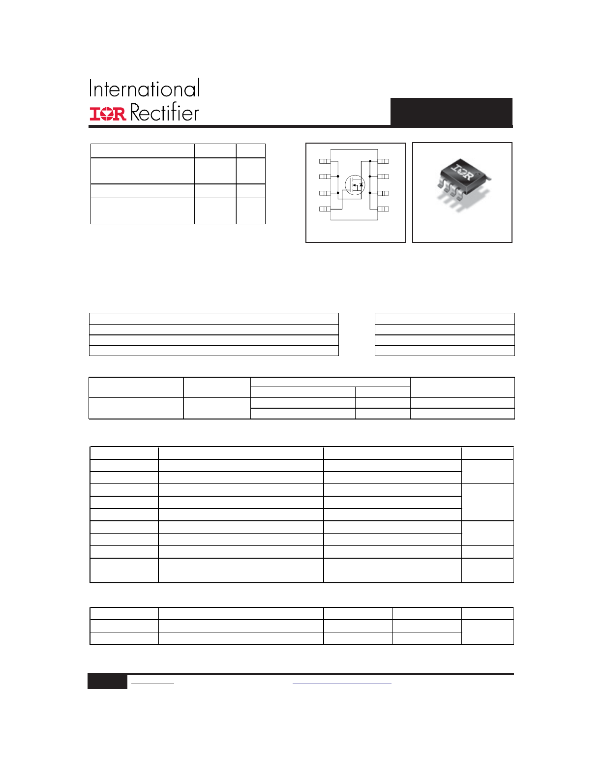
Top View
8
1
2
3
4
5
6
7
D
D
D
D
G
S
A
S
S
A
SO-8
Absolute Maximum Ratings
Parameter
Units
V
DS
Drain-to-Source Voltage
V
V
GS
Gate-to-Source Voltage
I
D
@ T
A
= 25°C
Continuous Drain Current, V
GS
@ 10V
I
D
@ T
A
= 70°C
Continuous Drain Current, V
GS
@ 10V
A
I
DM
Pulsed Drain Current
c
P
D
@T
A
= 25°C
Power Dissipation
W
P
D
@T
A
= 70°C
Power Dissipation
Linear Derating Factor
W/°C
T
J
Operating Junction and
°C
T
STG
Storage Temperature Range
Thermal Resistance
Parameter
Typ.
Max.
Units
R
θJL
Junction-to-Drain Lead
–––
20
°C/W
R
θJA
Junction-to-Ambient f
–––
50
-55 to + 155
2.5
0.02
1.6
Max.
20
16
160
± 20
30
IRF7832PbF-1
Form
Quantity
Tube/Bulk
95
IRF7832PbF-1
Tape and Reel
4000
IRF7832TRPbF-1
Package Type
Standard Pack
Orderable Part Number
IRF7832PbF-1
SO-8
Base Part Number
Features
Benefits
Industry-standard pinout SO-8 Package
⇒
Multi-Vendor Compatibility
Compatible with Existing Surface Mount Techniques
Easier Manufacturing
RoHS Compliant, Halogen-Free
Environmentally Friendlier
MSL1, Industrial qualification
Increased Reliability
V
DS
30
V
R
DS(on) max
(@V
GS
= 10V)
4.0
Q
g (typical)
34
nC
I
D
(@T
A
= 25°C)
20
A
mΩ
1
www.irf.com
©
2013 International Rectifier
Submit Datasheet Feedback
November 22, 2013
IRF7832PbF-1
2
www.irf.com
©
2013 International Rectifier
Submit Datasheet Feedback
November 22, 2013
S
D
G
Static @ T
J
= 25°C (unless otherwise specified)
Parameter
Min. Typ. Max. Units
BV
DSS
Drain-to-Source Breakdown Voltage
30
–––
–––
V
ΔΒV
DSS
/
ΔT
J
Breakdown Voltage Temp. Coefficient
–––
0.023
–––
V/°C
R
DS(on)
Static Drain-to-Source On-Resistance
–––
3.1
4.0
m
Ω
–––
3.7
4.8
V
GS(th)
Gate Threshold Voltage
1.39
–––
2.32
V
ΔV
GS(th)
Gate Threshold Voltage Coefficient
–––
5.7
––– mV/°C
I
DSS
Drain-to-Source Leakage Current
–––
–––
1.0
μA
–––
–––
150
I
GSS
Gate-to-Source Forward Leakage
–––
–––
100
nA
Gate-to-Source Reverse Leakage
–––
–––
-100
gfs
Forward Transconductance
77
–––
–––
S
Q
g
Total Gate Charge
–––
34
51
Q
gs1
Pre-Vth Gate-to-Source Charge
–––
8.6
–––
Q
gs2
Post-Vth Gate-to-Source Charge
–––
2.9
–––
nC
Q
gd
Gate-to-Drain Charge
–––
12
–––
Q
godr
Gate Charge Overdrive
–––
10.5
–––
See Fig. 16
Q
sw
Switch Charge (Q
gs2
+ Q
gd
)
–––
14.9
–––
Q
oss
Output Charge
–––
23
–––
nC
R
g
Gate Resistance
–––
1.2
2.4
Ω
t
d(on)
Turn-On Delay Time
–––
12
–––
t
r
Rise Time
–––
6.7
–––
t
d(off)
Turn-Off Delay Time
–––
21
–––
ns
t
f
Fall Time
–––
13
–––
C
iss
Input Capacitance
–––
4310
–––
C
oss
Output Capacitance
–––
990
–––
pF
C
rss
Reverse Transfer Capacitance
–––
450
–––
Avalanche Characteristics
Parameter
Units
E
AS
Single Pulse Avalanche Energy
d
mJ
I
AR
Avalanche Current
c
A
Diode Characteristics
Parameter
Min. Typ. Max. Units
I
S
Continuous Source Current
–––
–––
3.1
(Body Diode)
A
I
SM
Pulsed Source Current
–––
–––
160
(Body Diode)
c
V
SD
Diode Forward Voltage
–––
–––
1.0
V
t
rr
Reverse Recovery Time
–––
41
62
ns
Q
rr
Reverse Recovery Charge
–––
39
59
nC
t
on
Forward Turn-On Time
Intrinsic turn-on time is negligible (turn-on is dominated by LS+LD)
–––
I
D
= 16A
V
GS
= 0V
V
DS
= 15V
V
GS
= 4.5V, I
D
= 16A
e
V
GS
= 4.5V
Typ.
–––
V
DS
= V
GS
, I
D
= 250μA
Clamped Inductive Load
V
DS
= 15V, I
D
= 16A
V
DS
= 24V, V
GS
= 0V, T
J
= 125°C
T
J
= 25°C, I
F
= 16A, V
DD
= 10V
di/dt = 100A/μs
e
T
J
= 25°C, I
S
= 16A, V
GS
= 0V
e
showing the
integral reverse
p-n junction diode.
MOSFET symbol
V
DS
= 16V, V
GS
= 0V
V
DD
= 15V, V
GS
= 4.5V
I
D
= 16A
V
DS
= 15V
V
GS
= 20V
V
GS
= -20V
V
DS
= 24V, V
GS
= 0V
Conditions
V
GS
= 0V, I
D
= 250μA
Reference to 25°C, I
D
= 1mA
V
GS
= 10V, I
D
= 20A
e
Conditions
Max.
260
16
ƒ = 1.0MHz
IRF7832PbF-1
3
www.irf.com
©
2013 International Rectifier
Submit Datasheet Feedback
November 22, 2013
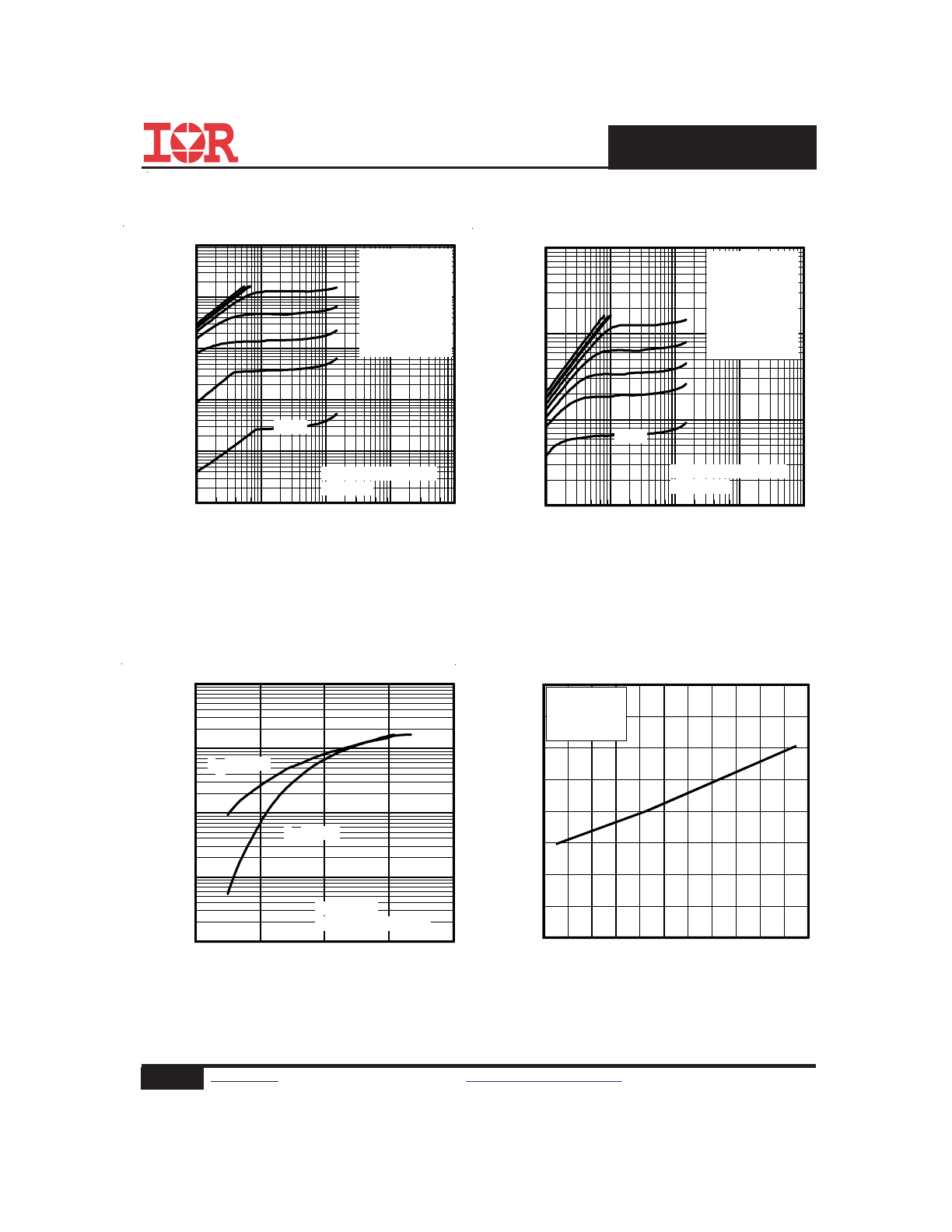
Fig 4. Normalized On-Resistance
Vs. Temperature
Fig 2. Typical Output Characteristics
Fig 1. Typical Output Characteristics
Fig 3. Typical Transfer Characteristics
0.1
1
10
100
1000
VDS, Drain-to-Source Voltage (V)
0.01
0.1
1
10
100
1000
I D
, D
ra
in
-t
o-
S
ou
rc
e
C
ur
re
nt
(
A
)
2.25V
20μs PULSE WIDTH
Tj = 25°C
VGS
TOP
10V
5.0V
4.5V
3.5V
3.0V
2.7V
2.5V
BOTTOM
2.25V
2.0
2.5
3.0
3.5
4.0
VGS, Gate-to-Source Voltage (V)
0
1
10
100
1000
I D
, D
ra
in
-t
o-
S
ou
rc
e
C
ur
re
nt
(
Α
)
TJ = 25°C
TJ = 150°C
VDS = 15V
20μs PULSE WIDTH
0.1
1
10
100
1000
VDS, Drain-to-Source Voltage (V)
1
10
100
1000
I D
, D
ra
in
-t
o-
S
ou
rc
e
C
ur
re
nt
(
A
)
2.25V
20μs PULSE WIDTH
Tj = 150°C
VGS
TOP
10V
5.0V
4.5V
3.5V
3.0V
2.7V
2.5V
BOTTOM
2.25V
-60 -40 -20
0
20 40 60 80 100 120 140 160
TJ, Junction Temperature (°C )
0.0
0.5
1.0
1.5
2.0
R
D
S
(o
n)
,
D
ra
in
-t
o
-S
ou
rc
e
O
n
R
es
is
ta
nc
e
(N
or
m
al
iz
ed
)
ID = 16A
VGS = 4.5V
IRF7832PbF-1
4
www.irf.com
©
2013 International Rectifier
Submit Datasheet Feedback
November 22, 2013
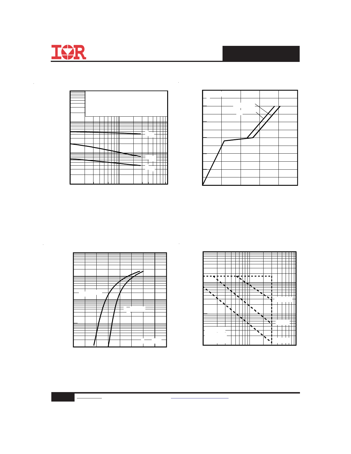
Fig 8. Maximum Safe Operating Area
Fig 6. Typical Gate Charge Vs.
Gate-to-Source Voltage
Fig 5. Typical Capacitance Vs.
Drain-to-Source Voltage
Fig 7. Typical Source-Drain Diode
Forward Voltage
1
10
100
VDS, Drain-to-Source Voltage (V)
100
1000
10000
100000
C
, C
ap
ac
ita
nc
e(
pF
)
VGS = 0V, f = 1 MHZ
Ciss = Cgs + Cgd, Cds SHORTED
Crss = Cgd
Coss = Cds + Cgd
Coss
Crss
Ciss
0
10
20
30
40
50
QG Total Gate Charge (nC)
0
1
2
3
4
5
6
V
G
S
, G
at
e-
to
-S
ou
rc
e
V
ol
ta
ge
(
V
)
VDS= 24V
VDS= 15V
ID= 16A
0.0 0.2
0.4
0.6 0.8
1.0 1.2
1.4
1.6
VSD , Source-to-Drain Voltage (V)
0.1
1
10
100
1000
I S
D
,
R
ev
er
se
D
ra
in
C
ur
re
nt
(
Α
)
VGS = 0V
TJ = 150°C
TJ = 25°C
1
10
100
VDS, Drain-to-Source Voltage (V)
1
10
100
1000
I D
,
D
ra
in
-t
o-
S
ou
rc
e
C
ur
re
nt
(
A
)
Tc = 25°C
Tj = 150°C
Single Pulse
1msec
10msec
100μsec
IRF7832PbF-1
5
www.irf.com
©
2013 International Rectifier
Submit Datasheet Feedback
November 22, 2013
Fig 11. Maximum Effective Transient Thermal Impedance, Junction-to-Ambient
Fig 9. Maximum Drain Current Vs.
Case Temperature
Fig 10. Threshold Voltage Vs. Temperature
25
50
75
100
125
150
TC , Case Temperature (°C)
0
4
8
12
16
20
24
I D
,
D
ra
in
C
ur
re
nt
(
A
)
1E-006
1E-005
0.0001
0.001
0.01
0.1
1
10
100
t1 , Rectangular Pulse Duration (sec)
0.01
0.1
1
10
100
T
he
rm
al
R
es
po
ns
e
(
Z
th
JA
)
0.20
0.10
D = 0.50
0.02
0.01
0.05
SINGLE PULSE
( THERMAL RESPONSE )
-60 -40 -20
0
20 40 60 80 100 120 140 160
TJ , Temperature (°C)
0.5
1.0
1.5
2.0
2.5
V
G
S
(t
h)
, G
at
e
T
hr
es
ho
ld
V
ol
ta
ge
(
V
)
ID = 250μA
IRF7832PbF-1
6
www.irf.com
©
2013 International Rectifier
Submit Datasheet Feedback
November 22, 2013
Fig 13. Maximum Avalanche Energy
vs. Drain Current
25
50
75
100
125
150
Starting TJ , Junction Temperature (°C)
0
100
200
300
400
500
600
E
A
S
,
S
in
gl
e
P
ul
se
A
va
la
nc
he
E
ne
rg
y
(m
J)
ID
TOP 7.0A
13A
BOTTOM 16A
Fig 16. Switching Time Test Circuit
Fig 17. Switching Time Waveforms
Fig 12. On-Resistance vs. Gate Voltage
D.U.T.
V
DS
I
D
I
G
3mA
V
GS
.3
μF
50K
Ω
.2
μF
12V
Current Regulator
Same Type as D.U.T.
Current Sampling Resistors
+
-
Fig 15. Gate Charge Test Circuit
Fig 14. Unclamped Inductive Test Circuit
and Waveform
tp
V
(BR)DSS
I
AS
RG
IAS
0.01
Ω
tp
D.U.T
L
VDS
+
- VDD
DRIVER
A
15V
20V
VGS
V
GS
Pulse Width < 1μs
Duty Factor < 0.1%
V
DD
V
DS
L
D
D.U.T
+
-
V
GS
V
DS
90%
10%
t
d(on)
t
d(off)
t
r
t
f
2
3
4
5
6
7
8
9
10
VGS, Gate -to -Source Voltage (V)
0
2
4
6
8
10
R
D
S
(o
n)
,
D
ra
in
-t
o
-S
ou
rc
e
O
n
R
es
is
ta
nc
e
(m
Ω
)
ID = 20A
TJ = 125°C
TJ = 25°C
IRF7832PbF-1
7
www.irf.com
©
2013 International Rectifier
Submit Datasheet Feedback
November 22, 2013
Fig 18.
Peak Diode Recovery dv/dt Test Circuit for N-Channel
HEXFET
®
Power MOSFETs
Circuit Layout Considerations
• Low Stray Inductance
• Ground Plane
• Low Leakage Inductance
Current Transformer
P.W.
Period
di/dt
Diode Recovery
dv/dt
Ripple
≤ 5%
Body Diode Forward Drop
Re-Applied
Voltage
Reverse
Recovery
Current
Body Diode Forward
Current
V
GS
=10V
V
DD
I
SD
Driver Gate Drive
D.U.T. I
SD
Waveform
D.U.T. V
DS
Waveform
Inductor Curent
D =
P.W.
Period
*
V
GS
= 5V for Logic Level Devices
*
+
-
+
+
+
-
-
-
R
G
V
DD
• dv/dt controlled by R
G
• Driver same type as D.U.T.
• I
SD
controlled by Duty Factor "D"
• D.U.T. - Device Under Test
D.U.T
Fig 19. Gate Charge Waveform
Vds
Vgs
Id
Vgs(th)
Qgs1 Qgs2
Qgd
Qgodr
IRF7832PbF-1
8
www.irf.com
©
2013 International Rectifier
Submit Datasheet Feedback
November 22, 2013
Control FET
Special attention has been given to the power losses
in the switching elements of the circuit - Q1 and Q2.
Power losses in the high side switch Q1, also called
the Control FET, are impacted by the R
ds(on)
of the
MOSFET, but these conduction losses are only about
one half of the total losses.
Power losses in the control switch Q1 are given
by;
P
loss
= P
conduction
+ P
switching
+ P
drive
+ P
output
This can be expanded and approximated by;
P
loss
= I
rms
2
× R
ds(on )
(
)
+ I ×
Q
gd
i
g
× V
in
× f
⎛
⎝
⎜
⎞
⎠
⎟ + I ×
Q
gs 2
i
g
× V
in
× f
⎛
⎝
⎜
⎞
⎠
⎟
+ Q
g
× V
g
× f
(
)
+
Q
oss
2
×V
in
× f
⎛
⎝
⎞
⎠
This simplified loss equation includes the terms Q
gs2
and Q
oss
which are new to Power MOSFET data sheets.
Q
gs2
is a sub element of traditional gate-source
charge that is included in all MOSFET data sheets.
The importance of splitting this gate-source charge
into two sub elements, Q
gs1
and Q
gs2
, can be seen from
Fig 16.
Q
gs2
indicates the charge that must be supplied by
the gate driver between the time that the threshold
voltage has been reached and the time the drain cur-
rent rises to I
dmax
at which time the drain voltage be-
gins to change. Minimizing Q
gs2
is a critical factor in
reducing switching losses in Q1.
Q
oss
is the charge that must be supplied to the out-
put capacitance of the MOSFET during every switch-
ing cycle. Figure A shows how Q
oss
is formed by the
parallel combination of the voltage dependant (non-
linear) capacitances C
ds
and C
dg
when multiplied by
the power supply input buss voltage.
Synchronous FET
The power loss equation for Q2 is approximated
by;
P
loss
= P
conduction
+ P
drive
+ P
output
*
P
loss
= I
rms
2
× R
ds(on)
(
)
+ Q
g
× V
g
× f
(
)
+
Q
oss
2
× V
in
× f
⎛
⎝
⎜
⎞
⎠
+ Q
rr
× V
in
× f
(
)
*dissipated primarily in Q1.
For the synchronous MOSFET Q2, R
ds(on)
is an im-
portant characteristic; however, once again the im-
portance of gate charge must not be overlooked since
it impacts three critical areas. Under light load the
MOSFET must still be turned on and off by the con-
trol IC so the gate drive losses become much more
significant. Secondly, the output charge Q
oss
and re-
verse recovery charge Q
rr
both generate losses that
are transfered to Q1 and increase the dissipation in
that device. Thirdly, gate charge will impact the
MOSFETs’ susceptibility to Cdv/dt turn on.
The drain of Q2 is connected to the switching node
of the converter and therefore sees transitions be-
tween ground and V
in
. As Q1 turns on and off there is
a rate of change of drain voltage dV/dt which is ca-
pacitively coupled to the gate of Q2 and can induce
a voltage spike on the gate that is sufficient to turn
the MOSFET on, resulting in shoot-through current .
The ratio of Q
gd
/Q
gs1
must be minimized to reduce the
potential for Cdv/dt turn on.
Power MOSFET Selection for Non-Isolated DC/DC Converters
Figure A: Q
oss
Characteristic
IRF7832PbF-1
9
www.irf.com
©
2013 International Rectifier
Submit Datasheet Feedback
November 22, 2013
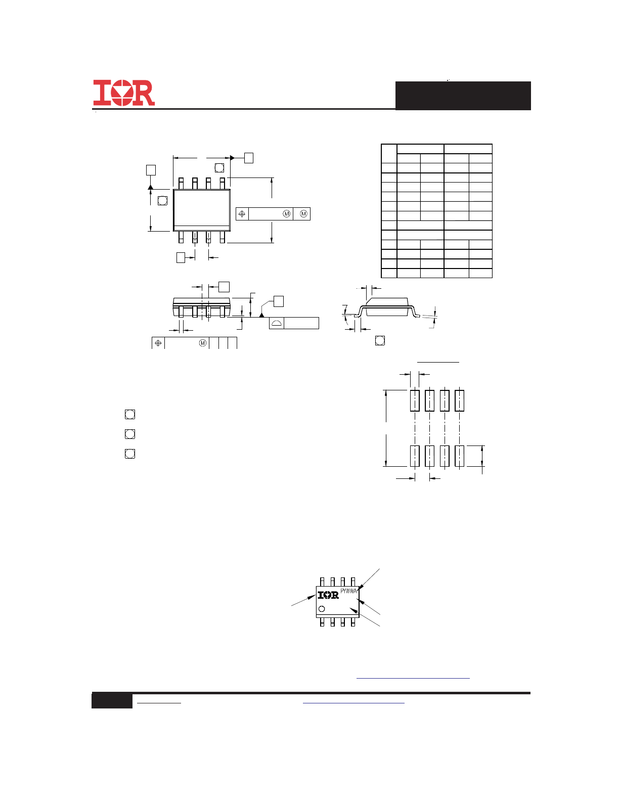
SO-8 Package Details
SO-8 Part Marking
e 1
D
E
y
b
A
A1
H
K
L
.189
.1497
0°
.013
.050 BASIC
.0532
.0040
.2284
.0099
.016
.1968
.1574
8°
.020
.0688
.0098
.2440
.0196
.050
4.80
3.80
0.33
1.35
0.10
5.80
0.25
0.40
0°
1.27 BASIC
5.00
4.00
0.51
1.75
0.25
6.20
0.50
1.27
MIN
MAX
MILLIMETERS
INCHES
MIN
MAX
DIM
8°
e
c
.0075
.0098
0.19
0.25
.025 BASIC
0.635 BASIC
8
7
5
6
5
D
B
E
A
e
6X
H
0.25 [.010]
A
6
7
K x 45°
8X L
8X c
y
0.25 [.010]
C A B
e1
A
A1
8X b
C
0.10 [.004]
4
3
1
2
FOOTPRINT
8X 0.72 [.028]
6.46 [.255]
3X 1.27 [.050]
4. OUTLINE CONFORMS TO JEDEC OUTLINE MS-012AA.
NOT ES:
1. DIMENSIONING & TOLERANCING PER ASME Y14.5M-1994.
2. CONT ROLLING DIMENSION: MILLIMET ER
3. DIMENSIONS ARE SHOWN IN MILLIMETERS [INCHES].
5 DIMENSION DOES NOT INCLUDE MOLD PROT RUSIONS.
6 DIMENSION DOES NOT INCLUDE MOLD PROT RUSIONS.
MOLD PROTRUSIONS NOT TO EXCEED 0.25 [.010].
7 DIMENSION IS T HE LENGT H OF LEAD FOR SOLDERING TO
A SUBST RAT E.
MOLD PROTRUSIONS NOT TO EXCEED 0.15 [.006].
8X 1.78 [.070]
P = DISGNATES LEAD - FREE
EXAMPLE: THIS IS AN IRF7101 (MOSFET)
F7101
XXXX
INTERNATIONAL
LOGO
RECTIFIER
PART NUMBER
LOT CODE
PRODUCT (OPTIONAL)
DATE CODE (YWW)
Y = LAST DIGIT OF THE YEAR
WW = WEEK
A = ASSEMBLY SITE CODE
Note: For the most current drawing please refer to IR website at
http://www.irf.com/package/
IRF7832PbF-1
10
www.irf.com
©
2013 International Rectifier
Submit Datasheet Feedback
November 22, 2013
Notes:
Repetitive rating; pulse width limited by max. junction temperature.
Starting T
J
= 25°C, L = 2.0mH, R
G
= 25
Ω, I
AS
= 16A.
Pulse width ≤ 400μs; duty cycle ≤ 2%.
When mounted on 1 inch square copper board.
330.00
(12.992)
MAX.
14.40 ( .566 )
12.40 ( .488 )
NOTES :
1. CONTROLLING DIMENSION : MILLIMETER.
2. OUTLINE CONFORMS TO EIA-481 & EIA-541.
FEED DIRECTION
TERMINAL NUMBER 1
12.3 ( .484 )
11.7 ( .461 )
8.1 ( .318 )
7.9 ( .312 )
NOTES:
1. CONTROLLING DIMENSION : MILLIMETER.
2. ALL DIMENSIONS ARE SHOWN IN MILLIMETERS(INCHES).
3. OUTLINE CONFORMS TO EIA-481 & EIA-541.
SO-8 Tape and Reel
Note: For the most current drawing please refer to IR website at
http://www.irf.com/package/
† Qualification standards can be found at International Rectifier’s web site:
http://www.irf.com/product-info/reliability
††
Applicable version of JEDEC standard at the time of product release
MS L1
(per JEDEC J-S TD-020D
††
)
RoHS compliant
Yes
Qualification information
†
Qualification level
Industrial
(per JEDEC JES D47F
††
guidelines)
Moisture Sensitivity Level
SO-8
IR WORLD HEADQUARTERS: 101 N. Sepulveda Blvd., El Segundo, California 90245, USA
To contact International Rectifier, please visit
http://www.irf.com/whoto-call/
HEXFET
®
Power MOSFET
Notes
through
are on page 10
Applications
l
Synchronous MOSFET for Notebook Processor Power
l
Synchronous Rectifier MOSFET for Isolated DC-DC Converters in Networking Systems
Top View
8
1
2
3
4
5
6
7
D
D
D
D
G
S
A
S
S
A
SO-8
Absolute Maximum Ratings
Parameter
Units
V
DS
Drain-to-Source Voltage
V
V
GS
Gate-to-Source Voltage
I
D
@ T
A
= 25°C
Continuous Drain Current, V
GS
@ 10V
I
D
@ T
A
= 70°C
Continuous Drain Current, V
GS
@ 10V
A
I
DM
Pulsed Drain Current
c
P
D
@T
A
= 25°C
Power Dissipation
W
P
D
@T
A
= 70°C
Power Dissipation
Linear Derating Factor
W/°C
T
J
Operating Junction and
°C
T
STG
Storage Temperature Range
Thermal Resistance
Parameter
Typ.
Max.
Units
R
θJL
Junction-to-Drain Lead
–––
20
°C/W
R
θJA
Junction-to-Ambient f
–––
50
-55 to + 155
2.5
0.02
1.6
Max.
20
16
160
± 20
30
IRF7832PbF-1
Form
Quantity
Tube/Bulk
95
IRF7832PbF-1
Tape and Reel
4000
IRF7832TRPbF-1
Package Type
Standard Pack
Orderable Part Number
IRF7832PbF-1
SO-8
Base Part Number
Features
Benefits
Industry-standard pinout SO-8 Package
⇒
Multi-Vendor Compatibility
Compatible with Existing Surface Mount Techniques
Easier Manufacturing
RoHS Compliant, Halogen-Free
Environmentally Friendlier
MSL1, Industrial qualification
Increased Reliability
V
DS
30
V
R
DS(on) max
(@V
GS
= 10V)
4.0
Q
g (typical)
34
nC
I
D
(@T
A
= 25°C)
20
A
mΩ
1
www.irf.com
©
2013 International Rectifier
Submit Datasheet Feedback
November 22, 2013
IRF7832PbF-1
2
www.irf.com
©
2013 International Rectifier
Submit Datasheet Feedback
November 22, 2013
S
D
G
Static @ T
J
= 25°C (unless otherwise specified)
Parameter
Min. Typ. Max. Units
BV
DSS
Drain-to-Source Breakdown Voltage
30
–––
–––
V
ΔΒV
DSS
/
ΔT
J
Breakdown Voltage Temp. Coefficient
–––
0.023
–––
V/°C
R
DS(on)
Static Drain-to-Source On-Resistance
–––
3.1
4.0
m
Ω
–––
3.7
4.8
V
GS(th)
Gate Threshold Voltage
1.39
–––
2.32
V
ΔV
GS(th)
Gate Threshold Voltage Coefficient
–––
5.7
––– mV/°C
I
DSS
Drain-to-Source Leakage Current
–––
–––
1.0
μA
–––
–––
150
I
GSS
Gate-to-Source Forward Leakage
–––
–––
100
nA
Gate-to-Source Reverse Leakage
–––
–––
-100
gfs
Forward Transconductance
77
–––
–––
S
Q
g
Total Gate Charge
–––
34
51
Q
gs1
Pre-Vth Gate-to-Source Charge
–––
8.6
–––
Q
gs2
Post-Vth Gate-to-Source Charge
–––
2.9
–––
nC
Q
gd
Gate-to-Drain Charge
–––
12
–––
Q
godr
Gate Charge Overdrive
–––
10.5
–––
See Fig. 16
Q
sw
Switch Charge (Q
gs2
+ Q
gd
)
–––
14.9
–––
Q
oss
Output Charge
–––
23
–––
nC
R
g
Gate Resistance
–––
1.2
2.4
Ω
t
d(on)
Turn-On Delay Time
–––
12
–––
t
r
Rise Time
–––
6.7
–––
t
d(off)
Turn-Off Delay Time
–––
21
–––
ns
t
f
Fall Time
–––
13
–––
C
iss
Input Capacitance
–––
4310
–––
C
oss
Output Capacitance
–––
990
–––
pF
C
rss
Reverse Transfer Capacitance
–––
450
–––
Avalanche Characteristics
Parameter
Units
E
AS
Single Pulse Avalanche Energy
d
mJ
I
AR
Avalanche Current
c
A
Diode Characteristics
Parameter
Min. Typ. Max. Units
I
S
Continuous Source Current
–––
–––
3.1
(Body Diode)
A
I
SM
Pulsed Source Current
–––
–––
160
(Body Diode)
c
V
SD
Diode Forward Voltage
–––
–––
1.0
V
t
rr
Reverse Recovery Time
–––
41
62
ns
Q
rr
Reverse Recovery Charge
–––
39
59
nC
t
on
Forward Turn-On Time
Intrinsic turn-on time is negligible (turn-on is dominated by LS+LD)
–––
I
D
= 16A
V
GS
= 0V
V
DS
= 15V
V
GS
= 4.5V, I
D
= 16A
e
V
GS
= 4.5V
Typ.
–––
V
DS
= V
GS
, I
D
= 250μA
Clamped Inductive Load
V
DS
= 15V, I
D
= 16A
V
DS
= 24V, V
GS
= 0V, T
J
= 125°C
T
J
= 25°C, I
F
= 16A, V
DD
= 10V
di/dt = 100A/μs
e
T
J
= 25°C, I
S
= 16A, V
GS
= 0V
e
showing the
integral reverse
p-n junction diode.
MOSFET symbol
V
DS
= 16V, V
GS
= 0V
V
DD
= 15V, V
GS
= 4.5V
I
D
= 16A
V
DS
= 15V
V
GS
= 20V
V
GS
= -20V
V
DS
= 24V, V
GS
= 0V
Conditions
V
GS
= 0V, I
D
= 250μA
Reference to 25°C, I
D
= 1mA
V
GS
= 10V, I
D
= 20A
e
Conditions
Max.
260
16
ƒ = 1.0MHz
IRF7832PbF-1
3
www.irf.com
©
2013 International Rectifier
Submit Datasheet Feedback
November 22, 2013
Fig 4. Normalized On-Resistance
Vs. Temperature
Fig 2. Typical Output Characteristics
Fig 1. Typical Output Characteristics
Fig 3. Typical Transfer Characteristics
0.1
1
10
100
1000
VDS, Drain-to-Source Voltage (V)
0.01
0.1
1
10
100
1000
I D
, D
ra
in
-t
o-
S
ou
rc
e
C
ur
re
nt
(
A
)
2.25V
20μs PULSE WIDTH
Tj = 25°C
VGS
TOP
10V
5.0V
4.5V
3.5V
3.0V
2.7V
2.5V
BOTTOM
2.25V
2.0
2.5
3.0
3.5
4.0
VGS, Gate-to-Source Voltage (V)
0
1
10
100
1000
I D
, D
ra
in
-t
o-
S
ou
rc
e
C
ur
re
nt
(
Α
)
TJ = 25°C
TJ = 150°C
VDS = 15V
20μs PULSE WIDTH
0.1
1
10
100
1000
VDS, Drain-to-Source Voltage (V)
1
10
100
1000
I D
, D
ra
in
-t
o-
S
ou
rc
e
C
ur
re
nt
(
A
)
2.25V
20μs PULSE WIDTH
Tj = 150°C
VGS
TOP
10V
5.0V
4.5V
3.5V
3.0V
2.7V
2.5V
BOTTOM
2.25V
-60 -40 -20
0
20 40 60 80 100 120 140 160
TJ, Junction Temperature (°C )
0.0
0.5
1.0
1.5
2.0
R
D
S
(o
n)
,
D
ra
in
-t
o
-S
ou
rc
e
O
n
R
es
is
ta
nc
e
(N
or
m
al
iz
ed
)
ID = 16A
VGS = 4.5V
IRF7832PbF-1
4
www.irf.com
©
2013 International Rectifier
Submit Datasheet Feedback
November 22, 2013
Fig 8. Maximum Safe Operating Area
Fig 6. Typical Gate Charge Vs.
Gate-to-Source Voltage
Fig 5. Typical Capacitance Vs.
Drain-to-Source Voltage
Fig 7. Typical Source-Drain Diode
Forward Voltage
1
10
100
VDS, Drain-to-Source Voltage (V)
100
1000
10000
100000
C
, C
ap
ac
ita
nc
e(
pF
)
VGS = 0V, f = 1 MHZ
Ciss = Cgs + Cgd, Cds SHORTED
Crss = Cgd
Coss = Cds + Cgd
Coss
Crss
Ciss
0
10
20
30
40
50
QG Total Gate Charge (nC)
0
1
2
3
4
5
6
V
G
S
, G
at
e-
to
-S
ou
rc
e
V
ol
ta
ge
(
V
)
VDS= 24V
VDS= 15V
ID= 16A
0.0 0.2
0.4
0.6 0.8
1.0 1.2
1.4
1.6
VSD , Source-to-Drain Voltage (V)
0.1
1
10
100
1000
I S
D
,
R
ev
er
se
D
ra
in
C
ur
re
nt
(
Α
)
VGS = 0V
TJ = 150°C
TJ = 25°C
1
10
100
VDS, Drain-to-Source Voltage (V)
1
10
100
1000
I D
,
D
ra
in
-t
o-
S
ou
rc
e
C
ur
re
nt
(
A
)
Tc = 25°C
Tj = 150°C
Single Pulse
1msec
10msec
100μsec
IRF7832PbF-1
5
www.irf.com
©
2013 International Rectifier
Submit Datasheet Feedback
November 22, 2013
Fig 11. Maximum Effective Transient Thermal Impedance, Junction-to-Ambient
Fig 9. Maximum Drain Current Vs.
Case Temperature
Fig 10. Threshold Voltage Vs. Temperature
25
50
75
100
125
150
TC , Case Temperature (°C)
0
4
8
12
16
20
24
I D
,
D
ra
in
C
ur
re
nt
(
A
)
1E-006
1E-005
0.0001
0.001
0.01
0.1
1
10
100
t1 , Rectangular Pulse Duration (sec)
0.01
0.1
1
10
100
T
he
rm
al
R
es
po
ns
e
(
Z
th
JA
)
0.20
0.10
D = 0.50
0.02
0.01
0.05
SINGLE PULSE
( THERMAL RESPONSE )
-60 -40 -20
0
20 40 60 80 100 120 140 160
TJ , Temperature (°C)
0.5
1.0
1.5
2.0
2.5
V
G
S
(t
h)
, G
at
e
T
hr
es
ho
ld
V
ol
ta
ge
(
V
)
ID = 250μA
IRF7832PbF-1
6
www.irf.com
©
2013 International Rectifier
Submit Datasheet Feedback
November 22, 2013
Fig 13. Maximum Avalanche Energy
vs. Drain Current
25
50
75
100
125
150
Starting TJ , Junction Temperature (°C)
0
100
200
300
400
500
600
E
A
S
,
S
in
gl
e
P
ul
se
A
va
la
nc
he
E
ne
rg
y
(m
J)
ID
TOP 7.0A
13A
BOTTOM 16A
Fig 16. Switching Time Test Circuit
Fig 17. Switching Time Waveforms
Fig 12. On-Resistance vs. Gate Voltage
D.U.T.
V
DS
I
D
I
G
3mA
V
GS
.3
μF
50K
Ω
.2
μF
12V
Current Regulator
Same Type as D.U.T.
Current Sampling Resistors
+
-
Fig 15. Gate Charge Test Circuit
Fig 14. Unclamped Inductive Test Circuit
and Waveform
tp
V
(BR)DSS
I
AS
RG
IAS
0.01
Ω
tp
D.U.T
L
VDS
+
- VDD
DRIVER
A
15V
20V
VGS
V
GS
Pulse Width < 1μs
Duty Factor < 0.1%
V
DD
V
DS
L
D
D.U.T
+
-
V
GS
V
DS
90%
10%
t
d(on)
t
d(off)
t
r
t
f
2
3
4
5
6
7
8
9
10
VGS, Gate -to -Source Voltage (V)
0
2
4
6
8
10
R
D
S
(o
n)
,
D
ra
in
-t
o
-S
ou
rc
e
O
n
R
es
is
ta
nc
e
(m
Ω
)
ID = 20A
TJ = 125°C
TJ = 25°C
IRF7832PbF-1
7
www.irf.com
©
2013 International Rectifier
Submit Datasheet Feedback
November 22, 2013
Fig 18.
Peak Diode Recovery dv/dt Test Circuit for N-Channel
HEXFET
®
Power MOSFETs
Circuit Layout Considerations
• Low Stray Inductance
• Ground Plane
• Low Leakage Inductance
Current Transformer
P.W.
Period
di/dt
Diode Recovery
dv/dt
Ripple
≤ 5%
Body Diode Forward Drop
Re-Applied
Voltage
Reverse
Recovery
Current
Body Diode Forward
Current
V
GS
=10V
V
DD
I
SD
Driver Gate Drive
D.U.T. I
SD
Waveform
D.U.T. V
DS
Waveform
Inductor Curent
D =
P.W.
Period
*
V
GS
= 5V for Logic Level Devices
*
+
-
+
+
+
-
-
-
R
G
V
DD
• dv/dt controlled by R
G
• Driver same type as D.U.T.
• I
SD
controlled by Duty Factor "D"
• D.U.T. - Device Under Test
D.U.T
Fig 19. Gate Charge Waveform
Vds
Vgs
Id
Vgs(th)
Qgs1 Qgs2
Qgd
Qgodr
IRF7832PbF-1
8
www.irf.com
©
2013 International Rectifier
Submit Datasheet Feedback
November 22, 2013
Control FET
Special attention has been given to the power losses
in the switching elements of the circuit - Q1 and Q2.
Power losses in the high side switch Q1, also called
the Control FET, are impacted by the R
ds(on)
of the
MOSFET, but these conduction losses are only about
one half of the total losses.
Power losses in the control switch Q1 are given
by;
P
loss
= P
conduction
+ P
switching
+ P
drive
+ P
output
This can be expanded and approximated by;
P
loss
= I
rms
2
× R
ds(on )
(
)
+ I ×
Q
gd
i
g
× V
in
× f
⎛
⎝
⎜
⎞
⎠
⎟ + I ×
Q
gs 2
i
g
× V
in
× f
⎛
⎝
⎜
⎞
⎠
⎟
+ Q
g
× V
g
× f
(
)
+
Q
oss
2
×V
in
× f
⎛
⎝
⎞
⎠
This simplified loss equation includes the terms Q
gs2
and Q
oss
which are new to Power MOSFET data sheets.
Q
gs2
is a sub element of traditional gate-source
charge that is included in all MOSFET data sheets.
The importance of splitting this gate-source charge
into two sub elements, Q
gs1
and Q
gs2
, can be seen from
Fig 16.
Q
gs2
indicates the charge that must be supplied by
the gate driver between the time that the threshold
voltage has been reached and the time the drain cur-
rent rises to I
dmax
at which time the drain voltage be-
gins to change. Minimizing Q
gs2
is a critical factor in
reducing switching losses in Q1.
Q
oss
is the charge that must be supplied to the out-
put capacitance of the MOSFET during every switch-
ing cycle. Figure A shows how Q
oss
is formed by the
parallel combination of the voltage dependant (non-
linear) capacitances C
ds
and C
dg
when multiplied by
the power supply input buss voltage.
Synchronous FET
The power loss equation for Q2 is approximated
by;
P
loss
= P
conduction
+ P
drive
+ P
output
*
P
loss
= I
rms
2
× R
ds(on)
(
)
+ Q
g
× V
g
× f
(
)
+
Q
oss
2
× V
in
× f
⎛
⎝
⎜
⎞
⎠
+ Q
rr
× V
in
× f
(
)
*dissipated primarily in Q1.
For the synchronous MOSFET Q2, R
ds(on)
is an im-
portant characteristic; however, once again the im-
portance of gate charge must not be overlooked since
it impacts three critical areas. Under light load the
MOSFET must still be turned on and off by the con-
trol IC so the gate drive losses become much more
significant. Secondly, the output charge Q
oss
and re-
verse recovery charge Q
rr
both generate losses that
are transfered to Q1 and increase the dissipation in
that device. Thirdly, gate charge will impact the
MOSFETs’ susceptibility to Cdv/dt turn on.
The drain of Q2 is connected to the switching node
of the converter and therefore sees transitions be-
tween ground and V
in
. As Q1 turns on and off there is
a rate of change of drain voltage dV/dt which is ca-
pacitively coupled to the gate of Q2 and can induce
a voltage spike on the gate that is sufficient to turn
the MOSFET on, resulting in shoot-through current .
The ratio of Q
gd
/Q
gs1
must be minimized to reduce the
potential for Cdv/dt turn on.
Power MOSFET Selection for Non-Isolated DC/DC Converters
Figure A: Q
oss
Characteristic
IRF7832PbF-1
9
www.irf.com
©
2013 International Rectifier
Submit Datasheet Feedback
November 22, 2013
SO-8 Package Details
SO-8 Part Marking
e 1
D
E
y
b
A
A1
H
K
L
.189
.1497
0°
.013
.050 BASIC
.0532
.0040
.2284
.0099
.016
.1968
.1574
8°
.020
.0688
.0098
.2440
.0196
.050
4.80
3.80
0.33
1.35
0.10
5.80
0.25
0.40
0°
1.27 BASIC
5.00
4.00
0.51
1.75
0.25
6.20
0.50
1.27
MIN
MAX
MILLIMETERS
INCHES
MIN
MAX
DIM
8°
e
c
.0075
.0098
0.19
0.25
.025 BASIC
0.635 BASIC
8
7
5
6
5
D
B
E
A
e
6X
H
0.25 [.010]
A
6
7
K x 45°
8X L
8X c
y
0.25 [.010]
C A B
e1
A
A1
8X b
C
0.10 [.004]
4
3
1
2
FOOTPRINT
8X 0.72 [.028]
6.46 [.255]
3X 1.27 [.050]
4. OUTLINE CONFORMS TO JEDEC OUTLINE MS-012AA.
NOT ES:
1. DIMENSIONING & TOLERANCING PER ASME Y14.5M-1994.
2. CONT ROLLING DIMENSION: MILLIMET ER
3. DIMENSIONS ARE SHOWN IN MILLIMETERS [INCHES].
5 DIMENSION DOES NOT INCLUDE MOLD PROT RUSIONS.
6 DIMENSION DOES NOT INCLUDE MOLD PROT RUSIONS.
MOLD PROTRUSIONS NOT TO EXCEED 0.25 [.010].
7 DIMENSION IS T HE LENGT H OF LEAD FOR SOLDERING TO
A SUBST RAT E.
MOLD PROTRUSIONS NOT TO EXCEED 0.15 [.006].
8X 1.78 [.070]
P = DISGNATES LEAD - FREE
EXAMPLE: THIS IS AN IRF7101 (MOSFET)
F7101
XXXX
INTERNATIONAL
LOGO
RECTIFIER
PART NUMBER
LOT CODE
PRODUCT (OPTIONAL)
DATE CODE (YWW)
Y = LAST DIGIT OF THE YEAR
WW = WEEK
A = ASSEMBLY SITE CODE
Note: For the most current drawing please refer to IR website at
http://www.irf.com/package/
IRF7832PbF-1
10
www.irf.com
©
2013 International Rectifier
Submit Datasheet Feedback
November 22, 2013
Notes:
Repetitive rating; pulse width limited by max. junction temperature.
Starting T
J
= 25°C, L = 2.0mH, R
G
= 25
Ω, I
AS
= 16A.
Pulse width ≤ 400μs; duty cycle ≤ 2%.
When mounted on 1 inch square copper board.
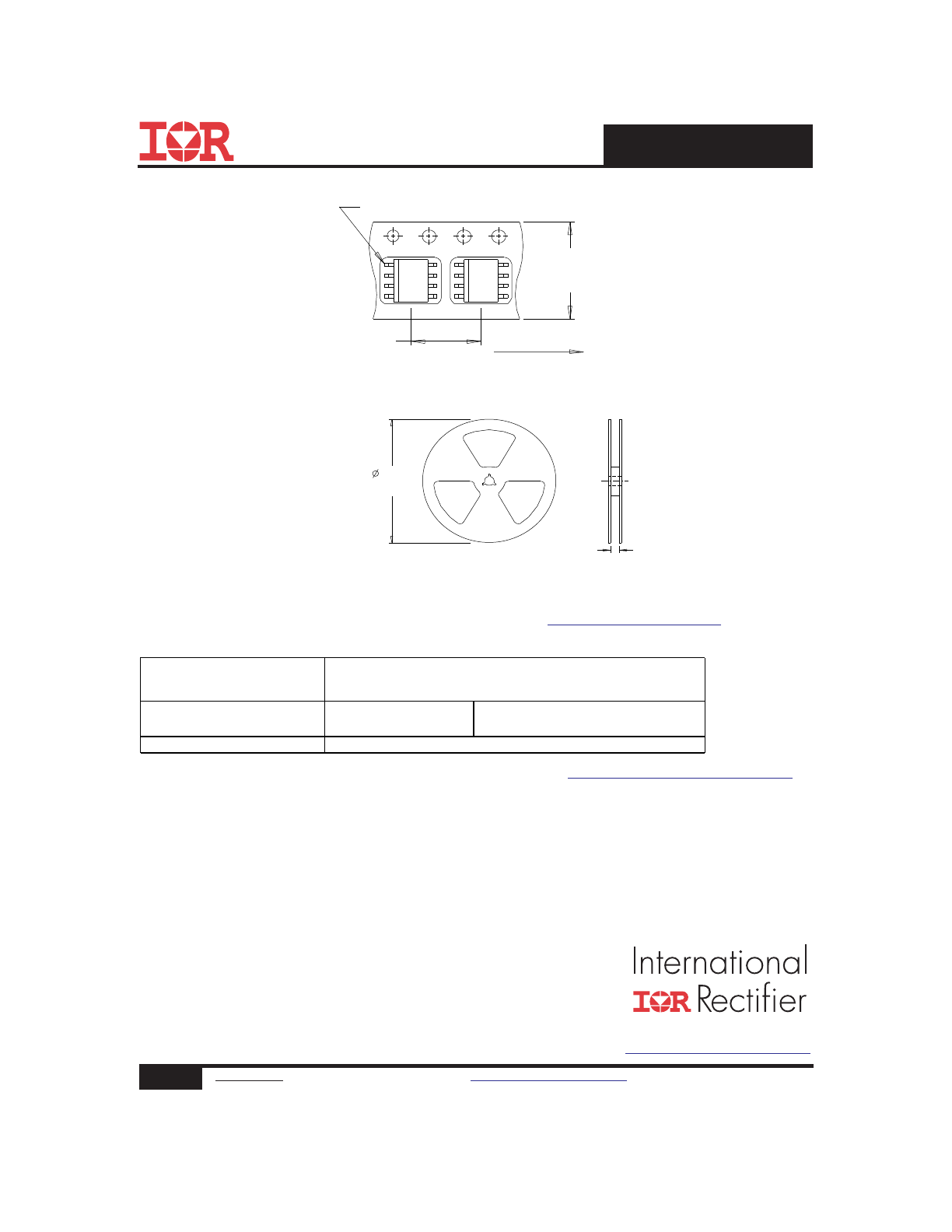
330.00
(12.992)
MAX.
14.40 ( .566 )
12.40 ( .488 )
NOTES :
1. CONTROLLING DIMENSION : MILLIMETER.
2. OUTLINE CONFORMS TO EIA-481 & EIA-541.
FEED DIRECTION
TERMINAL NUMBER 1
12.3 ( .484 )
11.7 ( .461 )
8.1 ( .318 )
7.9 ( .312 )
NOTES:
1. CONTROLLING DIMENSION : MILLIMETER.
2. ALL DIMENSIONS ARE SHOWN IN MILLIMETERS(INCHES).
3. OUTLINE CONFORMS TO EIA-481 & EIA-541.
SO-8 Tape and Reel
Note: For the most current drawing please refer to IR website at
http://www.irf.com/package/
† Qualification standards can be found at International Rectifier’s web site:
http://www.irf.com/product-info/reliability
††
Applicable version of JEDEC standard at the time of product release
MS L1
(per JEDEC J-S TD-020D
††
)
RoHS compliant
Yes
Qualification information
†
Qualification level
Industrial
(per JEDEC JES D47F
††
guidelines)
Moisture Sensitivity Level
SO-8
IR WORLD HEADQUARTERS: 101 N. Sepulveda Blvd., El Segundo, California 90245, USA
To contact International Rectifier, please visit
http://www.irf.com/whoto-call/