
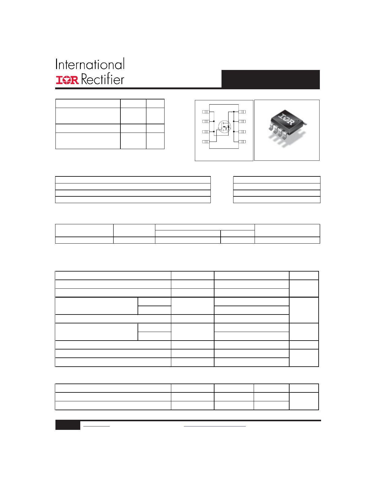
SO-8
Absolute Maximum Ratings
Symbol
Units
V
DS
V
GS
Continuous Drain or Source
T
A
= 25°C
(V
GS
≥ 4.5V)
T
A
= 70°C
I
DM
T
A
= 25°C
T
A
= 70°C
T
J
, T
STG
°C
I
S
I
SM
Thermal Resistance
Symbol
Typ
Max
Units
R
θJA
–––
50
R
θJL
–––
20
A
W
A
°C/W
Parameter
Maximum Junction-to-Ambient
eh
Maximum Junction-to-Lead
h
Junction & Storage Temperature Range
Continuous Source Current (Body Diode)
Pulsed Source Current
c
Parameter
V
Power Dissipation
e
Drain-Source Voltage
Gate-Source Voltage
Pulsed Drain Current
c
P
D
I
D
IRF7807V
8.3
2.5
66
2.5
-55 to 150
1.6
66
30
±20
6.6
HEXFET
®
Power MOSFET
IRF7807VTRPbF-1
T op V iew
8
1
2
3
4
5
6
7
D
D
D
D
G
S
A
S
S
V
DS
30
V
R
DS(on) max
(@V
GS
= 4.5V)
25
mΩ
Q
g (typical)
9.5
nC
I
D
(@T
A
= 25°C)
8.3
A
Features
Benefits
Industry-standard pinout SO-8 Package
⇒
Multi-Vendor Compatibility
Compatible with Existing Surface Mount Techniques
Easier Manufacturing
RoHS Compliant, Halogen-Free
Environmentally Friendlier
MSL1, Industrial qualification
Increased Reliability
1
www.irf.com
©
2014 International Rectifier
Submit Datasheet Feedback
October 16, 2014
Form
Quantity
IRF7807VPbF-1
SO-8
Tape and Reel
4000
IRF7807VTRPbF-1
Package Type
Standard Pack
Orderable Part Number
Base Part Number
IRF7807VTRPbF-1
2
www.irf.com
©
2014 International Rectifier
Submit Datasheet Feedback
October 16, 2014
Notes:
Repetitive rating; pulse width limited by max. junction temperature.
Pulse width
≤ 400 μs; duty cycle ≤ 2%.
When mounted on 1 inch square copper board
Typ = measured - Q
oss
Typical values of R
DS
(on) measured at V
GS
= 4.5V, Q
G
, Q
SW
and Q
OSS
measured at V
GS
= 5.0V, I
F
= 7.0A.
R
θ
is measured at T
J
approximately 90°C
* Device are 100% tested to these parameters.
Electrical Characteristics
Parameter
Symbol
Min Typ Max Units
Drain-Source Breakdown Voltage
BV
DSS
30
–––
–––
V
Static Drain-Source On-Resistance
R
DS(on)
–––
17
25
m
Ω
Gate Threshold Voltage
V
GS(th)
1.0
–––
3.0
V
–––
–––
100
–––
–––
20
–––
–––
100
Gate-Source Leakage Current*
I
GSS
–––
––– ±100
nA
Total Gate Charge*
Q
G
–––
9.5
14
Pre-Vth Gate-Source Charge
Q
GS1
–––
2.3
–––
Post-Vth Gate-Source Charge
Q
GS2
–––
1.0
–––
Gate-to-Drain Charge
Q
GD
–––
2.4
–––
Switch Charge (Q
gs2
+ Q
gd
)
Q
SW
–––
3.4
5.2
Output Charge*
Q
OSS
–––
12
16.8
V
DS
= 16V, V
GS
= 0
Gate Resistance
R
G
0.9
–––
2.8
Ω
Turn-On Delay Time
t
d(on)
–––
6.3
–––
Rise Time
t
r
–––
1.2
–––
Turn-Off Delay Time
t
d(off)
–––
11
–––
Fall Time
t
f
–––
2.2
–––
Source-Drain Ratings and Characteristics
Parameter
Symbol
Min Typ Max Units
Diode Forward Voltage*
V
SD
–––
–––
1.2
V
Reverse Recovery Charge
(with Parallel Schottsky)
f
64
–––
I
S
= 7.0A
d ,V
GS
= 0V
–––
Q
rr
Conditions
V
GS
= 0V, I
D
= 250μA
V
GS
= 4.5V, I
D
= 7.0A
d
V
DS
= V
GS
, I
D
= 250μA
V
DS
= 30V, V
GS
= 0
V
GS
= ± 20V
I
DSS
Drain-Source Leakage Current
V
DS
= 16V
V
DS
= 24V, V
GS
= 0
V
DS
= 24V, V
GS
= 0, T
J
= 100°C
V
GS
= 5V, I
D
= 7.0A
μA
nC
ns
Conditions
V
GS
= 5V, R
G
= 2
Ω
V
DD
= 16V
I
D
= 7A
Resistive Load
–––
nC
Reverse Recovery Charge
f
di/dt = 700A/μs , (with 10BQ040)
V
DS
= 16V, V
GS
= 0V, I
S
= 7.0A
di/dt = 700A/μs
V
DS
= 16V, V
GS
= 0V, I
S
= 7.0A
Q
rr(s)
–––
41
3
www.irf.com
©
2014 International Rectifier
Submit Datasheet Feedback
October 16, 2014
IRF7807VTRPbF-1
Control FET
Special attention has been given to the power losses
in the switching elements of the circuit - Q1 and Q2.
Power losses in the high side switch Q1, also called
the Control FET, are impacted by the R
ds(on)
of the
MOSFET, but these conduction losses are only about
one half of the total losses.
Power losses in the control switch Q1 are given
by;
P
loss
= P
conduction
+ P
switching
+ P
drive
+ P
output
This can be expanded and approximated by;
P
loss
= I
rms
2
× R
ds(on )
(
)
+ I ×
Q
gd
i
g
× V
in
× f
⎛
⎝
⎜
⎞
⎠
⎟ + I ×
Q
gs 2
i
g
× V
in
× f
⎛
⎝
⎜
⎞
⎠
⎟
+ Q
g
× V
g
× f
(
)
+
Q
oss
2
×V
in
× f
⎛
⎝
⎞
⎠
This simplified loss equation includes the terms Q
gs2
and Q
oss
which are new to Power MOSFET data sheets.
Q
gs2
is a sub element of traditional gate-source
charge that is included in all MOSFET data sheets.
The importance of splitting this gate-source charge
into two sub elements, Q
gs1
and Q
gs2
, can be seen from
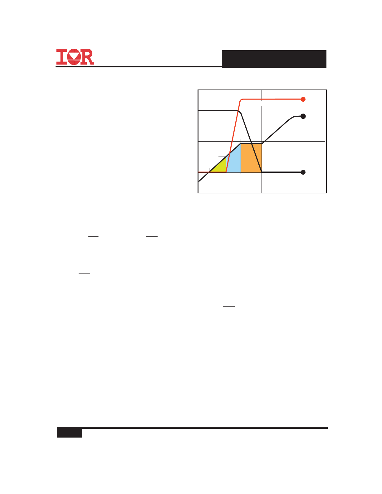
Fig 1.
Q
gs2
indicates the charge that must be supplied by
the gate driver between the time that the threshold
voltage has been reached (t1) and the time the drain
current rises to I
dmax
(t2) at which time the drain volt-
age begins to change. Minimizing Q
gs2
is a critical fac-
tor in reducing switching losses in Q1.
Q
oss
is the charge that must be supplied to the out-
put capacitance of the MOSFET during every switch-
ing cycle. Figure 2 shows how Q
oss
is formed by the
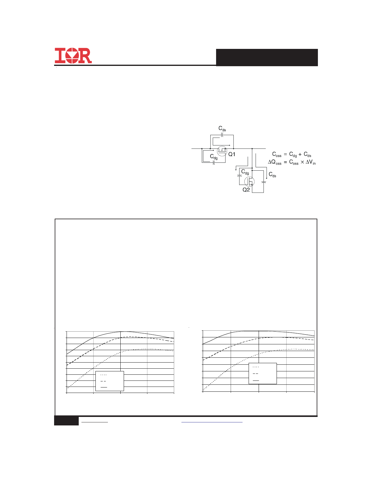
parallel combination of the voltage dependant (non-
linear) capacitance’s C
ds
and C
dg
when multiplied by
the power supply input buss voltage.
Figure 1: Typical MOSFET switching waveform
Synchronous FET
The power loss equation for Q2 is approximated
by;
P
loss
= P
conduction
+ P
drive
+ P
output
*
P
loss
= I
rms
2
× R
ds(on)
(
)
+ Q
g
× V
g
× f
(
)
+
Q
oss
2
× V
in
× f
⎛
⎝
⎜
⎞
⎠
+ Q
rr
× V
in
× f
(
)
*dissipated primarily in Q1.
Power MOSFET Selection for DC/DC
Converters
4
1
2
Drain Current
Gate Voltage
Drain Voltage
t3
t2
t1
V
GTH
Q
GS1
Q
GS2
Q
GD
t0
IRF7807VTRPbF-1
4
www.irf.com
©
2014 International Rectifier
Submit Datasheet Feedback
October 16, 2014
Typical Mobile PC Application
The performance of these new devices has been tested
in circuit and correlates well with performance predic-
tions generated by the system models. An advantage of
this new technology platform is that the MOSFETs it
produces are suitable for both control FET and synchro-
nous FET applications. This has been demonstrated with
the 3.3V and 5V converters. (Fig 3 and Fig 4). In these
applications the same MOSFET IRF7807V was used for
both the control FET (Q1) and the synchronous FET
(Q2). This provides a highly effective cost/performance
solution.
Figure 3
Figure 4
Figure 2: Q
oss
Characteristic
For the synchronous MOSFET Q2, R
ds(on)
is an im-
portant characteristic; however, once again the im-
portance of gate charge must not be overlooked since
it impacts three critical areas. Under light load the
MOSFET must still be turned on and off by the con-
trol IC so the gate drive losses become much more
significant. Secondly, the output charge Q
oss
and re-
verse recovery charge Q
rr
both generate losses that
are transfered to Q1 and increase the dissipation in
that device. Thirdly, gate charge will impact the
MOSFETs’ susceptibility to Cdv/dt turn on.
The drain of Q2 is connected to the switching node
of the converter and therefore sees transitions be-
tween ground and V
in
. As Q1 turns on and off there is
a rate of change of drain voltage dV/dt which is ca-
pacitively coupled to the gate of Q2 and can induce
a voltage spike on the gate that is sufficient to turn
the MOSFET on, resulting in shoot-through current .
The ratio of Q
gd
/Q
gs1
must be minimized to reduce the
potential for Cdv/dt turn on.
Spice model for IRF7807V can be downloaded in
machine readable format at www.irf.com.
3.3V Supply : Q1=Q2= IRF7807V
5.0V Supply : Q1=Q2= IRF7807V
83
84
85
86
87
88
89
90
91
92
93
1
2
3
4
5
Load current (A)
E
ffi
ci
en
cy (
%
)
Vin=24V
Vin=14V
Vin=10V
86
87
88
89
90
91
92
93
94
95
1
2
3
4
5
Load current (A)
Ef
fici
en
cy (%)
Vin=24V
Vin=14V
Vin=10V
5
www.irf.com
©
2014 International Rectifier
Submit Datasheet Feedback
October 16, 2014
IRF7807VTRPbF-1
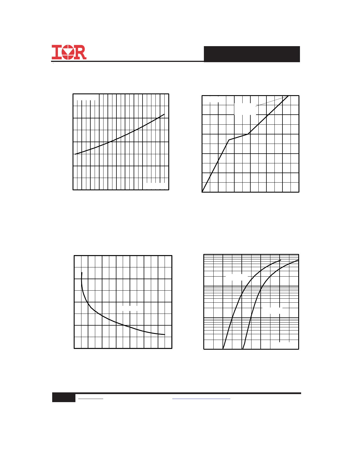
Fig 5. Normalized On-Resistance
Vs. Temperature
Fig 6. Typical Gate Charge Vs.
Gate-to-Source Voltage
Fig 7. On-Resistance Vs. Gate Voltage
Fig 8. Typical Source-Drain Diode
Forward Voltage
-60 -40 -20
0
20 40 60 80 100 120 140 160
0.0
0.5
1.0
1.5
2.0
T , Junction Temperature ( C)
R , Drain-to-Source On Resistance
(Normalized)
J
D
S
(on)
°
V
=
I =
GS
D
4.5V
7.0A
0
2
4
6
8
10
12
0
1
2
3
4
5
Q , Total Gate Charge (nC)
V , Gate-to-Source Voltage (V)
G
GS
I =
D
7.0A
V
= 16V
DS
0.1
1
10
100
0.2
0.4
0.6
0.8
1.0
1.2
V ,Source-to-Drain Voltage (V)
I , Reverse Drain Current (A)
SD
SD
V = 0 V
GS
T = 25 C
J
°
T = 150 C
J
°
2.0
4.0
6.0
8.0
10.0
12.0
14.0
16.0
VGS, Gate -to -Source Voltage (V)
0.010
0.015
0.020
0.025
0.030
R
D
S
(o
n)
,
D
ra
in
-t
o
-S
ou
rc
e
O
n
R
es
is
ta
nc
e
(Ω
)
ID = 7.0A
IRF7807VTRPbF-1
6
www.irf.com
©
2014 International Rectifier
Submit Datasheet Feedback
October 16, 2014
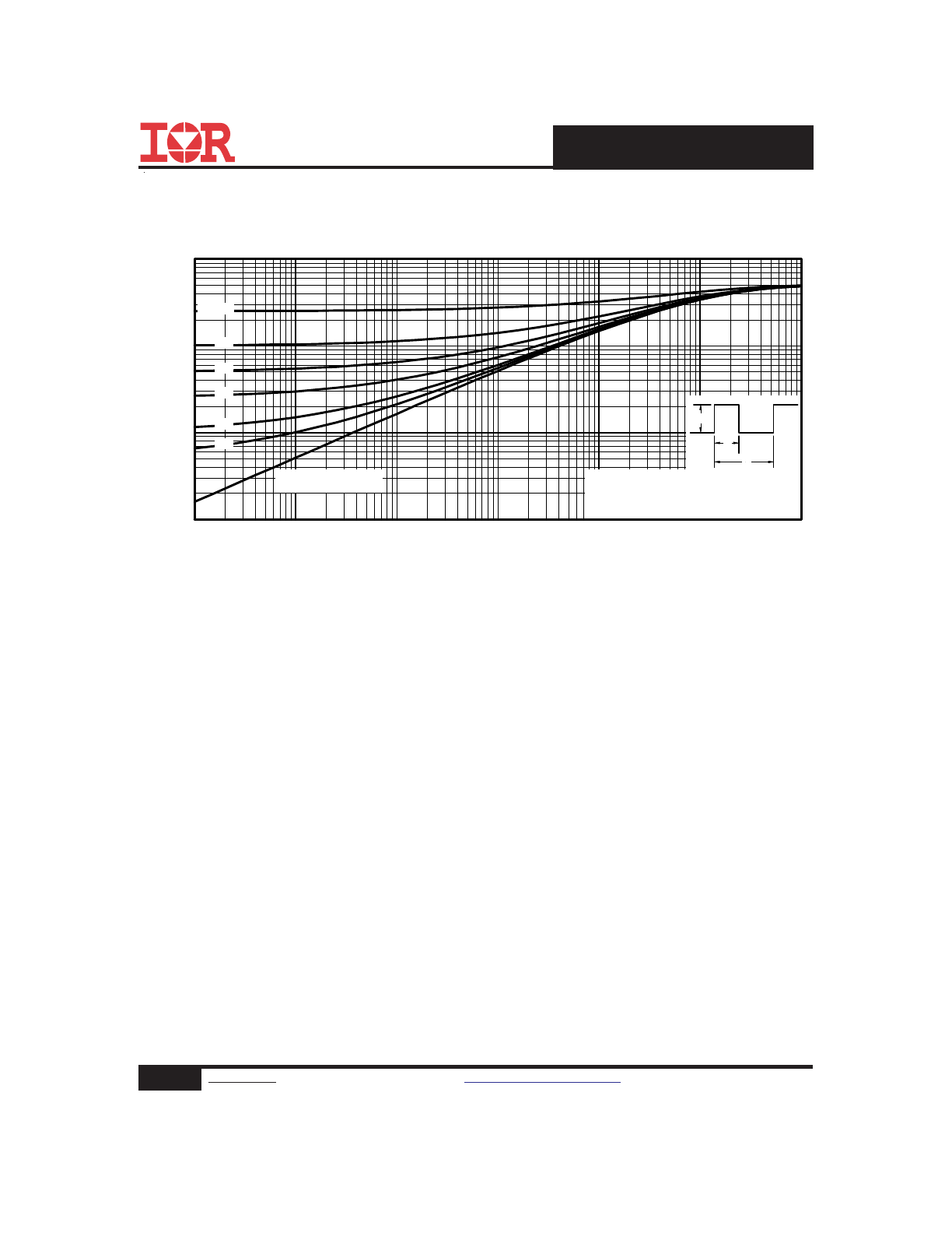
Figure 9. Maximum Effective Transient Thermal Impedance, Junction-to-Ambient
0.1
1
10
100
0.00001
0.0001
0.001
0.01
0.1
1
10
Notes:
1. Duty factor D = t / t
2. Peak T = P
x Z
+ T
1
2
J
DM
thJA
A
P
t
t
DM
1
2
t , Rectangular Pulse Duration (sec)
Ther
m
al
R
esponse
(Z
)
1
th
JA
0.01
0.02
0.05
0.10
0.20
D = 0.50
SINGLE PULSE
(THERMAL RESPONSE)
7
www.irf.com
©
2014 International Rectifier
Submit Datasheet Feedback
October 16, 2014
IRF7807VTRPbF-1
SO-8 Package Outline
Dimensions are shown in milimeters (inches)
e 1
D
E
y
b
A
A1
H
K
L
.189
.1497
0°
.013
.050 BASIC
.0532
.0040
.2284
.0099
.016
.1968
.1574
8°
.020
.0688
.0098
.2440
.0196
.050
4.80
3.80
0.33
1.35
0.10
5.80
0.25
0.40
0°
1.27 BASIC
5.00
4.00
0.51
1.75
0.25
6.20
0.50
1.27
MIN
MAX
MILLIMETERS
INCHES
MIN
MAX
DIM
8°
e
c
.0075
.0098
0.19
0.25
.025 BASIC
0.635 BAS IC
8
7
5
6
5
D
B
E
A
e
6X
H
0.25 [.010]
A
6
7
K x 45°
8X L
8X c
y
0.25 [.010]
C A B
e1
A
A1
8X b
C
0.10 [.004]
4
3
1
2
FOOTPRINT
8X 0.72 [.028]
6.46 [.255]
3X 1.27 [.050]
4. OUTLINE CONFORMS TO JEDEC OUTLINE MS-012AA.
NOTES:
1. DIMENSIONING & TOLERANCING PER ASME Y14.5M-1994.
2. CONTROLLING DIMENSION: MILLIMETER
3. DIMENSIONS ARE SHOWN IN MILLIMETERS [INCHES].
5 DIMENSION DOES NOT INCLUDE MOLD PROTRUSIONS.
6 DIMENSION DOES NOT INCLUDE MOLD PROTRUSIONS.
MOLD PROTRUSIONS NOT TO EXCEED 0.25 [.010].
7 DIMENSION IS THE LENGTH OF LEAD FOR SOLDERING TO
A SUBSTRATE.
MOLD PROTRUSIONS NOT TO EXCEED 0.15 [.006].
8X 1.78 [.070]
SO-8 Part Marking Information (Lead-Free)
DATE CODE (YWW)
XXXX
INTERNATIONAL
RECTIFIER
LOGO
F7101
Y = LAST DIGIT OF THE YEAR
PART NUMBER
LOT CODE
WW = WEEK
EXAMPLE: THIS IS AN IRF7101 (MOSFET)
P = DES IGNATES LEAD-FREE
PRODUCT (OPTIONAL)
A = AS SEMBLY S ITE CODE
Note: For the most current drawing please refer to IR website at:
http://www.irf.com/package/
IRF7807VTRPbF-1
8
www.irf.com
©
2014 International Rectifier
Submit Datasheet Feedback
October 16, 2014
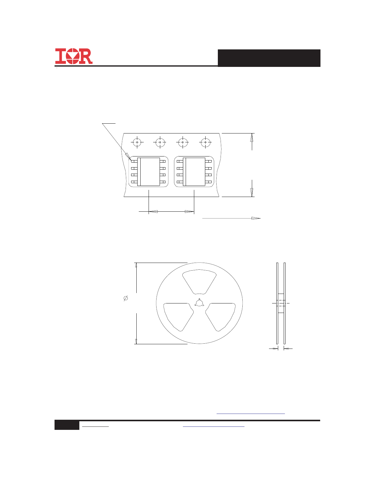
330.00
(12.992)
MAX.
14.40 ( .566 )
12.40 ( .488 )
NOTES :
1. CONTROLLING DIMENSION : MILLIMETER.
2. OUTLINE CONFORMS TO EIA-481 & EIA-541.
FEED DIRECTION
TERMINAL NUMBER 1
12.3 ( .484 )
11.7 ( .461 )
8.1 ( .318 )
7.9 ( .312 )
NOTES:
1. CONTROLLING DIMENSION : MILLIMETER.
2. ALL DIMENSIONS ARE SHOWN IN MILLIMETERS(INCHES).
3. OUTLINE CONFORMS TO EIA-481 & EIA-541.
SO-8 Tape and Reel
(Dimensions are shown in milimeters (inches))
Note: For the most current drawing please refer to IR website at:
http://www.irf.com/package/
9
www.irf.com
©
2014 International Rectifier
Submit Datasheet Feedback
October 16, 2014
IRF7807VTRPbF-1
† Qualification standards can be found at International Rectifier’s web site:
http://www.irf.com/product-info/reliability
††
Applicable version of JEDEC standard at the time of product release
IR WORLD HEADQUARTERS: 101 N. Sepulveda Blvd., El Segundo, California 90245, USA
To contact International Rectifier, please visit
http://www.irf.com/whoto-call/
MS L1
(per JEDEC J-S TD-020D
††
)
RoHS compliant
Yes
Qualification information
†
Qualification level
Industrial
(per JEDEC JES D47F
††
guidelines)
Moisture Sensitivity Level
SO-8
Date
Comments
• Corrected part number from" IRF7807VPbF-1" to "IRF7807VTRPbF-1" -all pages
• Removed the "IRF7807VPbF-1" bulk part number from ordering information on page1
Revision History
10/16/2014