
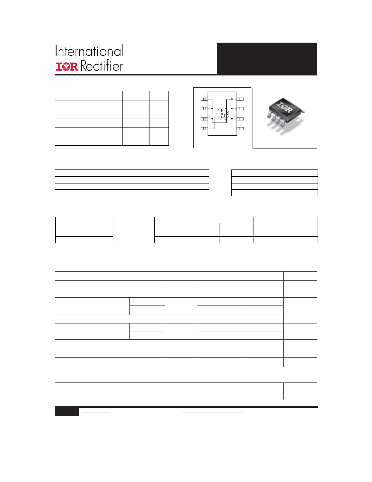
HEXFET
®
Chip-Set for DC-DC Converters
T op V iew
8
1
2
3
4
5
6
7
D
D
D
D
G
S
A
S
S
IRF7807TRPbF-1
IRF7807ATRPbF-1
SO-8
Features
Benefits
Industry-standard pinout SO-8 Package
⇒
Multi-Vendor Compatibility
Compatible with Existing Surface Mount Techniques
Easier Manufacturing
RoHS Compliant, Halogen-Free
Environmentally Friendlier
MSL1, Industrial qualification
Increased Reliability
Parameter
Symbol
IRF7807
IRF7807A
Units
Drain-Source Voltage
V
DS
30
V
Gate-Source Voltage
V
GS
±12
Continuous Drain or Source
25°C
I
D
8.3
8.3
A
Current (V
GS
≥ 4.5V)
70°C
6.6
6.6
Pulsed Drain Current
I
DM
66
66
Power Dissipation
25°C
P
D
2.5
W
70°C
1.6
Junction & Storage Temperature Range
T
J
,
T
STG
–55 to 150
°C
Continuous Source Current (Body Diode)
I
S
2.5
2.5
A
Pulsed source Current
I
SM
66
66
Absolute Maximum Ratings
Parameter
Max.
Units
Maximum Junction-to-Ambient
R
θJA
50
°C/W
Thermal Resistance
V
DS
30
V
R
DS(on) max
(@V
GS
= 4.5V)
25
Q
g (typical)
12
nC
I
D
(@T
A
= 25°C)
8.3
A
mΩ
1
www.irf.com
©
2014 International Rectifier
Submit Datasheet Feedback
October 16, 2014
Form
Quantity
IRF7807PbF-1
Tape and Reel
4000
IRF7807TRPbF-1
IRF7807APbF-1
Tape and Reel
4000
IRF7807ATRPbF-1
Package Type
Standard Pack
Orderable Part Number
Base Part Number
SO-8
IRF7807/ATRPbF-1
2
www.irf.com
©
2014 International Rectifier
Submit Datasheet Feedback
October 16, 2014
Parameter
Min Typ Max
Min Typ Max Units
Conditions
Diode Forward
V
SD
1.2
1.2
V
I
S
= 7A
, V
GS
= 0V
Voltage*
Reverse Recovery
Q
rr
80
80
nC di/dt = 700A/μs
Charge
V
DS
= 16V, V
GS
= 0V, I
S
= 7A
Reverse Recovery
Q
rr(s)
50
50
Charge (with Parallel
Schotkky)
Repetitive rating; pulse width limited by max. junction temperature.
Pulse width
≤ 300 μs; duty cycle ≤ 2%.
When mounted on 1 inch square copper board, t < 10 sec.
Typ = measured - Q
oss
*
Devices are 100% tested to these parameters.
Parameter
Min Typ Max
Min Typ Max Units
Conditions
Drain-to-Source
V
(BR)DSS
30
–
–
30
–
–
V
V
GS
= 0V, I
D
= 250μA
Breakdown Voltage*
Static Drain-Source
R
DS
(on)
17
25
17
25
m
Ω
V
GS
= 4.5V, I
D
= 7A
on Resistance*
Gate Threshold Voltage* V
GS
(th)
1.0
1.0
V
V
DS
= V
GS
, I
D
= 250μA
Drain-Source Leakage
I
DSS
30
30
μA
V
DS
= 24V, V
GS
= 0
150
150
V
DS
= 24V, V
GS
= 0,
Tj = 100°C
Gate-Source Leakage
I
GSS
±100
±100 nA
V
GS
= ±12V
Current*
Total Gate Charge*
Q
g
12
17
12
17
V
GS
= 5V, I
D
= 7A
Pre-Vth
Q
gs1
2.1
2.1
V
DS
= 16V, I
D
= 7A
Gate-Source Charge
Post-Vth
Q
gs2
0.76
0.76
nC
Gate-Source Charge
Gate to Drain Charge
Q
gd
2.9
2.9
Switch Charge*
Q
SW
3.66
5.2
3.66
(Q
gs2
+ Q
gd
)
Output Charge*
Q
oss
14
16.8
14
16.8
V
DS
= 16V, V
GS
= 0
Gate Resistance
R
g
1.2
1.2
Ω
Turn-on Delay Time
t
d
(on)
12
12
V
DD
= 16V
Rise Time
t
r
17
17
ns
I
D
= 7A
Turn-off Delay Time
t
d
(off)
25
25
R
g
= 2
Ω
Fall Time
t
f
6
6
V
GS
= 4.5V
Resistive Load
Electrical Characteristics
Source-Drain Rating & Characteristics
Notes:
IRF7807
IRF7807A
Current*
di/dt = 700A/μs
(with 10BQ040)
V
DS
= 16V, V
GS
= 0V, I
S
= 7A
3
www.irf.com
©
2014 International Rectifier
Submit Datasheet Feedback
October 16, 2014
IRF7807/ATRPbF-1
Control FET
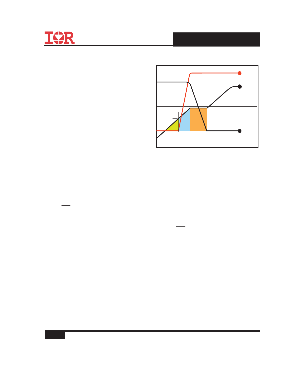
Special attention has been given to the power losses
in the switching elements of the circuit - Q1 and Q2.
Power losses in the high side switch Q1, also called the
Control FET, are impacted by the R
ds(on)
of the MOSFET,
but these conduction losses are only about one half of
the total losses.
Power losses in the control switch Q1 are given by;
P
loss
= P
conduction
+ P
switching
+ P
drive
+ P
output
This can be expanded and approximated by;
P
loss
= I
rms
2
× R
ds(on )
(
)
+ I ×
Q
gd
i
g
× V
in
× f
⎛
⎝
⎜
⎞
⎠
⎟ + I ×
Q
gs2
i
g
× V
in
× f
⎛
⎝
⎜
⎞
⎠
⎟
+ Q
g
× V
g
× f
(
)
+
Q
oss
2
×V
in
× f
⎛
⎝
⎞
⎠
This simplified loss equation includes the terms Q
gs2
and Q
oss
which are new to Power MOSFET data sheets.
Q
gs2
is a sub element of traditional gate-source charge
that is included in all MOSFET data sheets. The impor-
tance of splitting this gate-source charge into two sub
elements, Q
gs1
and Q
gs2
, can be seen from Fig 1.
Q
gs2
indicates the charge that must be supplied by
the gate driver between the time that the threshold volt-
age has been reached (t1) and the time the drain cur-
rent rises to I
dmax
(t2) at which time the drain voltage
begins to change. Minimizing Q
gs2
is a critical factor in
reducing switching losses in Q1.
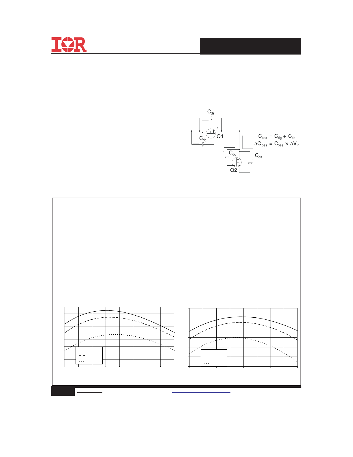
Q
oss
is the charge that must be supplied to the output
capacitance of the MOSFET during every switching
cycle. Figure 2 shows how Q
oss
is formed by the paral-
lel combination of the voltage dependant (non-linear)
capacitance’s C
ds
and C
dg
when multiplied by the power
supply input buss voltage.
Figure 1: Typical MOSFET switching waveform
Synchronous FET
The power loss equation for Q2 is approximated
by;
P
loss
= P
conduction
+ P
drive
+ P
output
*
P
loss
= I
rms
2
× R
ds(on)
(
)
+ Q
g
× V
g
× f
(
)
+
Q
oss
2
×V
in
× f
⎛
⎝
⎜
⎞
⎠
+ Q
rr
× V
in
× f
(
)
*dissipated primarily in Q1.
Power MOSFET Selection for DC/DC
Converters
4
1
2
Drain Current
Gate Voltage
Drain Voltage
t3
t2
t1
V
GTH
Q
GS1
Q
GS2
Q
GD
t0
IRF7807/ATRPbF-1
4
www.irf.com
©
2014 International Rectifier
Submit Datasheet Feedback
October 16, 2014
5V Supply : Q1=Q2=IRF7807
89
90
91
92
93
94
95
1
1.5
2
2.5
3
3.5
4
4.5
5
Load Current (A)
Ef
fici
en
cy (%
)
Vin = 10V
Vin = 14V
Vin=24V
Typical Mobile PC Application
The performance of these new devices has been tested
in circuit and correlates well with performance predic-
tions generated by the system models. An advantage
of this new technology platform is that the MOSFETs
it produces are suitable for both control FET and syn-
chronous FET applications. This has been demon-
strated with the 3.3V and 5V converters. (Fig 3 and
Fig 4). In these applications the same MOSFET IRF7807
was used for both the control FET (Q1) and the syn-
chronous FET (Q2). This provides a highly effective
cost/performance solution.
3.3V Supply : Q1=Q2=IRF7807
84
85
86
87
88
89
90
91
92
93
1
1.5
2
2.5
3
3.5
4
4.5
5
Load Current (A)
Ef
fici
en
cy (%
)
Vin = 10V
Vin = 14V
Vin = 24V
Figure 3
Figure 4
Figure 2: Q
oss
Characteristic
For the synchronous MOSFET Q2, R
ds(on)
is an im-
portant characteristic; however, once again the impor-
tance of gate charge must not be overlooked since it
impacts three critical areas. Under light load the
MOSFET must still be turned on and off by the con-
trol IC so the gate drive losses become much more
significant. Secondly, the output charge Q
oss
and re-
verse recovery charge Q
rr
both generate losses that
are transfered to Q1 and increase the dissipation in
that device. Thirdly, gate charge will impact the
MOSFETs’ susceptibility to Cdv/dt turn on.
The drain of Q2 is connected to the switching node
of the converter and therefore sees transitions be-
tween ground and V
in
. As Q1 turns on and off there is
a rate of change of drain voltage dV/dt which is ca-
pacitively coupled to the gate of Q2 and can induce
a voltage spike on the gate that is sufficient to turn
the MOSFET on, resulting in shoot-through current .
The ratio of Q
gd
/Q
gs1
must be minimized to reduce the
potential for Cdv/dt turn on.
Spice model for IRF7807 can be downloaded in ma-
chine readable format at www.irf.com.
5
www.irf.com
©
2014 International Rectifier
Submit Datasheet Feedback
October 16, 2014
IRF7807/ATRPbF-1
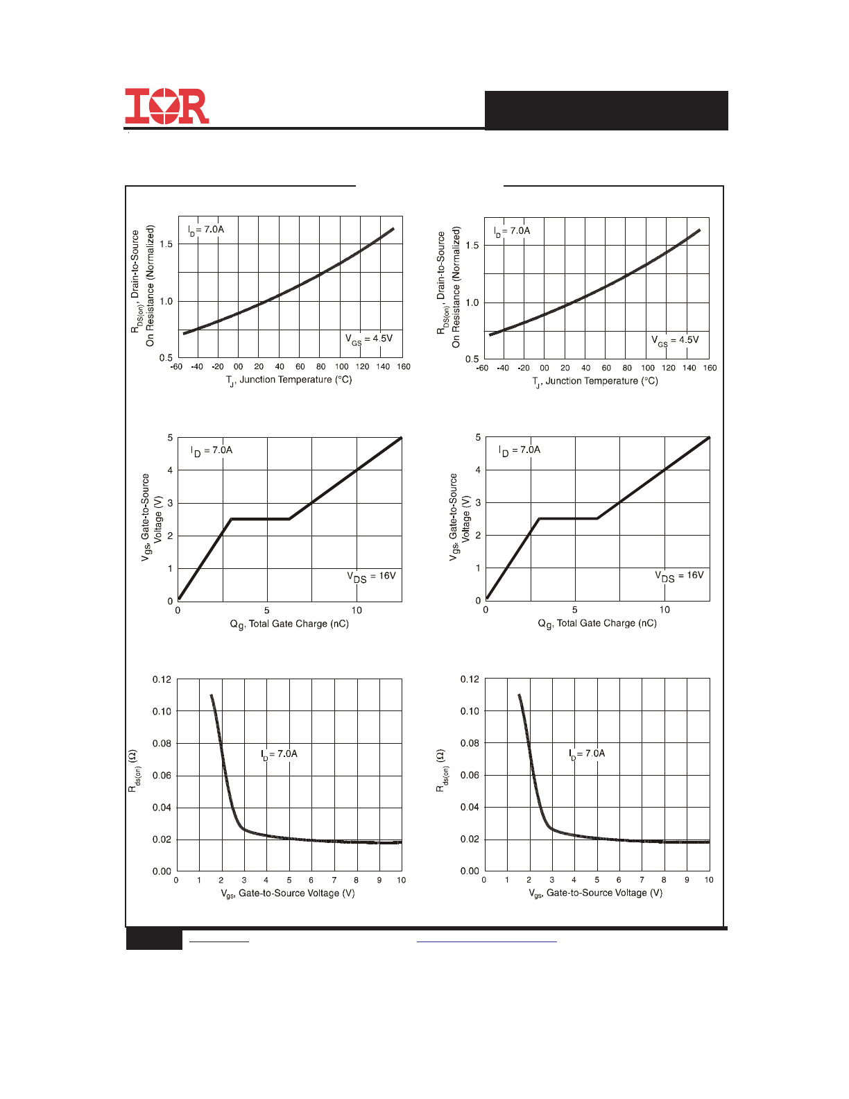
Figure 9. Typical Rds(on) vs. Gate-to-Source Voltage
Figure 7. Typical Gate Charge vs. Gate-to-Source Voltage
Figure 5. Normalized On-Resistance vs. Temperature
Figure 10. Typical Rds(on) vs. Gate-to-Source Voltage
Figure 8. Typical Gate Charge vs. Gate-to-Source Voltage
Figure 6. Normalized On-Resistance vs. Temperature
IRF7807
IRF7807A
Typical Characteristics
IRF7807/ATRPbF-1
6
www.irf.com
©
2014 International Rectifier
Submit Datasheet Feedback
October 16, 2014
0.1
1
10
0.4
0.5
0.6
0.7
0.8
0.9
V ,Source-to-Drain Voltage (V)
I ,
R
ever
se D
rai
n C
ur
rent
(
A
)
SD
SD
V = 0 V
GS
T = 25 C
J
°
T = 150 C
J
°
IRF7807
IRF7807A
0.1
1
10
100
0.001
0.01
0.1
1
10
100
1000
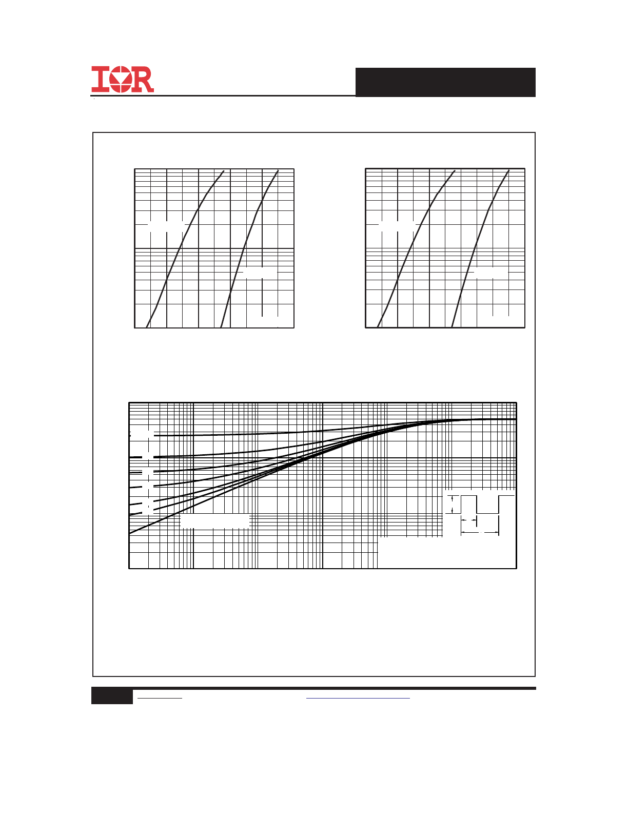
Notes:
1. Duty factor D = t / t
2. Peak T = P
x Z
+ T
1
2
J
DM
thJA
A
P
t
t
DM
1
2
t , Rectangular Pulse Duration (sec)
Thermal Response
(Z )
1
thJA
0.01
0.02
0.05
0.10
0.20
D = 0.50
SINGLE PULSE
(THERMAL RESPONSE)
Figure 11. Typical Source-Drain Diode Forward Voltage
Figure 12. Typical Source-Drain Diode Forward Voltage
Figure 13. Maximum Effective Transient Thermal Impedance, Junction-to-Ambient
0.1
1
10
0.4
0.5
0.6
0.7
0.8
0.9
V ,Source-to-Drain Voltage (V)
I ,
R
ever
se D
rai
n C
ur
rent
(
A
)
SD
SD
V = 0 V
GS
T = 25 C
J
°
T = 150 C
J
°
7
www.irf.com
©
2014 International Rectifier
Submit Datasheet Feedback
October 16, 2014
IRF7807/ATRPbF-1
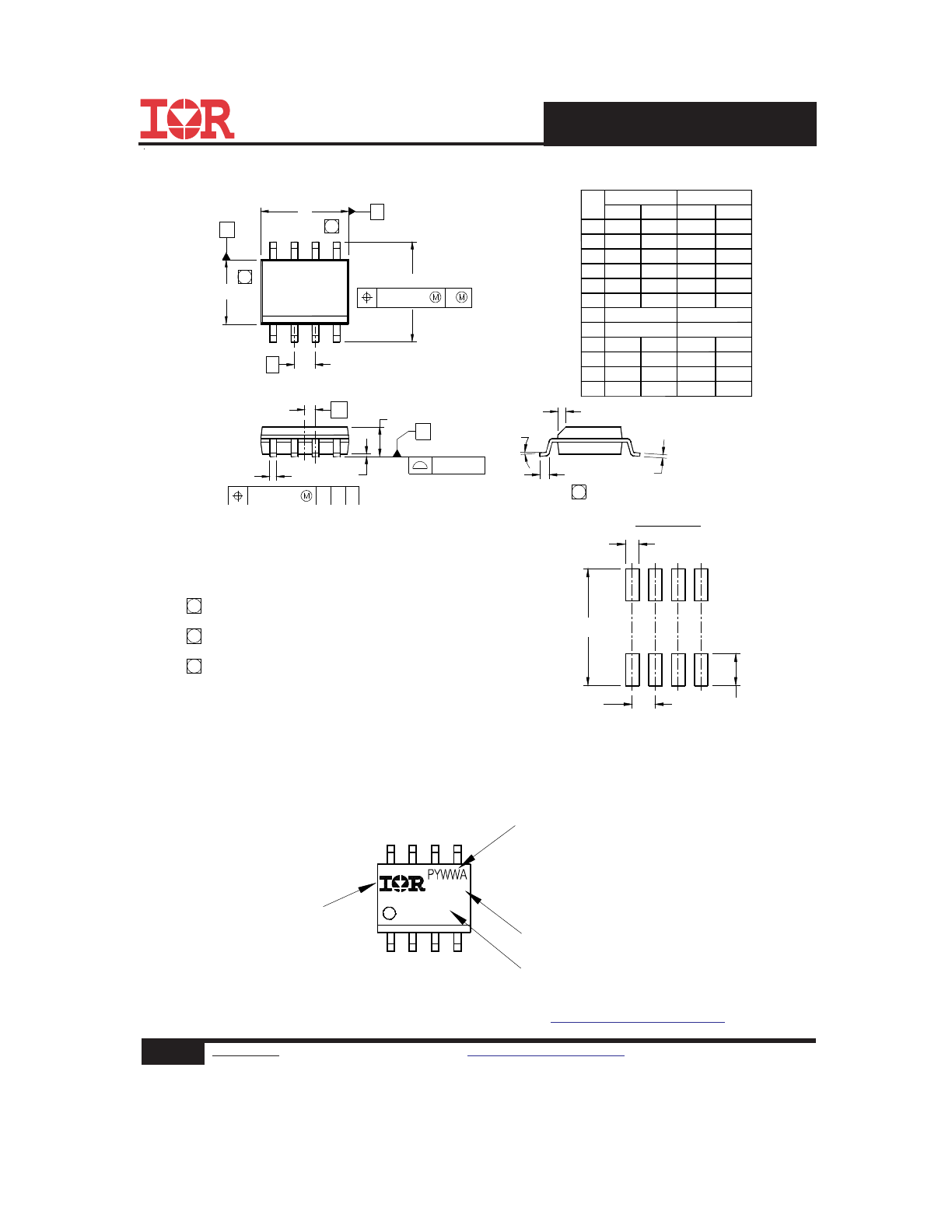
SO-8 Package Outline
Dimensions are shown in millimeters (inches)
SO-8 Part Marking
e 1
D
E
y
b
A
A1
H
K
L
.189
.1497
0°
.013
.050 BASIC
.0532
.0040
.2284
.0099
.016
.1968
.1574
8°
.020
.0688
.0098
.2440
.0196
.050
4.80
3.80
0.33
1.35
0.10
5.80
0.25
0.40
0°
1.27 BASIC
5.00
4.00
0.51
1.75
0.25
6.20
0.50
1.27
MIN
MAX
MILLIMETERS
INCHES
MIN
MAX
DIM
8°
e
c
.0075
.0098
0.19
0.25
.025 BASIC
0.635 BASIC
8
7
5
6
5
D
B
E
A
e
6X
H
0.25 [.010]
A
6
7
K x 45°
8X L
8X c
y
0.25 [.010]
C A B
e1
A
A1
8X b
C
0.10 [.004]
4
3
1
2
FOOTPRINT
8X 0.72 [.028]
6.46 [.255]
3X 1.27 [.050]
4. OUTLINE CONFORMS TO JEDEC OUTLINE MS-012AA.
NOT ES:
1. DIMENSIONING & TOLERANCING PER ASME Y14.5M-1994.
2. CONT ROLLING DIMENSION: MILLIMET ER
3. DIMENSIONS ARE SHOWN IN MILLIMETERS [INCHES].
5 DIMENSION DOES NOT INCLUDE MOLD PROT RUSIONS.
6 DIMENSION DOES NOT INCLUDE MOLD PROT RUSIONS.
MOLD PROTRUSIONS NOT TO EXCEED 0.25 [.010].
7 DIMENSION IS T HE LENGT H OF LEAD FOR SOLDERING TO
A SUBST RAT E.
MOLD PROTRUSIONS NOT TO EXCEED 0.15 [.006].
8X 1.78 [.070]
DATE CODE (YWW)
XXXX
INTERNATIONAL
RECTIFIER
LOGO
F7101
Y = LAS T DIGIT OF THE YEAR
PART NUMBER
LOT CODE
WW = WEEK
EXAMPLE: THIS IS AN IRF7101 (MOSFET)
P = DESIGNATES LEAD-FREE
PRODUCT (OPTIONAL)
A = ASSEMBLY SITE CODE
Note: For the most current drawing please refer to IR website at:
http://www.irf.com/package/
IRF7807/ATRPbF-1
8
www.irf.com
©
2014 International Rectifier
Submit Datasheet Feedback
October 16, 2014
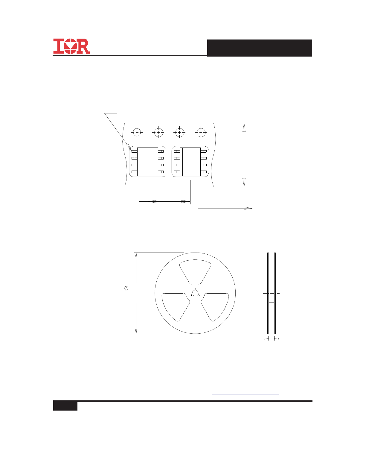
330.00
(12.992)
MAX.
14.40 ( .566 )
12.40 ( .488 )
NOTES :
1. CONTROLLING DIMENSION : MILLIMETER.
2. OUTLINE CONFORMS TO EIA-481 & EIA-541.
FEED DIRECTION
TERMINAL NUMBER 1
12.3 ( .484 )
11.7 ( .461 )
8.1 ( .318 )
7.9 ( .312 )
NOTES:
1. CONTROLLING DIMENSION : MILLIMETER.
2. ALL DIMENSIONS ARE SHOWN IN MILLIMETERS(INCHES).
3. OUTLINE CONFORMS TO EIA-481 & EIA-541.
SO-8 Tape and Reel
(Dimensions are shown in millimeters (inches))
Note: For the most current drawing please refer to IR website at:
http://www.irf.com/package/
9
www.irf.com
©
2014 International Rectifier
Submit Datasheet Feedback
October 16, 2014
IRF7807/ATRPbF-1
† Qualification standards can be found at International Rectifier’s web site:
http://www.irf.com/product-info/reliability
††
Applicable version of JEDEC standard at the time of product release
IR WORLD HEADQUARTERS: 101 N. Sepulveda Blvd., El Segundo, California 90245, USA
To contact International Rectifier, please visit
http://www.irf.com/whoto-call/
MS L1
(per JEDEC J-S TD-020D
††
)
RoHS compliant
Yes
Qualification information
†
Qualification level
Industrial
(per JEDEC JES D47F
††
guidelines)
Moisture Sensitivity Level
SO-8
Date
Comments
• Corrected part number from" IRF7807/APbF-1" to "IRF7807/ATRPbF-1" -all pages
• Removed the "IRF7807/APbF-1" bulk part number from ordering information on page1
Revision History
10/16/2014