
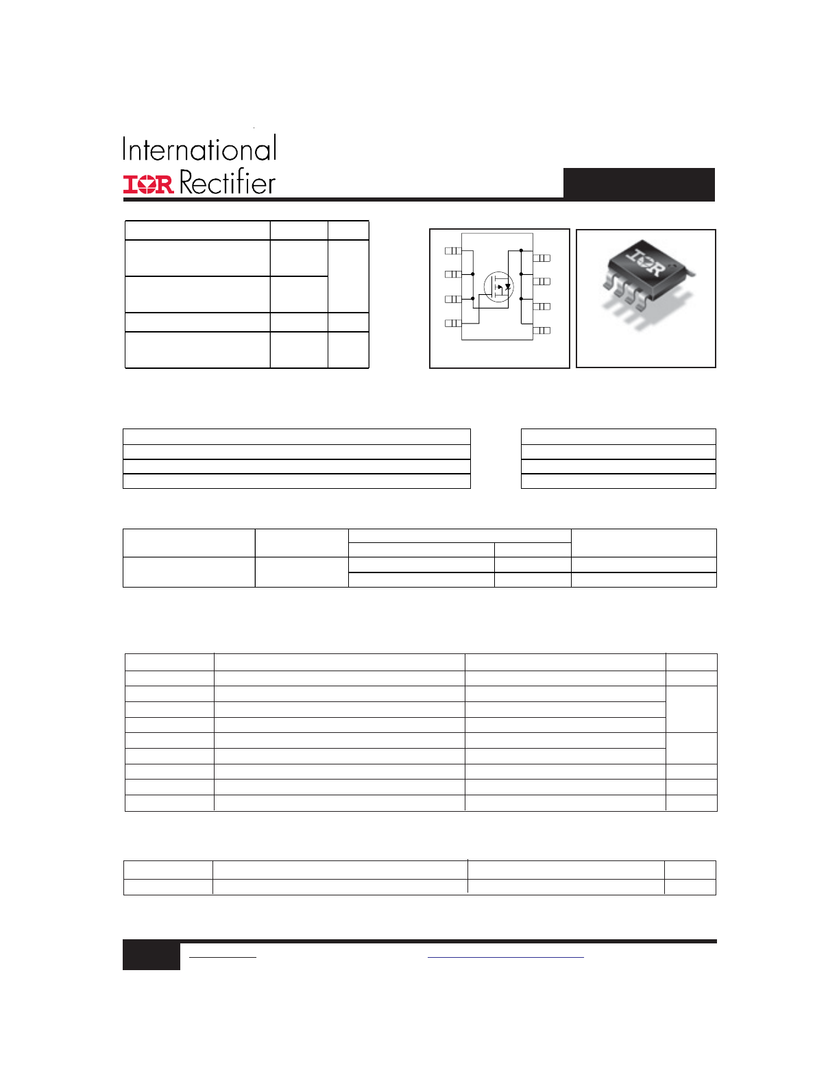
HEXFET
®
Power MOSFET
Top View
8
1
2
3
4
5
6
7
D
D
D
G
S
A
D
S
S
SO-8
IRF7425PbF
Parameter
Max.
Units
R
θJA
Maximum Junction-to-Ambient
50
°C/W
Thermal Resistance
Parameter
Max.
Units
V
DS
Drain- Source Voltage
-20
V
I
D
@ T
A
= 25°C
Continuous Drain Current, V
GS
@ -4.5V
-15
I
D
@ T
A
= 70°C
Continuous Drain Current, V
GS
@ -4.5V
-12
A
I
DM
Pulsed Drain Current
-60
P
D
@T
A
= 25°C
Power Dissipation
2.5
P
D
@T
A
= 70°C
Power Dissipation
1.6
Linear Derating Factor
20
mW/°C
V
GS
Gate-to-Source Voltage
± 12
V
T
J,
T
STG
Junction and Storage Temperature Range
-55 to + 150
°C
Absolute Maximum Ratings
W
V
DS
-20
V
R
DS(on) max
(@V
GS
= -4.5V)
8.2
R
DS(on) max
(@V
GS
= -2.5V)
13
Q
g (typical)
87
nC
I
D
(@T
A
= 25°C)
-15
A
mΩ
Features
Benefits
Industry-standard pinout SO-8 Package
⇒
Multi-Vendor Compatibility
Compatible with Existing Surface Mount Techniques
Easier Manufacturing
RoHS Compliant, Halogen-Free
Environmentally Friendlier
MSL1,Consumer qualification
Increased Reliability
Form
Quantity
Tube/Bulk
95
IRF7425PbF
Tape and Reel
4000
IRF7425TRPbF
Package Type
Standard Pack
Orderable Part Number
IRF7425PbF
SO-8
Base Part Number
1
www.irf.com
©
2013 International Rectifier
Submit Datasheet Feedback
October 29, 2013
IRF7425PbF
2
www.irf.com
©
2013 International Rectifier
Submit Datasheet Feedback
October 29, 201
3
Parameter
Min. Typ. Max. Units
Conditions
I
S
Continuous Source Current
MOSFET symbol
(Body Diode)
showing the
I
SM
Pulsed Source Current
integral reverse
(Body Diode)
p-n junction diode.
V
SD
Diode Forward Voltage
–––
–––
-1.2
V
T
J
= 25°C, I
S
= -2.5A, V
GS
= 0V
t
rr
Reverse Recovery Time
–––
120 180
ns
T
J
= 25°C, I
F
= -2.5A
Q
rr
Reverse Recovery Charge
–––
160 240
nC
di/dt = -100A/μs
Source-Drain Ratings and Characteristics
A
-60
–––
–––
–––
-2.5
–––
S
D
G
Repetitive rating; pulse width limited by
max. junction temperature.
Notes:
Pulse width ≤ 400μs; duty cycle ≤ 2%.
Parameter
Min. Typ. Max. Units
Conditions
V
(BR)DSS
Drain-to-Source Breakdown Voltage
-20
–––
–––
V
V
GS
= 0V, I
D
= -250μA
ΔV
(BR)DSS
/
ΔT
J
Breakdown Voltage Temp. Coefficient
––– 0.010 –––
V/°C Reference to 25°C, I
D
= -1mA
––– –––
8.2
V
GS
= -4.5V, I
D
= -15A
––– –––
13
V
GS
= -2.5V, I
D
= -13A
V
GS(th)
Gate Threshold Voltage
-0.45 ––– -1.2
V
V
DS
= V
GS
, I
D
= -250μA
g
fs
Forward Transconductance
44
–––
–––
S
V
DS
= -10V, I
D
= -15A
––– ––– -1.0
V
DS
= -16V, V
GS
= 0V
––– –––
-25
V
DS
= -16V, V
GS
= 0V, T
J
= 70°C
Gate-to-Source Forward Leakage
––– ––– -100
V
GS
= -12V
Gate-to-Source Reverse Leakage
––– –––
100
V
GS
= 12V
Q
g
Total Gate Charge
–––
87
130
I
D
= -15A
Q
gs
Gate-to-Source Charge
–––
18
27
nC
V
DS
= -10V
Q
gd
Gate-to-Drain ("Miller") Charge
–––
21
32
V
GS
= -4.5V
t
d(on)
Turn-On Delay Time
–––
13
–––
V
DD
= -10V
t
r
Rise Time
–––
20
–––
I
D
= -1.0A
t
d(off)
Turn-Off Delay Time
––– 230
–––
R
G
= 6.0
Ω
t
f
Fall Time
––– 160
–––
V
GS
= -4.5V
C
iss
Input Capacitance
––– 7980 –––
V
GS
= 0V
C
oss
Output Capacitance
––– 1480 –––
pF
V
DS
= -15V
C
rss
Reverse Transfer Capacitance
––– 980
–––
ƒ = 1.0kHz
Electrical Characteristics @ T
J
= 25°C (unless otherwise specified)
I
GSS
µA
m
Ω
R
DS(on)
Static Drain-to-Source On-Resistance
I
DSS
Drain-to-Source Leakage Current
nA
ns
Surface mounted on 1 in square Cu board, t ≤ 10sec.
IRF7425PbF
3
www.irf.com
©
2013 International Rectifier
Submit Datasheet Feedback
October 29, 201
3
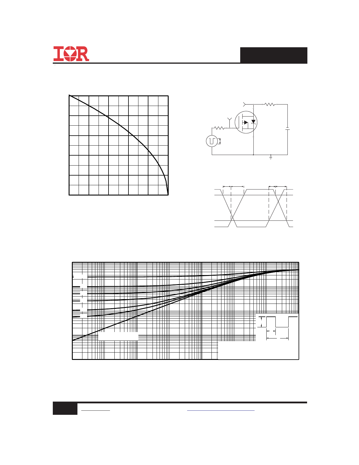
Fig 4. Normalized On-Resistance
Vs. Temperature
Fig 2. Typical Output Characteristics
Fig 1. Typical Output Characteristics
Fig 3. Typical Transfer Characteristics
0.01
0.1
1
10
100
1000
0.1
1
10
100
20μs PULSE WIDTH
T = 25 C
J
°
TOP
BOTTOM
VGS
-7.0V
-5.0V
-4.5V
-2.5V
-1.8V
-1.5V
-1.2V
-1.0V
-V , Drain-to-Source Voltage (V)
-I , Drain-to-Source Current (A)
DS
D
-1.0V
0.1
1
10
100
1000
0.1
1
10
100
20μs PULSE WIDTH
T = 150 C
J
°
TOP
BOTTOM
VGS
-7.0V
-5.0V
-4.5V
-2.5V
-1.8V
-1.5V
-1.2V
-1.0V
-V , Drain-to-Source Voltage (V)
-I , Drain-to-Source Current (A)
DS
D
-1.0V
0.1
1
10
100
1.0
1.2
1.4
1.6
1.8
2.0
2.2
V = -15V
20μs PULSE WIDTH
DS
-V , Gate-to-Source Voltage (V)
-I , Drain-to-Source Current (A)
GS
D
T = 25 C
J
°
T = 150 C
J
°
-60 -40 -20
0
20 40 60 80 100 120 140 160
0.0
0.5
1.0
1.5
2.0
T , Junction Temperature ( C)
R
, D
rain-to-S
ource O
n R
esistance
(Normalized)
J
D
S
(on)
°
V
=
I =
GS
D
-4.5V
-15A
IRF7425PbF
4
www.irf.com
©
2013 International Rectifier
Submit Datasheet Feedback
October 29, 201
3
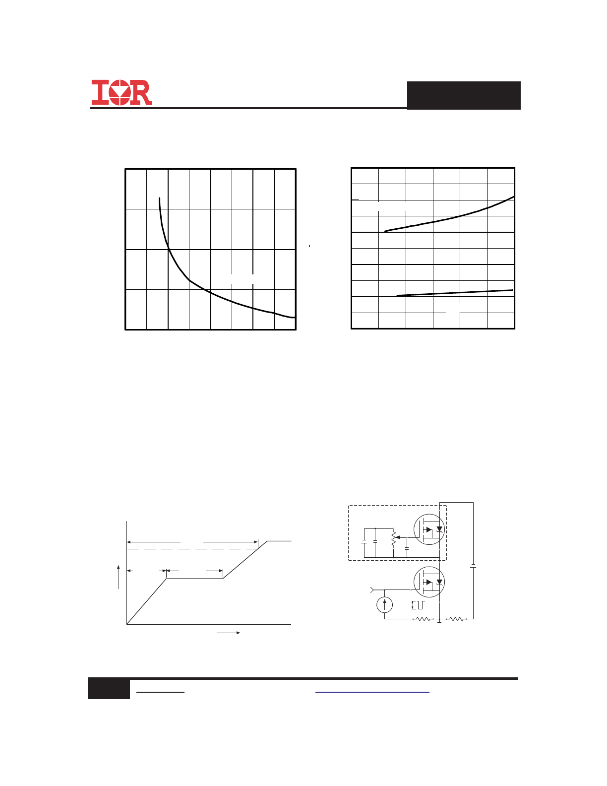
Fig 8. Maximum Safe Operating Area
Fig 6. Typical Gate Charge Vs.
Gate-to-Source Voltage
Fig 5. Typical Capacitance Vs.
Drain-to-Source Voltage
Fig 7. Typical Source-Drain Diode
Forward Voltage
0
40
80
120
160
0
2
4
6
8
Q , Total Gate Charge (nC)
-V , Gate-to-Source Voltage (V)
G
GS
I =
D
-15A
V
=-10V
DS
V
=-16V
DS
0.1
1
10
100
0.2
0.4
0.6
0.8
1.0
-V ,Source-to-Drain Voltage (V)
-I , Reverse Drain Current (A)
SD
SD
V = 0 V
GS
T = 25 C
J
°
T = 150 C
J
°
1
10
100
1000
0.1
1
10
100
OPERATION IN THIS AREA LIMITED
BY R
DS(on)
Single Pulse
T
T
= 150 C
= 25 C
°
°
J
A
-V , Drain-to-Source Voltage (V)
-I , Drain Current (A)I , Drain Current (A)
DS
D
100us
1ms
10ms
1
10
100
0
2000
4000
6000
8000
10000
12000
-V , Drain-to-Source Voltage (V)
C, Capacitance (pF)
DS
V
C
C
C
=
=
=
=
0V,
C
C
C
f = 1MHz
+ C
+ C
C SHORTED
GS
iss
gs
gd ,
ds
rss
gd
oss
ds
gd
C
iss
C
oss
C
rss
IRF7425PbF
5
www.irf.com
©
2013 International Rectifier
Submit Datasheet Feedback
October 29, 201
3
Fig 11. Maximum Effective Transient Thermal Impedance, Junction-to-Ambient
Fig 9. Maximum Drain Current Vs.
Case Temperature
25
50
75
100
125
150
0
3
6
9
12
15
T , Case Temperature ( C)
-I , Drain Current (A)
°
C
D
V
DS
V
GS
Pulse Width ≤ 1 µs
Duty Factor ≤ 0.1 %
R
D
V
GS
V
DD
R
G
D.U.T.
+
-
V
DS
90%
10%
V
GS
t
d(on)
t
r
t
d(off)
t
f
Fig 10a. Switching Time Test Circuit
Fig 10b. Switching Time Waveforms
0.01
0.1
1
10
100
0.00001
0.0001
0.001
0.01
0.1
1
10
100
Notes:
1. Duty factor D = t / t
2. Peak T = P
x Z
+ T
1
2
J
DM
thJA
A
P
t
t
DM
1
2
t , Rectangular Pulse Duration (sec)
Ther
m
al
Response
(Z
)
1
th
JA
0.01
0.02
0.05
0.10
0.20
D = 0.50
SINGLE PULSE
(THERMAL RESPONSE)
IRF7425PbF
6
www.irf.com
©
2013 International Rectifier
Submit Datasheet Feedback
October 29, 201
3
Fig 13. Typical On-Resistance Vs.
Drain Current
Fig 12. Typical On-Resistance Vs.
Gate Voltage
Fig 14b. Gate Charge Test Circuit
Fig 14a. Basic Gate Charge Waveform
Q
G
Q
GS
Q
GD
V
G
Charge
D.U.T.
V
DS
I
D
I
G
-3mA
V
GS
.3
μF
50K
Ω
.2
μF
12V
Current Regulator
Same Type as D.U.T.
Current Sampling Resistors
+
-
1.0
2.0
3.0
4.0
5.0
-VGS, Gate -to -Source Voltage (V)
0.005
0.010
0.015
R
D
S
(o
n)
,
D
ra
in
-t
o
-S
ou
rc
e
O
n
R
es
is
ta
nc
e
(Ω
)
ID = -15A
0
10
20
30
40
50
60
-ID , Drain Current (A)
0.005
0.006
0.007
0.008
0.009
0.010
R
D
S
(
on
)
, D
ra
in
-t
o-
S
ou
rc
e
O
n
R
es
is
ta
nc
e
(Ω
)
VGS = -2.5V
VGS = -4.5V
IRF7425PbF
7
www.irf.com
©
2013 International Rectifier
Submit Datasheet Feedback
October 29, 201
3
Fig 15. Typical Vgs(th) Variance Vs.
Juction Temperature
Fig 16
. Typical Power Vs. Time
-75
-50
-25
0
25
50
75
100 125 150
TJ , Temperature ( °C )
1.5
2.0
2.5
3.0
-V
G
S
(t
h)
,
V
ar
ia
ce
(
V
)
ID = -250μA
0.001
0.010
0.100
1.000
10.000
100.000
Time (sec)
0
20
40
60
80
100
120
P
ow
er
(
W
)
IRF7425PbF
8
www.irf.com
©
2013 International Rectifier
Submit Datasheet Feedback
October 29, 201
3
SO-8 Package Outline
Dimensions are shown in millimeters (inches)
SO-8 Part Marking
e 1
D
E
y
b
A
A1
H
K
L
.189
.1497
0°
.013
.050 BASIC
.0532
.0040
.2284
.0099
.016
.1968
.1574
8°
.020
.0688
.0098
.2440
.0196
.050
4.80
3.80
0.33
1.35
0.10
5.80
0.25
0.40
0°
1.27 BASIC
5.00
4.00
0.51
1.75
0.25
6.20
0.50
1.27
MIN
MAX
MILLIMETERS
INCHES
MIN
MAX
DIM
8°
e
c
.0075
.0098
0.19
0.25
.025 BASIC
0.635 BASIC
8
7
5
6
5
D
B
E
A
e
6X
H
0.25 [.010]
A
6
7
K x 45°
8X L
8X c
y
0.25 [.010]
C A B
e1
A
A1
8X b
C
0.10 [.004]
4
3
1
2
FOOTPRINT
8X 0.72 [.028]
6.46 [.255]
3X 1.27 [.050]
4. OUTLINE CONFORMS TO JEDEC OUTLINE MS-012AA.
NOT ES:
1. DIMENSIONING & TOLERANCING PER ASME Y14.5M-1994.
2. CONT ROLLING DIMENSION: MILLIMET ER
3. DIMENSIONS ARE SHOWN IN MILLIMETERS [INCHES].
5 DIMENSION DOES NOT INCLUDE MOLD PROT RUSIONS.
6 DIMENSION DOES NOT INCLUDE MOLD PROT RUSIONS.
MOLD PROTRUSIONS NOT TO EXCEED 0.25 [.010].
7 DIMENSION IS T HE LENGT H OF LEAD FOR SOLDERING TO
A SUBST RAT E.
MOLD PROTRUSIONS NOT TO EXCEED 0.15 [.006].
8X 1.78 [.070]
DATE CODE (YWW)
XXXX
INTERNATIONAL
RECTIFIER
LOGO
F7101
Y = LAS T DIGIT OF THE YEAR
PART NUMBER
LOT CODE
WW = WEEK
EXAMPLE: THIS IS AN IRF7101 (MOSFET)
P = DESIGNATES LEAD-FREE
PRODUCT (OPTIONAL)
A = ASSEMBLY SITE CODE
Note: For the most current drawing please refer to IR website at:
http://www.irf.com/package/
IRF7425PbF
9
www.irf.com
©
2013 International Rectifier
Submit Datasheet Feedback
October 29, 201
3
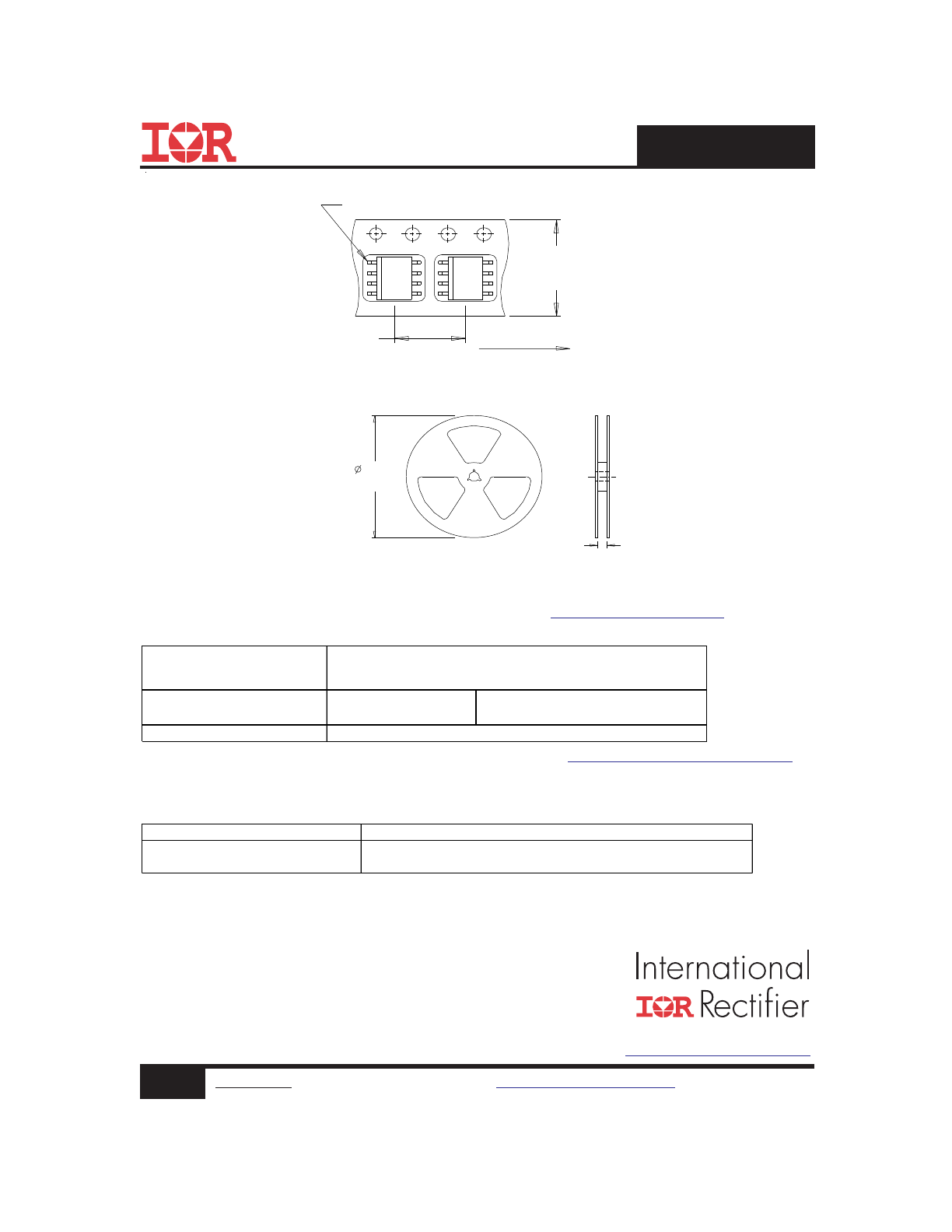
330.00
(12.992)
MAX.
14.40 ( .566 )
12.40 ( .488 )
NOTES :
1. CONTROLLING DIMENSION : MILLIMETER.
2. OUTLINE CONFORMS TO EIA-481 & EIA-541.
FEED DIRECTION
TERMINAL NUMBER 1
12.3 ( .484 )
11.7 ( .461 )
8.1 ( .318 )
7.9 ( .312 )
NOTES:
1. CONTROLLING DIMENSION : MILLIMETER.
2. ALL DIMENSIONS ARE SHOWN IN MILLIMETERS(INCHES).
3. OUTLINE CONFORMS TO EIA-481 & EIA-541.
SO-8 Tape and Reel
(Dimensions are shown in millimeters (inches))
IR WORLD HEADQUARTERS: 101 N. Sepulveda Blvd., El Segundo, California 90245, USA
To contact International Rectifier, please visit
http://www.irf.com/whoto-call/
† Qualification standards can be found at International Rectifier’s web site:
http://www.irf.com/product-info/reliability
††
Applicable version of JEDEC standard at the time of product release
MS L1
(per JEDEC J-S TD-020D
††
)
RoHS compliant
Yes
Qualification information
†
Qualification level
Consumer
(per JEDEC JES D47F
††
guidelines)
Moisture Sensitivity Level
SO-8
Note: For the most current drawing please refer to IR website at:
http://www.irf.com/package/
Date
Comments
• Added ordering information on page 1.
• Updated datasheet with new IR corporate template.
Revision History
10/29/2013