
www.irf.com
1
4/4/12
IRF6892STRPbF
IRF6892STR1PbF
DirectFET
®
plus MOSFET with Schottky Diode
Applicable DirectFET Outline and Substrate Outline
Typical values (unless otherwise specified)
ISOMETRIC
Description
The IRF6892SPbF combines the latest HEXFET® Power MOSFET Silicon technology with the advanced DirectFET
TM
packaging to achieve
the lowest on-state resistance in a package that has the footprint of a SO-8 and less than 0.7 mm profile. The DirectFET package is
compatible with existing layout geometries used in power applications, PCB assembly equipment and vapor phase, infra-red or convection
soldering techniques. Application note AN-1035 is followed regarding the manufacturing methods and processes. The DirectFET package
allows dual sided cooling to maximize thermal transfer in power systems, improving previous best thermal resistance by 80%.
The IRF6892SPbF balances industry leading on-state resistance while minimizing gate charge along with low gate resistance to reduce both
conduction and switching losses. This part contains an integrated Schottky diode to reduce the Qrr of the body drain diode further reducing
the losses in a Synchronous Buck circuit. The reduced losses make this product ideal for high frequency/high efficiency DC-DC converters
that power high current loads such as the latest generation of microprocessors. The IRF6892SPbF has been optimized for parameters that
are critical in synchronous buck converter’s Sync FET sockets.
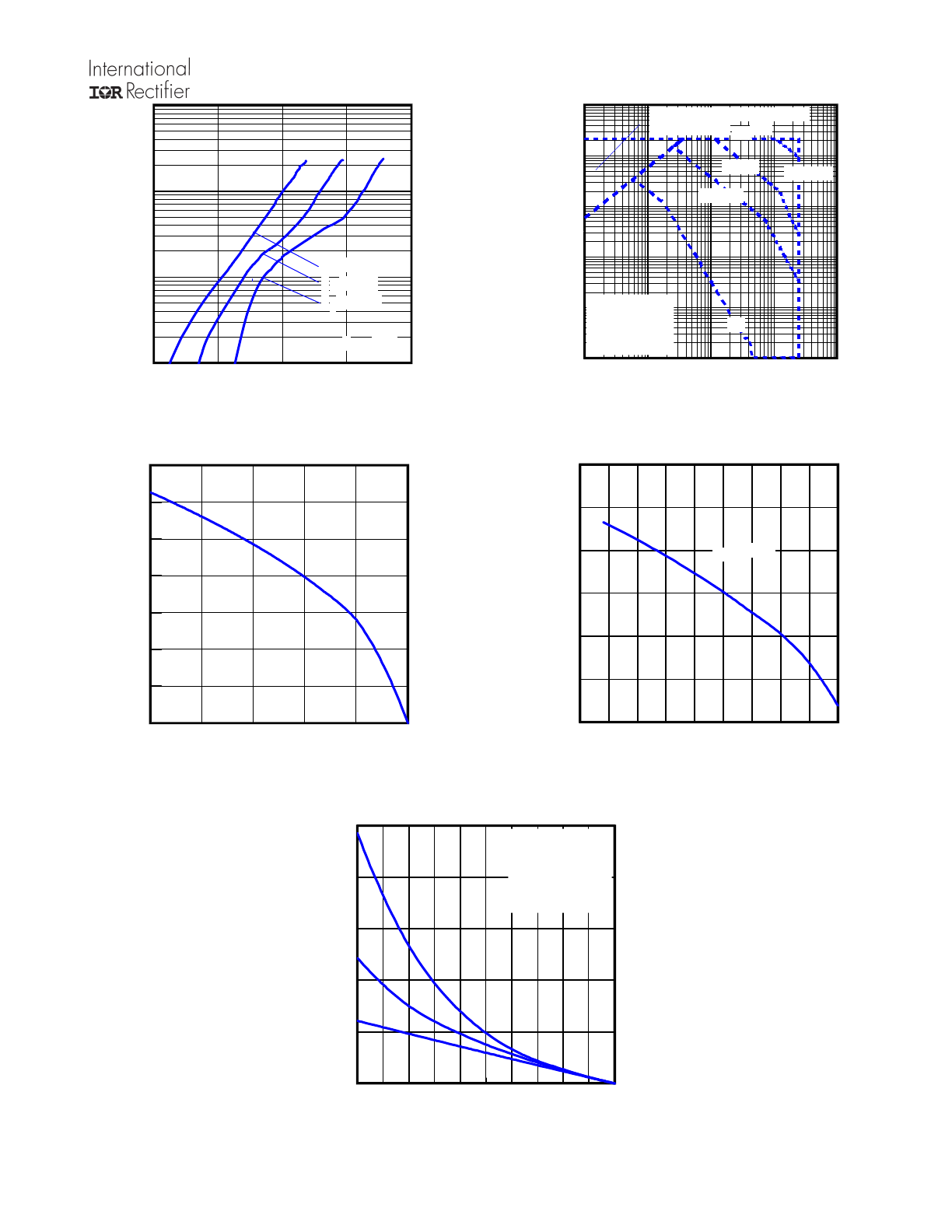
Fig 1. Typical On-Resistance vs. Gate Voltage
Fig 2. Typical Total Gate Charge vs Gate-to-Source Voltage
Click on this section to link to the appropriate technical paper.
Click on this section to link to the DirectFET Website.
Surface mounted on 1 in. square Cu board, steady state.
T
C
measured with thermocouple mounted to top (Drain) of part.
Repetitive rating; pulse width limited by max. junction temperature.
Starting T
J
= 25°C, L = 1.2mH, R
G
= 25
Ω, I
AS
= 22A.
Notes:
PD - 97770
S3C
l
RoHS Compliant and Halogen Free
l
Low Profile (<0.7 mm)
l
Dual Sided Cooling Compatible
l
Ultra Low Package Inductance
l
Optimized for High Frequency Switching
l
Ideal for CPU Core DC-DC Converters
l
Optimized for Control FET Application
l
Compatible with existing Surface Mount Techniques
l
100% Rg tested
Absolute Maximum Ratings
Parameter
Units
V
DS
Drain-to-Source Voltage
V
GS
Gate-to-Source Voltage
I
D
@ T
A
= 25°C
Continuous Drain Current, V
GS
@ 10V
e
I
D
@ T
A
= 70°C
Continuous Drain Current, V
GS
@ 10V
e
I
D
@ T
C
= 25°C
Continuous Drain Current, V
GS
@ 10V
f
I
DM
Pulsed Drain Current
g
E
AS
Single Pulse Avalanche Energy
h
mJ
I
AR
Avalanche Current
g
A
22
240
Max.
22
125
220
±16
25
28
V
A
D
G
D
S
S
S
S1
S2
S3C
M2 M4
L4
L6
L8
2
4
6
8
10
12
14
16
VGS, Gate -to -Source Voltage (V)
0.0
2.0
4.0
6.0
8.0
T
yp
ic
al
R
D
S
(o
n)
(
m
Ω
)
ID = 28A
TJ = 25°C
TJ = 125°C
0
10
20
30
40
50
QG Total Gate Charge (nC)
0.0
2.0
4.0
6.0
8.0
10.0
12.0
14.0
V
G
S
, G
at
e-
to
-S
ou
rc
e
V
ol
ta
ge
(
V
)
VDS= 20V
VDS= 13V
VDS= 5V
ID= 22A
Q
g tot
Q
gd
Q
gs2
Q
rr
Q
oss
V
gs(th)
17nC
6.0nC
2.3nC
39nC
16nC
1.8V
V
DSS
V
GS
R
DS(on)
R
DS(on)
25V max ±16V max 1.3mΩ @ 10V 2.0mΩ @ 4.5V
IRF6892STR/TR1PbF
2
www.irf.com
Notes:
Repetitive rating; pulse width limited by max. junction temperature.
Pulse width
≤ 400μs; duty cycle ≤ 2%.
D
S
G
Static @ T
J
= 25°C (unless otherwise specified)
Parameter
Min. Typ. Max. Units
BV
DSS
Drain-to-Source Breakdown Voltage
25
–––
–––
V
ΔΒV
DSS
/
ΔT
J
Breakdown Voltage Temp. Coefficient
–––
11
––– mV/°C
R
DS(on)
Static Drain-to-Source On-Resistance
–––
1.3
1.7
–––
2.0
2.6
V
GS(th)
Gate Threshold Voltage
1.1
1.8
2.1
V
ΔV
GS(th)
/ΔT
J
Gate Threshold Voltage Coefficient
–––
-9.8
––– mV/°C
I
DSS
Drain-to-Source Leakage Current
–––
–––
500
μA
–––
–––
5.0
mA
I
GSS
Gate-to-Source Forward Leakage
–––
–––
100
Gate-to-Source Reverse Leakage
–––
–––
-100
gfs
Forward Transconductance
290
–––
–––
S
Q
g
Total Gate Charge
–––
17
25
Q
gs1
Pre-Vth Gate-to-Source Charge
–––
4.0
–––
Q
gs2
Post-Vth Gate-to-Source Charge
–––
2.3
–––
Q
gd
Gate-to-Drain Charge
–––
6.0
–––
Q
godr
Gate Charge Overdrive
–––
4.7
–––
See Fig. 2 & 15
Q
sw
Switch Charge (Q
gs2
+ Q
gd
)
–––
8.3
–––
Q
oss
Output Charge
–––
16
–––
nC
R
G
Gate Resistance
–––
0.4
Ω
t
d(on)
Turn-On Delay Time
–––
12
–––
t
r
Rise Time
–––
30
–––
t
d(off)
Turn-Off Delay Time
–––
16
–––
t
f
Fall Time
–––
9.5
–––
C
iss
Input Capacitance
–––
2510
–––
C
oss
Output Capacitance
–––
850
–––
C
rss
Reverse Transfer Capacitance
–––
190
–––
Diode Characteristics
Parameter
Min. Typ. Max. Units
I
S
Continuous Source Current
(Body Diode)
A
I
SM
Pulsed Source Current
(Body Diode)
g
V
SD
Diode Forward Voltage
–––
–––
0.75
V
t
rr
Reverse Recovery Time
–––
22
33
ns
Q
rr
Reverse Recovery Charge
–––
37
56
nC
V
DS
= V
GS
, I
D
= 50μA
m
Ω
nA
nC
V
GS
= 4.5V, I
D
= 22A
i
–––
–––
–––
76
220
V
DS
= 13V
I
D
= 22A
MOSFET symbol
–––
ns
pF
V
GS
= 0V
di/dt = 300A/μs
i
T
J
= 25°C, I
S
= 22A, V
GS
= 0V
i
showing the
integral reverse
p-n junction diode.
T
J
= 25°C, I
F
= 22A
V
GS
= 16V
V
GS
= -16V
V
DS
= 20V, V
GS
= 0V
V
DS
= 13V
V
DS
= 20V, V
GS
= 0V, T
J
= 125°C
Conditions
V
GS
= 0V, I
D
= 1mA
Reference to 25°C, I
D
= 5mA
V
GS
= 10V, I
D
= 28A
i
R
G
= 1.8
Ω
V
DS
= 13V, I
D
= 22A
Conditions
ƒ = 1.0MHz
V
DS
= 10V, V
GS
= 0V
V
DD
= 13V, V
GS
= 4.5V
i
V
GS
= 4.5V
I
D
= 22A
IRF6892STR/TR1PbF
www.irf.com
3
Fig 3. Maximum Effective Transient Thermal Impedance, Junction-to-Ambient
Surface mounted on 1 in. square Cu board, steady state.
T
C
measured with thermocouple incontact with top (Drain) of part.
Used double sided cooling, mounting pad with large heatsink.
Notes:
Mounted on minimum footprint full size board with metalized
back and with small clip heatsink.
R
θ
is measured at
T
J
of approximately 90°C.
Surface mounted on 1 in. square Cu
board (still air).
Mounted on minimum footprint full size board with metalized
back and with small clip heatsink. (still air)
Absolute Maximum Ratings
Parameter
Units
P
D
@T
A
= 25°C
Power Dissipation
e
P
D
@T
A
= 70°C
Power Dissipation
e
P
D
@T
C
= 25°C
Power Dissipation
f
T
P
Peak Soldering Temperature
T
J
Operating Junction and
T
STG
Storage Temperature Range
Thermal Resistance
Parameter
Typ.
Max.
Units
R
θJA
Junction-to-Ambient
el
–––
60
R
θJA
Junction-to-Ambient
jl
12.5
–––
R
θJA
Junction-to-Ambient
kl
20
–––
°C/W
R
θJC
Junction-to-Case
fl
–––
3.0
R
θJ-PCB
Junction-to-PCB Mounted
1.0
–––
Linear Derating Factor
e
W/°C
0.016
270
-40 to + 150
Max.
42
2.1
1.3
W
°C
1E-006
1E-005
0.0001
0.001
0.01
0.1
1
10
100
t1 , Rectangular Pulse Duration (sec)
0.001
0.01
0.1
1
10
100
T
he
rm
al
R
es
po
ns
e
(
Z
th
JA
)
0.20
0.10
D = 0.50
0.02
0.01
0.05
SINGLE PULSE
( THERMAL RESPONSE )
Notes:
1. Duty Factor D = t1/t2
2. Peak Tj = P dm x Zthja + Tc
IRF6892STR/TR1PbF
4
www.irf.com
Fig 5. Typical Output Characteristics
Fig 4. Typical Output Characteristics
Fig 6. Typical Transfer Characteristics
Fig 7. Normalized On-Resistance vs. Temperature
Fig 8. Typical Capacitance vs.Drain-to-Source Voltage
Fig 9. Typical On-Resistance vs.
Drain Current and Gate Voltage
0.1
1
10
100
VDS, Drain-to-Source Voltage (V)
0.1
1
10
100
1000
I D
, D
ra
in
-t
o-
S
ou
rc
e
C
ur
re
nt
(
A
)
VGS
TOP
10V
4.5V
3.5V
3.2V
2.9V
2.7V
2.6V
BOTTOM
2.4V
≤60μs PULSE WIDTH
Tj = 25°C
2.5V
0.1
1
10
100
VDS, Drain-to-Source Voltage (V)
1
10
100
1000
I D
, D
ra
in
-t
o-
S
ou
rc
e
C
ur
re
nt
(
A
)
VGS
TOP
10V
4.5V
3.5V
3.2V
2.9V
2.7V
2.6V
BOTTOM
2.4V
≤60μs PULSE WIDTH
Tj = 150°C
2.5V
1
2
3
4
VGS, Gate-to-Source Voltage (V)
0.1
1
10
100
1000
I D
, D
ra
in
-t
o-
S
ou
rc
e
C
ur
re
nt
(
A
)
TJ = 150°C
TJ = 25°C
TJ = -40°C
VDS = 15V
≤60μs PULSE WIDTH
-60 -40 -20 0 20 40 60 80 100 120 140 160
TJ , Junction Temperature (°C)
0.5
1.0
1.5
2.0
T
yp
ic
al
R
D
S
(o
n)
(
N
or
m
al
iz
ed
)
ID = 28A
VGS = 10V
VGS = 4.5V
1
10
100
VDS, Drain-to-Source Voltage (V)
100
1000
10000
100000
C
, C
ap
ac
ita
nc
e(
pF
)
VGS = 0V, f = 1 MHZ
Ciss = Cgs + Cgd, C ds SHORTED
Crss = Cgd
Coss = Cds + Cgd
Coss
Crss
Ciss
0
20
40
60
80 100 120 140 160 180
ID, Drain Current (A)
0
2
4
6
8
10
12
14
T
yp
ic
al
R
D
S
(o
n)
(
m
Ω
)
TJ = 25°C
Vgs = 3.5V
Vgs = 4.0V
Vgs = 4.5V
Vgs = 5.0V
Vgs = 10V
IRF6892STR/TR1PbF
www.irf.com
5
Fig 13. Typical Threshold Voltage vs. Junction
Temperature
Fig 12. Maximum Drain Current vs. Case Temperature
Fig 10. Typical Source-Drain Diode Forward Voltage
Fig 11. Maximum Safe Operating Area
Fig 14. Maximum Avalanche Energy vs. Drain Current
0.2
0.4
0.6
0.8
1.0
VSD, Source-to-Drain Voltage (V)
1
10
100
1000
I S
D
, R
ev
er
se
D
ra
in
C
ur
re
nt
(
A
)
TJ = 150°C
TJ = 25°C
TJ = -40°C
VGS = 0V
25
50
75
100
125
150
TC , Case Temperature (°C)
0
20
40
60
80
100
120
140
I D
,
D
ra
in
C
ur
re
nt
(
A
)
-75 -50 -25
0
25
50
75 100 125 150
TJ , Temperature ( °C )
1.0
1.5
2.0
2.5
T
yp
ic
al
V
G
S
(t
h)
G
at
e
th
re
sh
ol
d
V
ol
ta
ge
(
V
)
ID = 1.0mA
25
50
75
100
125
150
Starting TJ , Junction Temperature (°C)
0
200
400
600
800
1000
E
A
S
,
S
in
gl
e
P
ul
se
A
va
la
nc
he
E
ne
rg
y
(m
J)
ID
TOP 1.3A
2.1A
BOTTOM 22A
0.01
0.1
1
10
100
VDS , Drain-toSource Voltage (V)
0.01
0.1
1
10
100
1000
I D
,
D
ra
in
-t
o-
S
ou
rc
e
C
ur
re
nt
(
A
)
TA = 25°C
Tj = 150°C
Single Pulse
1msec
10msec
OPERATION IN THIS AREA
LIMITED BY R DS(on)
100μsec
DC
IRF6892STR/TR1PbF
6
www.irf.com
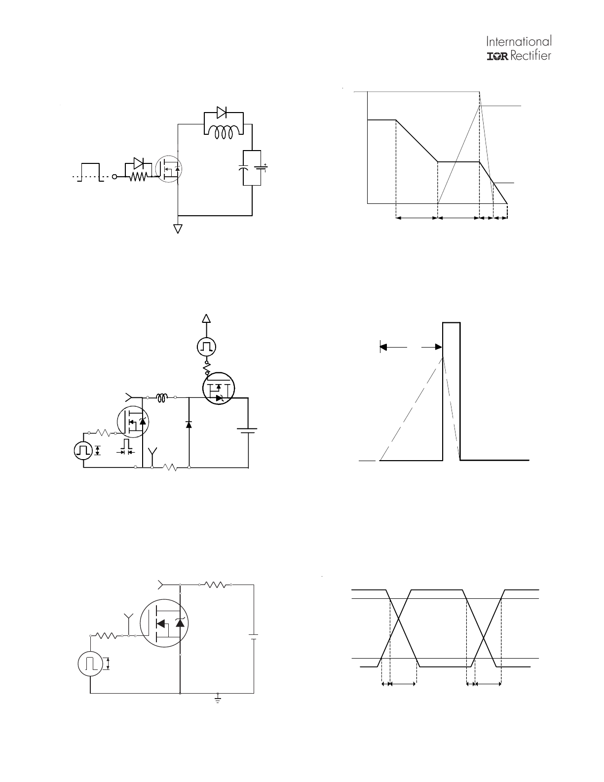
Fig 15a. Gate Charge Test Circuit
Fig 15b. Gate Charge Waveform
Fig 16b. Unclamped Inductive Waveforms
Fig 16a. Unclamped Inductive Test Circuit
Fig 17b. Switching Time Waveforms
Fig 17a. Switching Time Test Circuit
1K
VCC
DUT
0
L
S
20K
Vds
Vgs
Id
Vgs(th)
Qgs1
Qgs2
Qgd
Qgodr
R G
IAS
0.01
Ω
tp
D.U.T
L
VDS
+
- VDD
DRIVER
A
15V
20V
tp
V
(BR)DSS
I
AS
V
DS
Pulse Width ≤ 1 µs
Duty Factor ≤ 0.1 %
R
D
V
GS
R
G
D.U.T.
10V
+
-
V
DD
V
GS
V
DS
V
GS
90%
10%
t
d(off)
t
d(on)
t
f
t
r
IRF6892STR/TR1PbF
www.irf.com
7
Fig 19.
Diode Reverse Recovery Test Circuit for N-Channel
HEXFET
®
Power MOSFETs
P.W.
Period
di/dt
Diode Recovery
dv/dt
Ripple
≤ 5%
Body Diode Forward Drop
Re-Applied
Voltage
Reverse
Recovery
Current
Body Diode Forward
Current
V
GS
=10V
V
DD
I
SD
Driver Gate Drive
D.U.T. I
SD
Waveform
D.U.T. V
DS
Waveform
Inductor Curent
D =
P.W.
Period
*
V
GS
= 5V for Logic Level Devices
*
Inductor Current
Circuit Layout Considerations
• Low Stray Inductance
• Ground Plane
• Low Leakage Inductance
Current Transformer
• di/dt controlled by R
G
• Driver same type as D.U.T.
• I
SD
controlled by Duty Factor "D"
• D.U.T. - Device Under Test
+
-
+
+
+
-
-
-
R
G
V
DD
D.U.T
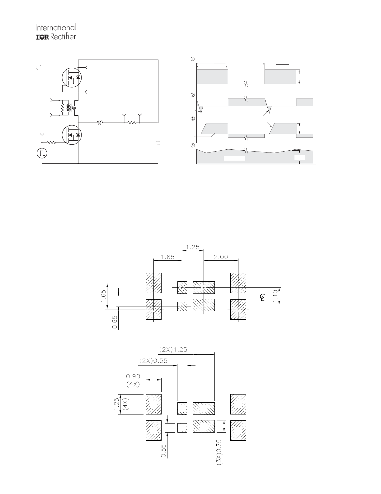
DirectFET
®
plus
Board Footprint, S3C (Small Size Can).
Please see AN-1035 for DirectFET assembly details and stencil and substrate design recommendations
D
D
D
D
G=GATE
D=DRAIN
S=SOURCE
G
S
S
S
IRF6892STR/TR1PbF
8
www.irf.com
DirectFET
®
plus
Part Marking
DirectFET
®
plus
Outline Dimension, S3C Outline (Small Size Can).
Please see AN-1035 for DirectFET assembly details and stencil and substrate design recommendations
GATE MARKING
PART NUMBER
LOGO
BATCH NUMBER
DATE CODE
Line above the last character of
the date code indicates "Lead-Free"
CODE
A
B
C
D
E
F
G
H
J
K
L
M
R
P
0.016
0.0031
0.007
0.039
0.075
0.112
0.018
0.020
MAX
0.191
0.156
0.38
0.02
0.08
0.90
1.80
2.75
0.35
0.48
MIN
4.75
3.70
0.42
0.08
0.17
1.00
1.90
2.85
0.45
0.52
MAX
4.85
3.95
0.015
0.003
0.0008
0.071
0.035
0.108
0.019
0.014
MIN
0.146
0.187
METRIC
IMPERIAL
DIMENSIONS
1.18
1.22
0.048
0.047
0.028
0.68
0.72
0.027
0.024
0.52
0.62
0.020
0.020
0.48
0.52
0.019
IRF6892STR/TR1PbF
www.irf.com
9
Data and specifications subject to change without notice.
This product has been designed and qualified to MSL1 rating for the Consumer market.
Additional storage requirement details for DirectFET products can be found in application note AN1035 on IRs Web site.
Qualification Standards can be found on IR’s Web site.
IR WORLD HEADQUARTERS: 233 Kansas St., El Segundo, California 90245, USA Tel: (310) 252-7105
TAC Fax: (310) 252-7903
Visit us at www.irf.com for sales contact information.04/2012
DirectFET
®
plus
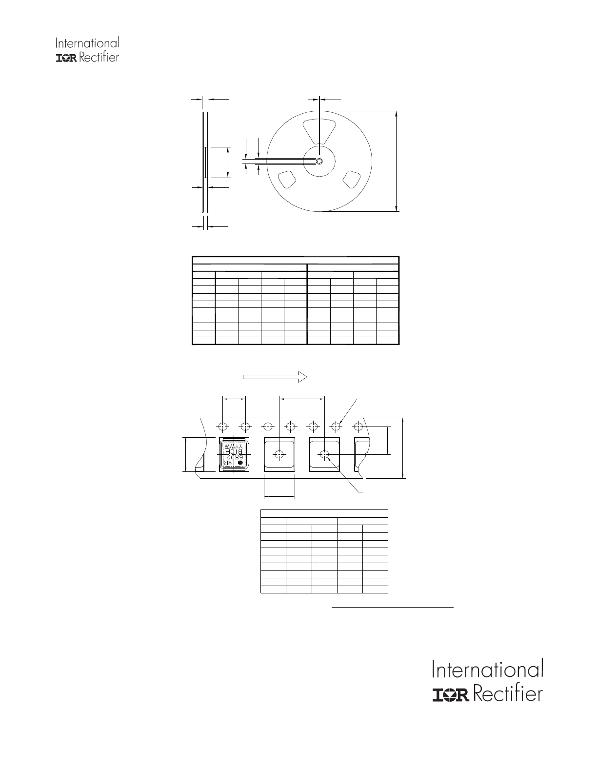
Tape & Reel Dimension (Showing component orientation).
REEL DIMENSIONS
NOTE: Controlling dimensions in mm
Std reel quantity is 4800 parts. (ordered as IRF6892STRPBF). For 1000 parts on 7"
reel, order IRF6892STR1PBF
B
C
MAX
N.C
N.C
0.520
N.C
N.C
0.724
0.567
0.606
IMPERIAL
H
MIN
330.0
20.2
12.8
1.5
100.0
N.C
12.4
11.9
STANDARD OPTION (QTY 4800)
CODE
A
B
C
D
E
F
G
H
MAX
N.C
N.C
13.2
N.C
N.C
18.4
14.4
15.4
MIN
12.992
0.795
0.504
0.059
3.937
N.C
0.488
0.469
METRIC
G
E
F
MIN
6.9
0.75
0.53
0.059
2.31
N.C
0.47
0.47
TR1 OPTION (QTY 1000)
MAX
N.C
N.C
12.8
N.C
N.C
13.50
12.01
12.01
MIN
177.77
19.06
13.5
1.5
58.72
N.C
11.9
11.9
METRIC
MAX
N.C
N.C
0.50
N.C
N.C
0.53
N.C
N.C
IMPERIAL
A
D
LOADED TAPE FEED DIRECTION
A
E
NOTE: C ON TROLLING
DIMEN SION S IN MM
C OD E
A
B
C
D
E
F
G
H
F
B
C
IMPERIAL
MIN
0.311
0.154
0.469
0.215
0.158
0.197
0.059
0.059
MAX
8.10
4.10
12.30
5.55
4.20
5.20
N.C
1.60
MIN
7.90
3.90
11.90
5.45
4.00
5.00
1.50
1.50
METR IC
DIMEN SIONS
MAX
0.319
0.161
0.484
0.219
0.165
0.205
N.C
0.063
D
H
G
Note: For the most current drawing please refer to IR website at
http://www.irf.com/package
www.irf.com
1
4/4/12
IRF6892STRPbF
IRF6892STR1PbF
DirectFET
®
plus MOSFET with Schottky Diode
Applicable DirectFET Outline and Substrate Outline
Typical values (unless otherwise specified)
ISOMETRIC
Description
The IRF6892SPbF combines the latest HEXFET® Power MOSFET Silicon technology with the advanced DirectFET
TM
packaging to achieve
the lowest on-state resistance in a package that has the footprint of a SO-8 and less than 0.7 mm profile. The DirectFET package is
compatible with existing layout geometries used in power applications, PCB assembly equipment and vapor phase, infra-red or convection
soldering techniques. Application note AN-1035 is followed regarding the manufacturing methods and processes. The DirectFET package
allows dual sided cooling to maximize thermal transfer in power systems, improving previous best thermal resistance by 80%.
The IRF6892SPbF balances industry leading on-state resistance while minimizing gate charge along with low gate resistance to reduce both
conduction and switching losses. This part contains an integrated Schottky diode to reduce the Qrr of the body drain diode further reducing
the losses in a Synchronous Buck circuit. The reduced losses make this product ideal for high frequency/high efficiency DC-DC converters
that power high current loads such as the latest generation of microprocessors. The IRF6892SPbF has been optimized for parameters that
are critical in synchronous buck converter’s Sync FET sockets.
Fig 1. Typical On-Resistance vs. Gate Voltage
Fig 2. Typical Total Gate Charge vs Gate-to-Source Voltage
Click on this section to link to the appropriate technical paper.
Click on this section to link to the DirectFET Website.
Surface mounted on 1 in. square Cu board, steady state.
T
C
measured with thermocouple mounted to top (Drain) of part.
Repetitive rating; pulse width limited by max. junction temperature.
Starting T
J
= 25°C, L = 1.2mH, R
G
= 25
Ω, I
AS
= 22A.
Notes:
PD - 97770
S3C
l
RoHS Compliant and Halogen Free
l
Low Profile (<0.7 mm)
l
Dual Sided Cooling Compatible
l
Ultra Low Package Inductance
l
Optimized for High Frequency Switching
l
Ideal for CPU Core DC-DC Converters
l
Optimized for Control FET Application
l
Compatible with existing Surface Mount Techniques
l
100% Rg tested
Absolute Maximum Ratings
Parameter
Units
V
DS
Drain-to-Source Voltage
V
GS
Gate-to-Source Voltage
I
D
@ T
A
= 25°C
Continuous Drain Current, V
GS
@ 10V
e
I
D
@ T
A
= 70°C
Continuous Drain Current, V
GS
@ 10V
e
I
D
@ T
C
= 25°C
Continuous Drain Current, V
GS
@ 10V
f
I
DM
Pulsed Drain Current
g
E
AS
Single Pulse Avalanche Energy
h
mJ
I
AR
Avalanche Current
g
A
22
240
Max.
22
125
220
±16
25
28
V
A
D
G
D
S
S
S
S1
S2
S3C
M2 M4
L4
L6
L8
2
4
6
8
10
12
14
16
VGS, Gate -to -Source Voltage (V)
0.0
2.0
4.0
6.0
8.0
T
yp
ic
al
R
D
S
(o
n)
(
m
Ω
)
ID = 28A
TJ = 25°C
TJ = 125°C
0
10
20
30
40
50
QG Total Gate Charge (nC)
0.0
2.0
4.0
6.0
8.0
10.0
12.0
14.0
V
G
S
, G
at
e-
to
-S
ou
rc
e
V
ol
ta
ge
(
V
)
VDS= 20V
VDS= 13V
VDS= 5V
ID= 22A
Q
g tot
Q
gd
Q
gs2
Q
rr
Q
oss
V
gs(th)
17nC
6.0nC
2.3nC
39nC
16nC
1.8V
V
DSS
V
GS
R
DS(on)
R
DS(on)
25V max ±16V max 1.3mΩ @ 10V 2.0mΩ @ 4.5V
IRF6892STR/TR1PbF
2
www.irf.com
Notes:
Repetitive rating; pulse width limited by max. junction temperature.
Pulse width
≤ 400μs; duty cycle ≤ 2%.
D
S
G
Static @ T
J
= 25°C (unless otherwise specified)
Parameter
Min. Typ. Max. Units
BV
DSS
Drain-to-Source Breakdown Voltage
25
–––
–––
V
ΔΒV
DSS
/
ΔT
J
Breakdown Voltage Temp. Coefficient
–––
11
––– mV/°C
R
DS(on)
Static Drain-to-Source On-Resistance
–––
1.3
1.7
–––
2.0
2.6
V
GS(th)
Gate Threshold Voltage
1.1
1.8
2.1
V
ΔV
GS(th)
/ΔT
J
Gate Threshold Voltage Coefficient
–––
-9.8
––– mV/°C
I
DSS
Drain-to-Source Leakage Current
–––
–––
500
μA
–––
–––
5.0
mA
I
GSS
Gate-to-Source Forward Leakage
–––
–––
100
Gate-to-Source Reverse Leakage
–––
–––
-100
gfs
Forward Transconductance
290
–––
–––
S
Q
g
Total Gate Charge
–––
17
25
Q
gs1
Pre-Vth Gate-to-Source Charge
–––
4.0
–––
Q
gs2
Post-Vth Gate-to-Source Charge
–––
2.3
–––
Q
gd
Gate-to-Drain Charge
–––
6.0
–––
Q
godr
Gate Charge Overdrive
–––
4.7
–––
See Fig. 2 & 15
Q
sw
Switch Charge (Q
gs2
+ Q
gd
)
–––
8.3
–––
Q
oss
Output Charge
–––
16
–––
nC
R
G
Gate Resistance
–––
0.4
Ω
t
d(on)
Turn-On Delay Time
–––
12
–––
t
r
Rise Time
–––
30
–––
t
d(off)
Turn-Off Delay Time
–––
16
–––
t
f
Fall Time
–––
9.5
–––
C
iss
Input Capacitance
–––
2510
–––
C
oss
Output Capacitance
–––
850
–––
C
rss
Reverse Transfer Capacitance
–––
190
–––
Diode Characteristics
Parameter
Min. Typ. Max. Units
I
S
Continuous Source Current
(Body Diode)
A
I
SM
Pulsed Source Current
(Body Diode)
g
V
SD
Diode Forward Voltage
–––
–––
0.75
V
t
rr
Reverse Recovery Time
–––
22
33
ns
Q
rr
Reverse Recovery Charge
–––
37
56
nC
V
DS
= V
GS
, I
D
= 50μA
m
Ω
nA
nC
V
GS
= 4.5V, I
D
= 22A
i
–––
–––
–––
76
220
V
DS
= 13V
I
D
= 22A
MOSFET symbol
–––
ns
pF
V
GS
= 0V
di/dt = 300A/μs
i
T
J
= 25°C, I
S
= 22A, V
GS
= 0V
i
showing the
integral reverse
p-n junction diode.
T
J
= 25°C, I
F
= 22A
V
GS
= 16V
V
GS
= -16V
V
DS
= 20V, V
GS
= 0V
V
DS
= 13V
V
DS
= 20V, V
GS
= 0V, T
J
= 125°C
Conditions
V
GS
= 0V, I
D
= 1mA
Reference to 25°C, I
D
= 5mA
V
GS
= 10V, I
D
= 28A
i
R
G
= 1.8
Ω
V
DS
= 13V, I
D
= 22A
Conditions
ƒ = 1.0MHz
V
DS
= 10V, V
GS
= 0V
V
DD
= 13V, V
GS
= 4.5V
i
V
GS
= 4.5V
I
D
= 22A
IRF6892STR/TR1PbF
www.irf.com
3
Fig 3. Maximum Effective Transient Thermal Impedance, Junction-to-Ambient
Surface mounted on 1 in. square Cu board, steady state.
T
C
measured with thermocouple incontact with top (Drain) of part.
Used double sided cooling, mounting pad with large heatsink.
Notes:
Mounted on minimum footprint full size board with metalized
back and with small clip heatsink.
R
θ
is measured at
T
J
of approximately 90°C.
Surface mounted on 1 in. square Cu
board (still air).
Mounted on minimum footprint full size board with metalized
back and with small clip heatsink. (still air)
Absolute Maximum Ratings
Parameter
Units
P
D
@T
A
= 25°C
Power Dissipation
e
P
D
@T
A
= 70°C
Power Dissipation
e
P
D
@T
C
= 25°C
Power Dissipation
f
T
P
Peak Soldering Temperature
T
J
Operating Junction and
T
STG
Storage Temperature Range
Thermal Resistance
Parameter
Typ.
Max.
Units
R
θJA
Junction-to-Ambient
el
–––
60
R
θJA
Junction-to-Ambient
jl
12.5
–––
R
θJA
Junction-to-Ambient
kl
20
–––
°C/W
R
θJC
Junction-to-Case
fl
–––
3.0
R
θJ-PCB
Junction-to-PCB Mounted
1.0
–––
Linear Derating Factor
e
W/°C
0.016
270
-40 to + 150
Max.
42
2.1
1.3
W
°C
1E-006
1E-005
0.0001
0.001
0.01
0.1
1
10
100
t1 , Rectangular Pulse Duration (sec)
0.001
0.01
0.1
1
10
100
T
he
rm
al
R
es
po
ns
e
(
Z
th
JA
)
0.20
0.10
D = 0.50
0.02
0.01
0.05
SINGLE PULSE
( THERMAL RESPONSE )
Notes:
1. Duty Factor D = t1/t2
2. Peak Tj = P dm x Zthja + Tc
IRF6892STR/TR1PbF
4
www.irf.com
Fig 5. Typical Output Characteristics
Fig 4. Typical Output Characteristics
Fig 6. Typical Transfer Characteristics
Fig 7. Normalized On-Resistance vs. Temperature
Fig 8. Typical Capacitance vs.Drain-to-Source Voltage
Fig 9. Typical On-Resistance vs.
Drain Current and Gate Voltage
0.1
1
10
100
VDS, Drain-to-Source Voltage (V)
0.1
1
10
100
1000
I D
, D
ra
in
-t
o-
S
ou
rc
e
C
ur
re
nt
(
A
)
VGS
TOP
10V
4.5V
3.5V
3.2V
2.9V
2.7V
2.6V
BOTTOM
2.4V
≤60μs PULSE WIDTH
Tj = 25°C
2.5V
0.1
1
10
100
VDS, Drain-to-Source Voltage (V)
1
10
100
1000
I D
, D
ra
in
-t
o-
S
ou
rc
e
C
ur
re
nt
(
A
)
VGS
TOP
10V
4.5V
3.5V
3.2V
2.9V
2.7V
2.6V
BOTTOM
2.4V
≤60μs PULSE WIDTH
Tj = 150°C
2.5V
1
2
3
4
VGS, Gate-to-Source Voltage (V)
0.1
1
10
100
1000
I D
, D
ra
in
-t
o-
S
ou
rc
e
C
ur
re
nt
(
A
)
TJ = 150°C
TJ = 25°C
TJ = -40°C
VDS = 15V
≤60μs PULSE WIDTH
-60 -40 -20 0 20 40 60 80 100 120 140 160
TJ , Junction Temperature (°C)
0.5
1.0
1.5
2.0
T
yp
ic
al
R
D
S
(o
n)
(
N
or
m
al
iz
ed
)
ID = 28A
VGS = 10V
VGS = 4.5V
1
10
100
VDS, Drain-to-Source Voltage (V)
100
1000
10000
100000
C
, C
ap
ac
ita
nc
e(
pF
)
VGS = 0V, f = 1 MHZ
Ciss = Cgs + Cgd, C ds SHORTED
Crss = Cgd
Coss = Cds + Cgd
Coss
Crss
Ciss
0
20
40
60
80 100 120 140 160 180
ID, Drain Current (A)
0
2
4
6
8
10
12
14
T
yp
ic
al
R
D
S
(o
n)
(
m
Ω
)
TJ = 25°C
Vgs = 3.5V
Vgs = 4.0V
Vgs = 4.5V
Vgs = 5.0V
Vgs = 10V
IRF6892STR/TR1PbF
www.irf.com
5
Fig 13. Typical Threshold Voltage vs. Junction
Temperature
Fig 12. Maximum Drain Current vs. Case Temperature
Fig 10. Typical Source-Drain Diode Forward Voltage
Fig 11. Maximum Safe Operating Area
Fig 14. Maximum Avalanche Energy vs. Drain Current
0.2
0.4
0.6
0.8
1.0
VSD, Source-to-Drain Voltage (V)
1
10
100
1000
I S
D
, R
ev
er
se
D
ra
in
C
ur
re
nt
(
A
)
TJ = 150°C
TJ = 25°C
TJ = -40°C
VGS = 0V
25
50
75
100
125
150
TC , Case Temperature (°C)
0
20
40
60
80
100
120
140
I D
,
D
ra
in
C
ur
re
nt
(
A
)
-75 -50 -25
0
25
50
75 100 125 150
TJ , Temperature ( °C )
1.0
1.5
2.0
2.5
T
yp
ic
al
V
G
S
(t
h)
G
at
e
th
re
sh
ol
d
V
ol
ta
ge
(
V
)
ID = 1.0mA
25
50
75
100
125
150
Starting TJ , Junction Temperature (°C)
0
200
400
600
800
1000
E
A
S
,
S
in
gl
e
P
ul
se
A
va
la
nc
he
E
ne
rg
y
(m
J)
ID
TOP 1.3A
2.1A
BOTTOM 22A
0.01
0.1
1
10
100
VDS , Drain-toSource Voltage (V)
0.01
0.1
1
10
100
1000
I D
,
D
ra
in
-t
o-
S
ou
rc
e
C
ur
re
nt
(
A
)
TA = 25°C
Tj = 150°C
Single Pulse
1msec
10msec
OPERATION IN THIS AREA
LIMITED BY R DS(on)
100μsec
DC
IRF6892STR/TR1PbF
6
www.irf.com
Fig 15a. Gate Charge Test Circuit
Fig 15b. Gate Charge Waveform
Fig 16b. Unclamped Inductive Waveforms
Fig 16a. Unclamped Inductive Test Circuit
Fig 17b. Switching Time Waveforms
Fig 17a. Switching Time Test Circuit
1K
VCC
DUT
0
L
S
20K
Vds
Vgs
Id
Vgs(th)
Qgs1
Qgs2
Qgd
Qgodr
R G
IAS
0.01
Ω
tp
D.U.T
L
VDS
+
- VDD
DRIVER
A
15V
20V
tp
V
(BR)DSS
I
AS
V
DS
Pulse Width ≤ 1 µs
Duty Factor ≤ 0.1 %
R
D
V
GS
R
G
D.U.T.
10V
+
-
V
DD
V
GS
V
DS
V
GS
90%
10%
t
d(off)
t
d(on)
t
f
t
r
IRF6892STR/TR1PbF
www.irf.com
7
Fig 19.
Diode Reverse Recovery Test Circuit for N-Channel
HEXFET
®
Power MOSFETs
P.W.
Period
di/dt
Diode Recovery
dv/dt
Ripple
≤ 5%
Body Diode Forward Drop
Re-Applied
Voltage
Reverse
Recovery
Current
Body Diode Forward
Current
V
GS
=10V
V
DD
I
SD
Driver Gate Drive
D.U.T. I
SD
Waveform
D.U.T. V
DS
Waveform
Inductor Curent
D =
P.W.
Period
*
V
GS
= 5V for Logic Level Devices
*
Inductor Current
Circuit Layout Considerations
• Low Stray Inductance
• Ground Plane
• Low Leakage Inductance
Current Transformer
• di/dt controlled by R
G
• Driver same type as D.U.T.
• I
SD
controlled by Duty Factor "D"
• D.U.T. - Device Under Test
+
-
+
+
+
-
-
-
R
G
V
DD
D.U.T
DirectFET
®
plus
Board Footprint, S3C (Small Size Can).
Please see AN-1035 for DirectFET assembly details and stencil and substrate design recommendations
D
D
D
D
G=GATE
D=DRAIN
S=SOURCE
G
S
S
S
IRF6892STR/TR1PbF
8
www.irf.com
DirectFET
®
plus
Part Marking
DirectFET
®
plus
Outline Dimension, S3C Outline (Small Size Can).
Please see AN-1035 for DirectFET assembly details and stencil and substrate design recommendations
GATE MARKING
PART NUMBER
LOGO
BATCH NUMBER
DATE CODE
Line above the last character of
the date code indicates "Lead-Free"
CODE
A
B
C
D
E
F
G
H
J
K
L
M
R
P
0.016
0.0031
0.007
0.039
0.075
0.112
0.018
0.020
MAX
0.191
0.156
0.38
0.02
0.08
0.90
1.80
2.75
0.35
0.48
MIN
4.75
3.70
0.42
0.08
0.17
1.00
1.90
2.85
0.45
0.52
MAX
4.85
3.95
0.015
0.003
0.0008
0.071
0.035
0.108
0.019
0.014
MIN
0.146
0.187
METRIC
IMPERIAL
DIMENSIONS
1.18
1.22
0.048
0.047
0.028
0.68
0.72
0.027
0.024
0.52
0.62
0.020
0.020
0.48
0.52
0.019
IRF6892STR/TR1PbF
www.irf.com
9
Data and specifications subject to change without notice.
This product has been designed and qualified to MSL1 rating for the Consumer market.
Additional storage requirement details for DirectFET products can be found in application note AN1035 on IRs Web site.
Qualification Standards can be found on IR’s Web site.
IR WORLD HEADQUARTERS: 233 Kansas St., El Segundo, California 90245, USA Tel: (310) 252-7105
TAC Fax: (310) 252-7903
Visit us at www.irf.com for sales contact information.04/2012
DirectFET
®
plus
Tape & Reel Dimension (Showing component orientation).
REEL DIMENSIONS
NOTE: Controlling dimensions in mm
Std reel quantity is 4800 parts. (ordered as IRF6892STRPBF). For 1000 parts on 7"
reel, order IRF6892STR1PBF
B
C
MAX
N.C
N.C
0.520
N.C
N.C
0.724
0.567
0.606
IMPERIAL
H
MIN
330.0
20.2
12.8
1.5
100.0
N.C
12.4
11.9
STANDARD OPTION (QTY 4800)
CODE
A
B
C
D
E
F
G
H
MAX
N.C
N.C
13.2
N.C
N.C
18.4
14.4
15.4
MIN
12.992
0.795
0.504
0.059
3.937
N.C
0.488
0.469
METRIC
G
E
F
MIN
6.9
0.75
0.53
0.059
2.31
N.C
0.47
0.47
TR1 OPTION (QTY 1000)
MAX
N.C
N.C
12.8
N.C
N.C
13.50
12.01
12.01
MIN
177.77
19.06
13.5
1.5
58.72
N.C
11.9
11.9
METRIC
MAX
N.C
N.C
0.50
N.C
N.C
0.53
N.C
N.C
IMPERIAL
A
D
LOADED TAPE FEED DIRECTION
A
E
NOTE: C ON TROLLING
DIMEN SION S IN MM
C OD E
A
B
C
D
E
F
G
H
F
B
C
IMPERIAL
MIN
0.311
0.154
0.469
0.215
0.158
0.197
0.059
0.059
MAX
8.10
4.10
12.30
5.55
4.20
5.20
N.C
1.60
MIN
7.90
3.90
11.90
5.45
4.00
5.00
1.50
1.50
METR IC
DIMEN SIONS
MAX
0.319
0.161
0.484
0.219
0.165
0.205
N.C
0.063
D
H
G
Note: For the most current drawing please refer to IR website at
http://www.irf.com/package