
Notes
through
are on page 2
Applicable DirectFET Outline and Substrate Outline (see p. 6, 7 for details)
Description
This Digital Audio MOSFET is specifically designed for Class-D audio amplifier applications. This MOSFET utilizes the
latest processing techniques to achieve low on-resistance per silicon area. Furthermore, gate charge, body-diode reverse
recovery and internal gate resistance are optimized to improve key Class-D audio amplifier performance factors such as
efficiency, THD, and EMI.
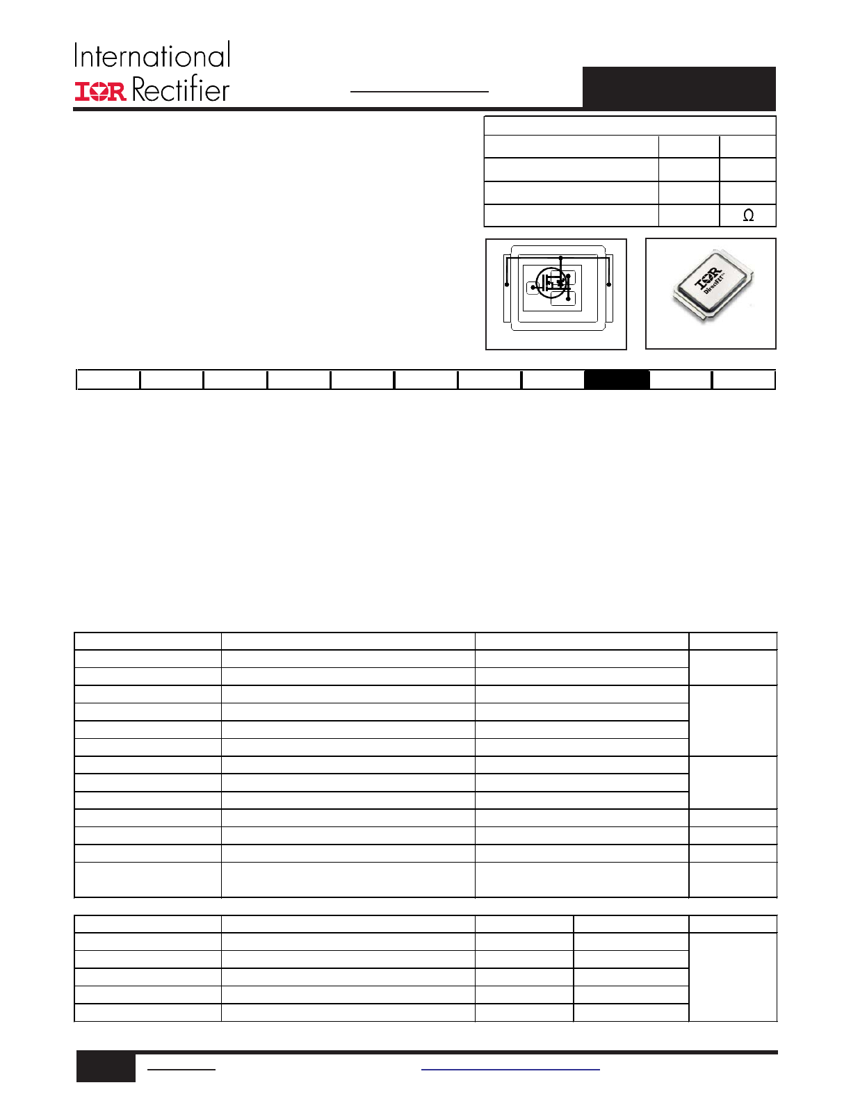
The IRF6775MPbF device utilizes DirectFET
TM
packaging technology. DirectFET
TM
packaging technology offers lower parasitic
inductance and resistance when compared to conventional wirebonded SOIC packaging. Lower inductance improves EMI
performance by reducing the voltage ringing that accompanies fast current transients. The DirectFET
TM
package is compatible
with existing layout geometries used in power applications, PCB assembly equipment and vapor phase, infra-red or convection
soldering techniques, when application note AN-1035 is followed regarding the manufacturing method and processes. The
DirectFET
TM
package also allows dual sided cooling to maximize thermal transfer in power systems, improving thermal resis-
tance and power dissipation. These features combine to make this MOSFET a highly efficient, robust and reliable device for
Class-D audio amplifier applications.
Features
• Latest MOSFET Silicon technology
• Key parameters optimized for Class-D audio amplifier
applications
• Low R
DS(on)
for improved efficiency
• Low Q
g
for better THD and improved efficiency
• Low Q
rr
for better THD and lower EMI
• Low package stray inductance for reduced ringing and lower EMI
• Can deliver up to 250W per channel into 4Ω Load in
Half-Bridge Configuration Amplifier
• Dual sided cooling compatible
· Compatible with existing surface mount technologies
· RoHS compliant containing no lead or bromide
·Lead-Free (Qualified up to 260°C Reflow)
DirectFET
ISOMETRIC
MZ
SQ
SX
ST
SH
MQ
MX
MT
MN
MZ
&
)
5
5
&
V
DS
150
V
R
DS(on)
typ. @ V
GS
= 10V
47
m
:
Q
g
typ.
25.0
nC
R
G(int)
max.
3.0
Key Parameters
Absolute Maximum Ratings
Parameter
Units
V
DS
Drain-to-Source Voltage
V
V
GS
Gate-to-Source Voltage
I
D
@ T
C
= 25°C
Continuous Drain Current, V
GS
@ 10V
I
D
@ T
A
= 25°C
Continuous Drain Current, V
GS
@ 10V
A
I
D
@ T
A
= 70°C
Continuous Drain Current, V
GS
@ 10V
I
DM
Pulsed Drain Current
c
P
D
@T
C
= 25°C
Maximum Power Dissipation
W
P
D
@T
A
= 25°C
Power Dissipation
e
P
D
@T
A
= 70°C
Power Dissipation
e
E
AS
Single Pulse Avalanche Energy
d
mJ
I
AR
Avalanche Current
c
A
Linear Derating Factor
e
W/°C
T
J
Operating Junction and
°C
T
STG
Storage Temperature Range
Thermal Resistance
Parameter
Typ.
Max.
Units
R
θJA
Junction-to-Ambient
ek
–––
45
°C/W
R
θJA
Junction-to-Ambient
hk
12.5
–––
R
θJA
Junction-to-Ambient
ik
20
–––
R
θJC
Junction-to-Case
jk
–––
1.4
R
θJ-PCB
Junction-to-PCB Mounted
1.4
–––
89
Max.
4.9
3.9
39
150
± 20
28
-40 to + 150
0.022
2.8
1.8
33
5.6
IRF6775MTRPbF
DIGITAL AUDIO MOSFET
1
www.irf.com
©
2014 International Rectifier
Submit Datasheet Feedback
February 26, 2014
IRF6775MTRPbF
2
www.irf.com
©
2014 International Rectifier
Submit Datasheet Feedback
February 26, 2014
S
D
G
Notes:
Repetitive rating; pulse width limited by
max. junction temperature.
Starting T
J
= 25°C, L = 0.53mH, R
G
= 25
Ω, I
AS
= 11.2A.
Surface mounted on 1 in. square Cu board.
Pulse width ≤ 400μs; duty cycle ≤ 2%.
C
oss
eff. is a fixed capacitance that gives the same
charging time as C
oss
while V
DS
is rising from 0 to 80% V
DSS
.
Used double sided cooling , mounting pad with large heatsink.
Mounted on minimum footprint full size board with
metalized back and with small clip heatsink.
T
C
measured with thermal couple mounted to top
(Drain) of part.
R
θ
is measured at T
J
of approximately 90°C.
Static @ T
J
= 25°C (unless otherwise specified)
Parameter
Min.
Typ.
Max.
Units
V
(BR)DSS
Drain-to-Source Breakdown Voltage
150
–––
–––
V
ΔV
(BR)DSS
/
ΔT
J
Breakdown Voltage Temp. Coefficient
–––
0.17
–––
V/°C
R
DS(on)
Static Drain-to-Source On-Resistance
–––
47
56
m
Ω
V
GS(th)
Gate Threshold Voltage
3.0
–––
5.0
V
I
DSS
Drain-to-Source Leakage Current
–––
–––
20
μA
–––
–––
250
I
GSS
Gate-to-Source Forward Leakage
–––
–––
100
nA
Gate-to-Source Reverse Leakage
–––
–––
-100
R
G(int)
Internal Gate Resistance
–––
–––
3.0
Ω
Dynamic @ T
J
= 25°C (unless otherwise specified)
Parameter
Min.
Typ.
Max.
Units
gfs
Forward Transconductance
11
–––
–––
S
Q
g
Total Gate Charge
–––
25
36
V
DS
= 75V
Q
gs1
Pre-Vth Gate-to-Source Charge
–––
5.8
–––
V
GS
= 10V
Q
gs2
Post-Vth Gate-to-Source Charge
–––
1.4
–––
I
D
= 5.6A
Q
gd
Gate-to-Drain Charge
–––
6.6
–––
nC
See Fig. 6 and 17
Q
godr
Gate Charge Overdrive
–––
11
–––
Q
sw
Switch Charge (Q
gs2
+ Q
gd
)
–––
8.0
–––
t
d(on)
Turn-On Delay Time
–––
5.9
–––
t
r
Rise Time
–––
7.8
–––
t
d(off)
Turn-Off Delay Time
–––
5.8
–––
ns
t
f
Fall Time
–––
15
–––
C
iss
Input Capacitance
–––
1411
–––
C
oss
Output Capacitance
–––
193
–––
C
rss
Reverse Transfer Capacitance
–––
40
–––
pF
C
oss
Output Capacitance
–––
1557
–––
C
oss
Output Capacitance
–––
93
–––
C
oss
eff.
Effective Output Capacitance
–––
175
–––
Diode Characteristics
Parameter
Min.
Typ.
Max.
Units
I
S
Continuous Source Current
–––
–––
28
(Body Diode)
A
I
SM
Pulsed Source Current
–––
–––
39
(Body Diode)
c
V
SD
Diode Forward Voltage
–––
–––
1.3
V
t
rr
Reverse Recovery Time
–––
62
–––
ns
Q
rr
Reverse Recovery Charge
–––
164
–––
nC
V
DD
= 75V
I
D
= 5.6A
R
G
= 6.0
Ω
V
GS
= 20V
V
GS
= -20V
Conditions
V
DS
= 50V, I
D
= 5.6A
T
J
= 25°C, I
S
= 5.6A, V
GS
= 0V
f
T
J
= 25°C, I
F
= 5.6A, V
DD
= 25V
di/dt = 100A/μs
f
Conditions
V
GS
= 0V, I
D
= 250μA
Reference to 25°C, I
D
= 1mA
V
GS
= 10V, I
D
= 5.6A
f
V
DS
= V
GS
, I
D
= 100μA
V
DS
= 150V, V
GS
= 0V
V
DS
= 120V, V
GS
= 0V, T
J
= 125°C
MOSFET symbol
showing the
integral reverse
p-n junction diode.
Conditions
V
GS
= 10V
f
V
GS
= 0V
V
DS
= 25V
ƒ = 1.0MHz
V
GS
= 0V, V
DS
= 0V to 120V
g
V
GS
= 0V, V
DS
= 1.0V, ƒ = 1.0MHz
V
GS
= 0V, V
DS
= 120V, ƒ = 1.0MHz
IRF6775MTRPbF
3
www.irf.com
©
2014 International Rectifier
Submit Datasheet Feedback
February 26, 2014
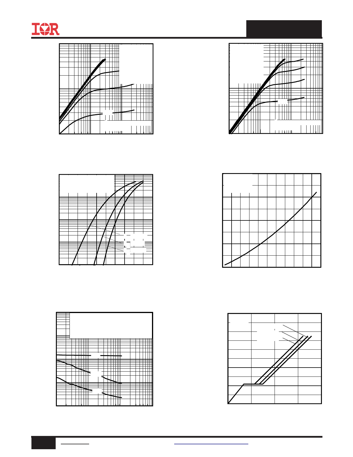
Fig 2. Typical Output Characteristics
Fig 1. Typical Output Characteristics
Fig 3. Typical Transfer Characteristics
Fig 4. Normalized On-Resistance vs. Temperature
Fig 6. Typical Gate Charge vs.Gate-to-Source Voltage
Fig 5. Typical Capacitance vs.Drain-to-Source Voltage
0
10
20
30
40
QG Total Gate Charge (nC)
0
4
8
12
16
20
V
G
S
, G
at
e-
to
-S
ou
rc
e
V
ol
ta
ge
(
V
)
VDS= 120V
VDS= 75V
VDS= 30V
ID= 5.6A
0.1
1
10
100
VDS, Drain-to-Source Voltage (V)
1
10
100
I D
, D
ra
in
-t
o-
S
ou
rc
e
C
ur
re
nt
(
A
)
≤ 60μs PULSE WIDTH
Tj = 25°C
5.5V
VGS
TOP
15V
10V
9.0V
8.0V
7.0V
6.5V
6.0V
BOTTOM
5.5V
0.1
1
10
100
VDS, Drain-to-Source Voltage (V)
1
10
100
I D
, D
ra
in
-t
o-
S
ou
rc
e
C
ur
re
nt
(
A
)
≤ 60μs PULSE WIDTH
Tj = 150°C
5.5V
VGS
TOP
15V
10V
9.0V
8.0V
7.0V
6.5V
6.0V
BOTTOM
5.5V
3.0
4.0
5.0
6.0
7.0
8.0
VGS, Gate-to-Source Voltage (V)
0.01
0.1
1
10
100
I D
, D
ra
in
-t
o-
S
ou
rc
e
C
ur
re
nt
(Α
)
VDS = 25V
≤ 60μs PULSE WIDTH
TJ = 150°C
TJ = 25°C
TJ = -40°C
-60 -40 -20
0
20 40 60 80 100 120 140 160
TJ , Junction Temperature (°C)
0.5
1.0
1.5
2.0
2.5
R
D
S
(o
n)
,
D
ra
in
-t
o-
S
ou
rc
e
O
n
R
es
is
ta
nc
e
(
N
or
m
al
iz
ed
)
ID = 5.6A
VGS = 10V
1
10
100
1000
VDS, Drain-to-Source Voltage (V)
10
100
1000
10000
100000
C
, C
ap
ac
ita
nc
e
(p
F
)
Coss
Crss
Ciss
VGS = 0V, f = 1 MHZ
Ciss = Cgs + Cgd, Cds SHORTED
Crss = Cgd
Coss = Cds + Cgd
IRF6775MTRPbF
4
www.irf.com
©
2014 International Rectifier
Submit Datasheet Feedback
February 26, 2014
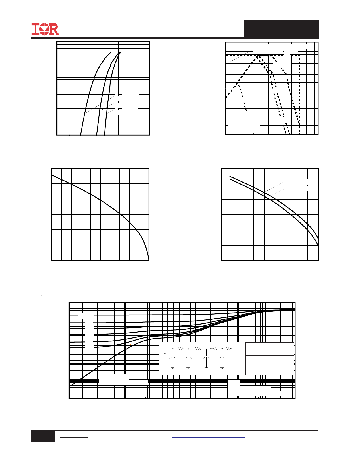
Fig 11. Maximum Effective Transient Thermal Impedance, Junction-to-Ambient
Fig 10. Threshold Voltage vs. Temperature
Fig 9. Maximum Drain Current vs. Case Temperature
Fig 7. Typical Source-Drain Diode Forward Voltage
Fig 8. Maximum Safe Operating Area
0.0
0.5
1.0
1.5
VSD, Source-to-Drain Voltage (V)
0.1
1
10
100
I S
D
, R
ev
er
se
D
ra
in
C
ur
re
nt
(
A
)
VGS = 0V
TJ = 150°C
TJ = 25°C
TJ = -40°C
-75
-50
-25
0
25
50
75
100 125 150
TJ , Temperature ( °C )
2.0
2.5
3.0
3.5
4.0
4.5
5.0
V
G
S
(t
h)
G
at
e
th
re
sh
ol
d
V
ol
ta
ge
(
V
)
ID = 100μA
ID = 250μA
1E-006
1E-005
0.0001
0.001
0.01
0.1
1
10
100
t1 , Rectangular Pulse Duration (sec)
0.001
0.01
0.1
1
10
100
T
he
rm
al
R
es
po
ns
e
(
Z
th
JA
)
0.20
0.10
D = 0.50
0.02
0.01
0.05
SINGLE PULSE
( THERMAL RESPONSE )
Notes:
1. Duty Factor D = t1/t2
2. Peak Tj = P dm x Zthja + Tc
Ri (°C/W)
τi (sec)
1.2801 0.000322
8.7256 0.164798
21.750 2.25760
13.251 69
τ
J
τ
J
τ
1
τ
1
τ
2
τ
2
τ
3
τ
3
R
1
R
1
R
2
R
2
R
3
R
3
Ci=
τi/Ri
Ci=
τi/Ri
τ
A
τ
A
τ
4
τ
4
R
4
R
4
25
50
75
100
125
150
TC , CaseTemperature (°C)
0
5
10
15
20
25
30
I D
,
D
ra
in
C
ur
re
nt
(
A
)
0.1
1
10
100
1000
VDS, Drain-to-Source Voltage (V)
0.1
1
10
100
I D
,
D
ra
in
-t
o-
S
ou
rc
e
C
ur
re
nt
(
A
)
Tc = 25°C
Tj = 150°C
Single Pulse
1msec
10msec
OPERATION IN THIS AREA
LIMITED BY R DS(on)
100μsec
DC
IRF6775MTRPbF
5
www.irf.com
©
2014 International Rectifier
Submit Datasheet Feedback
February 26, 2014
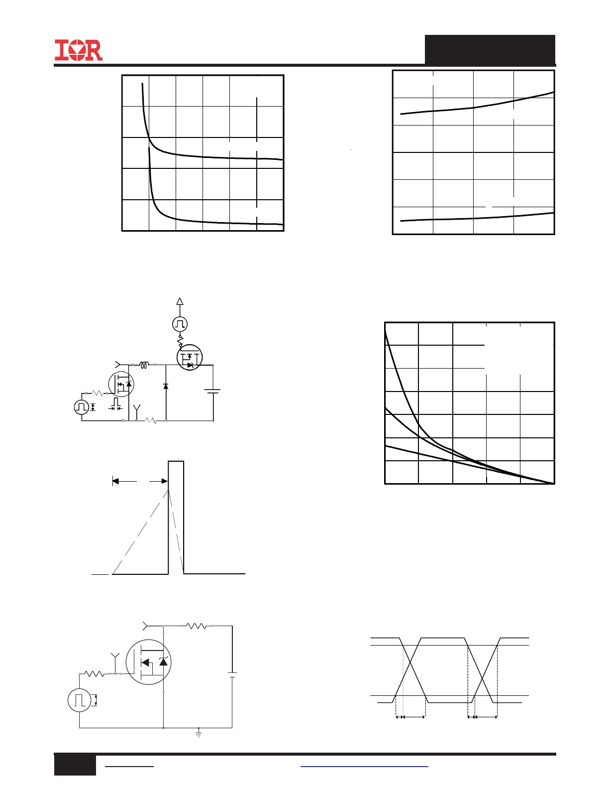
Fig 14. Maximum Avalanche Energy vs. Drain Current
Fig 16a. Switching Time Test Circuit
Fig 16b. Switching Time Waveforms
V
GS
V
DS
90%
10%
t
d(on)
t
d(off)
t
r
t
f
Fig 15b. Unclamped Inductive Waveforms
Fig 15a. Unclamped Inductive Test Circuit
tp
V
(BR)DSS
I
AS
RG
IAS
0.01
Ω
tp
D.U.T
L
VDS
+
- VDD
DRIVER
A
15V
20V
V
GS
Fig 12. On-Resistance vs. Gate Voltage
Fig 13. On-Resistance vs. Drain Current
V
DS
Pulse Width ≤ 1 µs
Duty Factor ≤ 0.1 %
R
D
V
GS
R
G
D.U.T.
10V
+
-V
DD
4
6
8
10
12
14
16
VGS, Gate-to-Source Voltage (V)
40
60
80
100
120
140
R
D
S
(o
n)
,
D
ra
in
-t
o
-S
ou
rc
e
O
n
R
es
is
ta
nc
e
(m
Ω
)
TJ = 25°C
TJ = 125°C
ID = 5.6A
0
5
10
15
20
ID , Drain Current (A)
40
50
60
70
80
90
100
R
D
S
(
on
) ,
D
ra
in
-t
o-
S
ou
rc
e
O
n
R
es
is
ta
nc
e
(m
Ω
)
VGS = 10V
TJ = 125°C
TJ = 25°C
25
50
75
100
125
150
Starting TJ, Junction Temperature (°C)
0
20
40
60
80
100
120
140
E
A
S
,
S
in
gl
e
P
ul
se
A
va
la
nc
he
E
ne
rg
y
(m
J)
I D
TOP
1.1A
1.4A
BOTTOM
11A
IRF6775MTRPbF
6
www.irf.com
©
2014 International Rectifier
Submit Datasheet Feedback
February 26, 2014
Fig 17a. Gate Charge Test Circuit
Fig 17b. Gate Charge Waveform
Vds
Vgs
Id
Vgs(th)
Qgs1
Qgs2
Qgd
Qgodr
1K
VCC
DUT
0
L
S
20K
Fig 18.
Diode Reverse Recovery Test Circuit for HEXFET
®
Power MOSFETs
Circuit Layout Considerations
• Low Stray Inductance
• Ground Plane
• Low Leakage Inductance
Current Transformer
P.W.
Period
di/dt
Diode Recovery
dv/dt
Ripple
≤ 5%
Body Diode Forward Drop
Re-Applied
Voltage
Reverse
Recovery
Current
Body Diode Forward
Current
V
GS
=10V
V
DD
I
SD
Driver Gate Drive
D.U.T. I
SD
Waveform
D.U.T. V
DS
Waveform
Inductor Curent
D =
P.W.
Period
***
V
GS
= 5V for Logic Level Devices
***
+
-
+
+
+
-
-
-
R
G
V
DD
• dv/dt controlled by R
G
• Driver same type as D.U.T.
• I
SD
controlled by Duty Factor "D"
• D.U.T. - Device Under Test
D.U.T
**
*
*
Use P-Channel Driver for P-Channel Measurements
**
Reverse Polarity for P-Channel
IRF6775MTRPbF
7
www.irf.com
©
2014 International Rectifier
Submit Datasheet Feedback
February 26, 2014
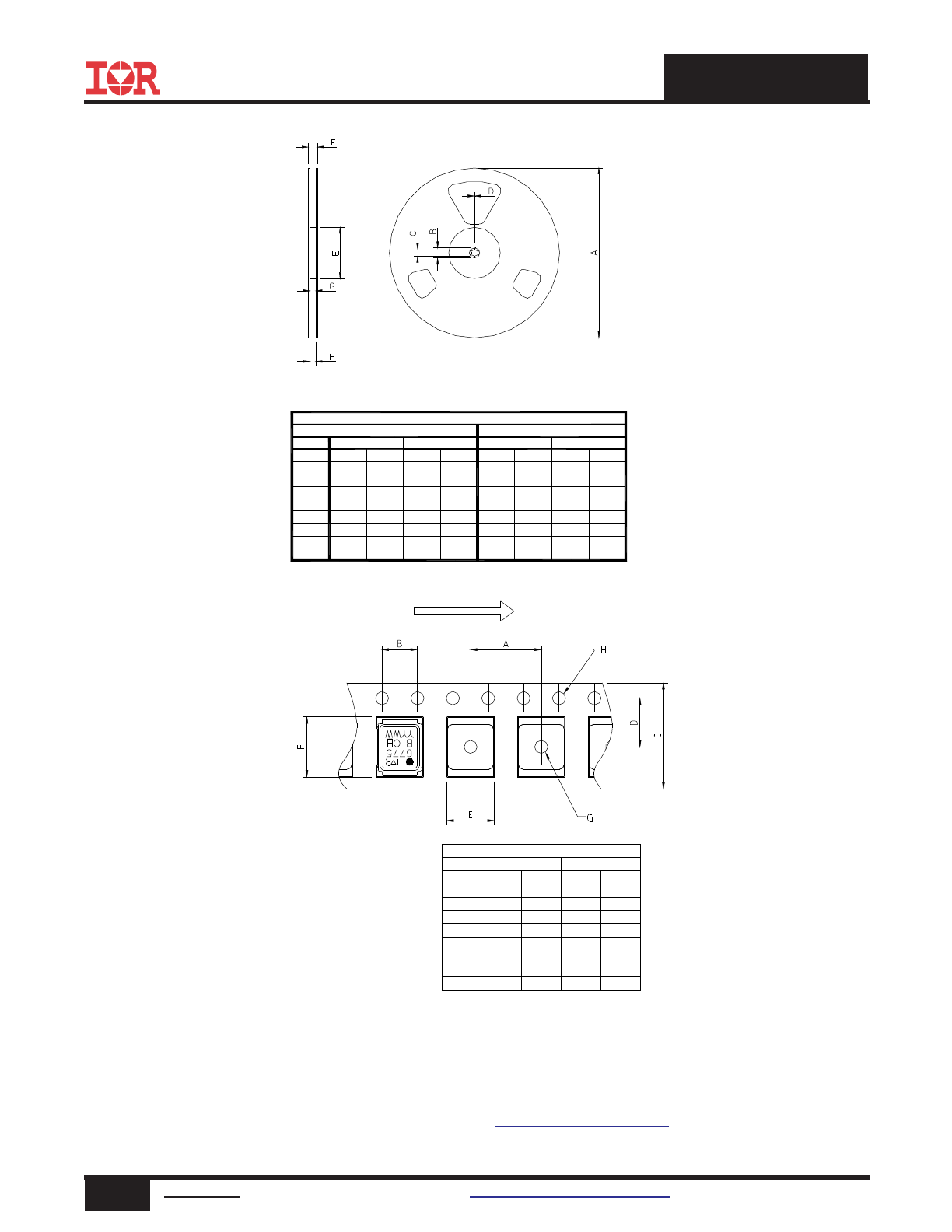
DirectFET™
Substrate and PCB Layout, MZ Outline
(
Medium Size Can, Z-Designation).
Please see DirectFET application note AN-1035 for all details regarding PCB assembly using DirectFET. This
includes all recommendations for stencil and substrate designs.
Note: For the most current drawing please refer to IR website at:
http://www.irf.com/package/
IRF6775MTRPbF
8
www.irf.com
©
2014 International Rectifier
Submit Datasheet Feedback
February 26, 2014
DirectFET
Outline Dimension, MZ Outline
(Medium Size Can, Z-Designation).
Please see DirectFET application note AN-1035 for all details regarding PCB assembly using DirectFET. This
includes all recommendations for stencil and substrate designs.
DirectFET
Part Marking
MAX
0.250
0.201
0.156
0.018
0.028
0.028
0.038
0.026
0.013
0.050
0.105
0.0274
0.0031
0.007
MAX
0.246
0.189
0.152
0.014
0.027
0.027
0.037
0.025
0.011
0.044
0.100
0.0235
0.0008
0.003
IMPERIAL
CODE
A
B
C
D
E
F
G
H
J
K
L
M
R
P
MAX
6.35
5.05
3.95
0.45
0.72
0.72
0.97
0.67
0.32
1.26
2.66
0.676
0.080
0.17
MIN
6.25
4.80
3.85
0.35
0.68
0.68
0.93
0.63
0.28
1.13
2.53
0.616
0.020
0.08
METRIC
DIMENSIONS
LOGO
GATE MARKING
BATCH NUMBER
PART NUMBER
DATE CODE
Line above the last character of
the date code indicates "Lead-Free"
Note: For the most current drawing please refer to IR website at:
http://www.irf.com/package/
IRF6775MTRPbF
9
www.irf.com
©
2014 International Rectifier
Submit Datasheet Feedback
February 26, 2014
DirectFET
Tape & Reel Dimension (Showing component orientation).
LOADED TAPE FEED DIRECTION
MIN
7.90
3.90
11.90
5.45
5.10
6.50
1.50
1.50
NOTE: CONTROLLING
DIMENSIONS IN MM
CODE
A
B
C
D
E
F
G
H
MAX
8.10
4.10
12.30
5.55
5.30
6.70
N.C
1.60
MIN
0.311
0.154
0.469
0.215
0.201
0.256
0.059
0.059
MAX
0.319
0.161
0.484
0.219
0.209
0.264
N.C
0.063
DIMENSIONS
METRIC
IMPERIAL
REEL DIMENSIONS
NOTE: Controlling dimensions in mm
Std reel quantity is 4800 parts. (ordered as IRF6775TRPBF). For 1000 parts on 7"
reel, order IRF6775TR1PBF
STANDARD OPTION (QTY 4800)
MIN
330.0
20.2
12.8
1.5
100.0
N.C
12.4
11.9
CODE
A
B
C
D
E
F
G
H
MAX
N.C
N.C
13.2
N.C
N.C
18.4
14.4
15.4
MIN
12.992
0.795
0.504
0.059
3.937
N.C
0.488
0.469
MAX
N.C
N.C
0.520
N.C
N.C
0.724
0.567
0.606
METRIC
IMPERIAL
TR1 OPTION (QTY 1000)
IMPERIAL
MIN
6.9
0.75
0.53
0.059
2.31
N.C
0.47
0.47
MAX
N.C
N.C
12.8
N.C
N.C
13.50
12.01
12.01
MIN
177.77
19.06
13.5
1.5
58.72
N.C
11.9
11.9
METRIC
MAX
N.C
N.C
0.50
N.C
N.C
0.53
N.C
N.C
Note: For the most current drawing please refer to IR website at:
http://www.irf.com/package/
IRF6775MTRPbF
10
www.irf.com
©
2014 International Rectifier
Submit Datasheet Feedback
February 26, 2014
Data and specifications subject to change without notice.
This product has been designed and qualified for the Consumer market.
Qualification Standards can be found on IR’s Web site.
IR WORLD HEADQUARTERS: 101 N. Sepulveda Blvd., El Segundo, California 90245, USA
To contact International Rectifier, please visit
http://www.irf.com/whoto-call/
Date
Comments
• Updated SOA curve figure 8 to extend x axis to 150V because this device is 150V, on page 4.
• Updated datasheet with new IR corporate template.
Revision History
2/26/2014
Notes
through
are on page 2
Applicable DirectFET Outline and Substrate Outline (see p. 6, 7 for details)
Description
This Digital Audio MOSFET is specifically designed for Class-D audio amplifier applications. This MOSFET utilizes the
latest processing techniques to achieve low on-resistance per silicon area. Furthermore, gate charge, body-diode reverse
recovery and internal gate resistance are optimized to improve key Class-D audio amplifier performance factors such as
efficiency, THD, and EMI.
The IRF6775MPbF device utilizes DirectFET
TM
packaging technology. DirectFET
TM
packaging technology offers lower parasitic
inductance and resistance when compared to conventional wirebonded SOIC packaging. Lower inductance improves EMI
performance by reducing the voltage ringing that accompanies fast current transients. The DirectFET
TM
package is compatible
with existing layout geometries used in power applications, PCB assembly equipment and vapor phase, infra-red or convection
soldering techniques, when application note AN-1035 is followed regarding the manufacturing method and processes. The
DirectFET
TM
package also allows dual sided cooling to maximize thermal transfer in power systems, improving thermal resis-
tance and power dissipation. These features combine to make this MOSFET a highly efficient, robust and reliable device for
Class-D audio amplifier applications.
Features
• Latest MOSFET Silicon technology
• Key parameters optimized for Class-D audio amplifier
applications
• Low R
DS(on)
for improved efficiency
• Low Q
g
for better THD and improved efficiency
• Low Q
rr
for better THD and lower EMI
• Low package stray inductance for reduced ringing and lower EMI
• Can deliver up to 250W per channel into 4Ω Load in
Half-Bridge Configuration Amplifier
• Dual sided cooling compatible
· Compatible with existing surface mount technologies
· RoHS compliant containing no lead or bromide
·Lead-Free (Qualified up to 260°C Reflow)
DirectFET
ISOMETRIC
MZ
SQ
SX
ST
SH
MQ
MX
MT
MN
MZ
&
)
5
5
&
V
DS
150
V
R
DS(on)
typ. @ V
GS
= 10V
47
m
:
Q
g
typ.
25.0
nC
R
G(int)
max.
3.0
Key Parameters
Absolute Maximum Ratings
Parameter
Units
V
DS
Drain-to-Source Voltage
V
V
GS
Gate-to-Source Voltage
I
D
@ T
C
= 25°C
Continuous Drain Current, V
GS
@ 10V
I
D
@ T
A
= 25°C
Continuous Drain Current, V
GS
@ 10V
A
I
D
@ T
A
= 70°C
Continuous Drain Current, V
GS
@ 10V
I
DM
Pulsed Drain Current
c
P
D
@T
C
= 25°C
Maximum Power Dissipation
W
P
D
@T
A
= 25°C
Power Dissipation
e
P
D
@T
A
= 70°C
Power Dissipation
e
E
AS
Single Pulse Avalanche Energy
d
mJ
I
AR
Avalanche Current
c
A
Linear Derating Factor
e
W/°C
T
J
Operating Junction and
°C
T
STG
Storage Temperature Range
Thermal Resistance
Parameter
Typ.
Max.
Units
R
θJA
Junction-to-Ambient
ek
–––
45
°C/W
R
θJA
Junction-to-Ambient
hk
12.5
–––
R
θJA
Junction-to-Ambient
ik
20
–––
R
θJC
Junction-to-Case
jk
–––
1.4
R
θJ-PCB
Junction-to-PCB Mounted
1.4
–––
89
Max.
4.9
3.9
39
150
± 20
28
-40 to + 150
0.022
2.8
1.8
33
5.6
IRF6775MTRPbF
DIGITAL AUDIO MOSFET
1
www.irf.com
©
2014 International Rectifier
Submit Datasheet Feedback
February 26, 2014
IRF6775MTRPbF
2
www.irf.com
©
2014 International Rectifier
Submit Datasheet Feedback
February 26, 2014
S
D
G
Notes:
Repetitive rating; pulse width limited by
max. junction temperature.
Starting T
J
= 25°C, L = 0.53mH, R
G
= 25
Ω, I
AS
= 11.2A.
Surface mounted on 1 in. square Cu board.
Pulse width ≤ 400μs; duty cycle ≤ 2%.
C
oss
eff. is a fixed capacitance that gives the same
charging time as C
oss
while V
DS
is rising from 0 to 80% V
DSS
.
Used double sided cooling , mounting pad with large heatsink.
Mounted on minimum footprint full size board with
metalized back and with small clip heatsink.
T
C
measured with thermal couple mounted to top
(Drain) of part.
R
θ
is measured at T
J
of approximately 90°C.
Static @ T
J
= 25°C (unless otherwise specified)
Parameter
Min.
Typ.
Max.
Units
V
(BR)DSS
Drain-to-Source Breakdown Voltage
150
–––
–––
V
ΔV
(BR)DSS
/
ΔT
J
Breakdown Voltage Temp. Coefficient
–––
0.17
–––
V/°C
R
DS(on)
Static Drain-to-Source On-Resistance
–––
47
56
m
Ω
V
GS(th)
Gate Threshold Voltage
3.0
–––
5.0
V
I
DSS
Drain-to-Source Leakage Current
–––
–––
20
μA
–––
–––
250
I
GSS
Gate-to-Source Forward Leakage
–––
–––
100
nA
Gate-to-Source Reverse Leakage
–––
–––
-100
R
G(int)
Internal Gate Resistance
–––
–––
3.0
Ω
Dynamic @ T
J
= 25°C (unless otherwise specified)
Parameter
Min.
Typ.
Max.
Units
gfs
Forward Transconductance
11
–––
–––
S
Q
g
Total Gate Charge
–––
25
36
V
DS
= 75V
Q
gs1
Pre-Vth Gate-to-Source Charge
–––
5.8
–––
V
GS
= 10V
Q
gs2
Post-Vth Gate-to-Source Charge
–––
1.4
–––
I
D
= 5.6A
Q
gd
Gate-to-Drain Charge
–––
6.6
–––
nC
See Fig. 6 and 17
Q
godr
Gate Charge Overdrive
–––
11
–––
Q
sw
Switch Charge (Q
gs2
+ Q
gd
)
–––
8.0
–––
t
d(on)
Turn-On Delay Time
–––
5.9
–––
t
r
Rise Time
–––
7.8
–––
t
d(off)
Turn-Off Delay Time
–––
5.8
–––
ns
t
f
Fall Time
–––
15
–––
C
iss
Input Capacitance
–––
1411
–––
C
oss
Output Capacitance
–––
193
–––
C
rss
Reverse Transfer Capacitance
–––
40
–––
pF
C
oss
Output Capacitance
–––
1557
–––
C
oss
Output Capacitance
–––
93
–––
C
oss
eff.
Effective Output Capacitance
–––
175
–––
Diode Characteristics
Parameter
Min.
Typ.
Max.
Units
I
S
Continuous Source Current
–––
–––
28
(Body Diode)
A
I
SM
Pulsed Source Current
–––
–––
39
(Body Diode)
c
V
SD
Diode Forward Voltage
–––
–––
1.3
V
t
rr
Reverse Recovery Time
–––
62
–––
ns
Q
rr
Reverse Recovery Charge
–––
164
–––
nC
V
DD
= 75V
I
D
= 5.6A
R
G
= 6.0
Ω
V
GS
= 20V
V
GS
= -20V
Conditions
V
DS
= 50V, I
D
= 5.6A
T
J
= 25°C, I
S
= 5.6A, V
GS
= 0V
f
T
J
= 25°C, I
F
= 5.6A, V
DD
= 25V
di/dt = 100A/μs
f
Conditions
V
GS
= 0V, I
D
= 250μA
Reference to 25°C, I
D
= 1mA
V
GS
= 10V, I
D
= 5.6A
f
V
DS
= V
GS
, I
D
= 100μA
V
DS
= 150V, V
GS
= 0V
V
DS
= 120V, V
GS
= 0V, T
J
= 125°C
MOSFET symbol
showing the
integral reverse
p-n junction diode.
Conditions
V
GS
= 10V
f
V
GS
= 0V
V
DS
= 25V
ƒ = 1.0MHz
V
GS
= 0V, V
DS
= 0V to 120V
g
V
GS
= 0V, V
DS
= 1.0V, ƒ = 1.0MHz
V
GS
= 0V, V
DS
= 120V, ƒ = 1.0MHz
IRF6775MTRPbF
3
www.irf.com
©
2014 International Rectifier
Submit Datasheet Feedback
February 26, 2014
Fig 2. Typical Output Characteristics
Fig 1. Typical Output Characteristics
Fig 3. Typical Transfer Characteristics
Fig 4. Normalized On-Resistance vs. Temperature
Fig 6. Typical Gate Charge vs.Gate-to-Source Voltage
Fig 5. Typical Capacitance vs.Drain-to-Source Voltage
0
10
20
30
40
QG Total Gate Charge (nC)
0
4
8
12
16
20
V
G
S
, G
at
e-
to
-S
ou
rc
e
V
ol
ta
ge
(
V
)
VDS= 120V
VDS= 75V
VDS= 30V
ID= 5.6A
0.1
1
10
100
VDS, Drain-to-Source Voltage (V)
1
10
100
I D
, D
ra
in
-t
o-
S
ou
rc
e
C
ur
re
nt
(
A
)
≤ 60μs PULSE WIDTH
Tj = 25°C
5.5V
VGS
TOP
15V
10V
9.0V
8.0V
7.0V
6.5V
6.0V
BOTTOM
5.5V
0.1
1
10
100
VDS, Drain-to-Source Voltage (V)
1
10
100
I D
, D
ra
in
-t
o-
S
ou
rc
e
C
ur
re
nt
(
A
)
≤ 60μs PULSE WIDTH
Tj = 150°C
5.5V
VGS
TOP
15V
10V
9.0V
8.0V
7.0V
6.5V
6.0V
BOTTOM
5.5V
3.0
4.0
5.0
6.0
7.0
8.0
VGS, Gate-to-Source Voltage (V)
0.01
0.1
1
10
100
I D
, D
ra
in
-t
o-
S
ou
rc
e
C
ur
re
nt
(Α
)
VDS = 25V
≤ 60μs PULSE WIDTH
TJ = 150°C
TJ = 25°C
TJ = -40°C
-60 -40 -20
0
20 40 60 80 100 120 140 160
TJ , Junction Temperature (°C)
0.5
1.0
1.5
2.0
2.5
R
D
S
(o
n)
,
D
ra
in
-t
o-
S
ou
rc
e
O
n
R
es
is
ta
nc
e
(
N
or
m
al
iz
ed
)
ID = 5.6A
VGS = 10V
1
10
100
1000
VDS, Drain-to-Source Voltage (V)
10
100
1000
10000
100000
C
, C
ap
ac
ita
nc
e
(p
F
)
Coss
Crss
Ciss
VGS = 0V, f = 1 MHZ
Ciss = Cgs + Cgd, Cds SHORTED
Crss = Cgd
Coss = Cds + Cgd
IRF6775MTRPbF
4
www.irf.com
©
2014 International Rectifier
Submit Datasheet Feedback
February 26, 2014
Fig 11. Maximum Effective Transient Thermal Impedance, Junction-to-Ambient
Fig 10. Threshold Voltage vs. Temperature
Fig 9. Maximum Drain Current vs. Case Temperature
Fig 7. Typical Source-Drain Diode Forward Voltage
Fig 8. Maximum Safe Operating Area
0.0
0.5
1.0
1.5
VSD, Source-to-Drain Voltage (V)
0.1
1
10
100
I S
D
, R
ev
er
se
D
ra
in
C
ur
re
nt
(
A
)
VGS = 0V
TJ = 150°C
TJ = 25°C
TJ = -40°C
-75
-50
-25
0
25
50
75
100 125 150
TJ , Temperature ( °C )
2.0
2.5
3.0
3.5
4.0
4.5
5.0
V
G
S
(t
h)
G
at
e
th
re
sh
ol
d
V
ol
ta
ge
(
V
)
ID = 100μA
ID = 250μA
1E-006
1E-005
0.0001
0.001
0.01
0.1
1
10
100
t1 , Rectangular Pulse Duration (sec)
0.001
0.01
0.1
1
10
100
T
he
rm
al
R
es
po
ns
e
(
Z
th
JA
)
0.20
0.10
D = 0.50
0.02
0.01
0.05
SINGLE PULSE
( THERMAL RESPONSE )
Notes:
1. Duty Factor D = t1/t2
2. Peak Tj = P dm x Zthja + Tc
Ri (°C/W)
τi (sec)
1.2801 0.000322
8.7256 0.164798
21.750 2.25760
13.251 69
τ
J
τ
J
τ
1
τ
1
τ
2
τ
2
τ
3
τ
3
R
1
R
1
R
2
R
2
R
3
R
3
Ci=
τi/Ri
Ci=
τi/Ri
τ
A
τ
A
τ
4
τ
4
R
4
R
4
25
50
75
100
125
150
TC , CaseTemperature (°C)
0
5
10
15
20
25
30
I D
,
D
ra
in
C
ur
re
nt
(
A
)
0.1
1
10
100
1000
VDS, Drain-to-Source Voltage (V)
0.1
1
10
100
I D
,
D
ra
in
-t
o-
S
ou
rc
e
C
ur
re
nt
(
A
)
Tc = 25°C
Tj = 150°C
Single Pulse
1msec
10msec
OPERATION IN THIS AREA
LIMITED BY R DS(on)
100μsec
DC
IRF6775MTRPbF
5
www.irf.com
©
2014 International Rectifier
Submit Datasheet Feedback
February 26, 2014
Fig 14. Maximum Avalanche Energy vs. Drain Current
Fig 16a. Switching Time Test Circuit
Fig 16b. Switching Time Waveforms
V
GS
V
DS
90%
10%
t
d(on)
t
d(off)
t
r
t
f
Fig 15b. Unclamped Inductive Waveforms
Fig 15a. Unclamped Inductive Test Circuit
tp
V
(BR)DSS
I
AS
RG
IAS
0.01
Ω
tp
D.U.T
L
VDS
+
- VDD
DRIVER
A
15V
20V
V
GS
Fig 12. On-Resistance vs. Gate Voltage
Fig 13. On-Resistance vs. Drain Current
V
DS
Pulse Width ≤ 1 µs
Duty Factor ≤ 0.1 %
R
D
V
GS
R
G
D.U.T.
10V
+
-V
DD
4
6
8
10
12
14
16
VGS, Gate-to-Source Voltage (V)
40
60
80
100
120
140
R
D
S
(o
n)
,
D
ra
in
-t
o
-S
ou
rc
e
O
n
R
es
is
ta
nc
e
(m
Ω
)
TJ = 25°C
TJ = 125°C
ID = 5.6A
0
5
10
15
20
ID , Drain Current (A)
40
50
60
70
80
90
100
R
D
S
(
on
) ,
D
ra
in
-t
o-
S
ou
rc
e
O
n
R
es
is
ta
nc
e
(m
Ω
)
VGS = 10V
TJ = 125°C
TJ = 25°C
25
50
75
100
125
150
Starting TJ, Junction Temperature (°C)
0
20
40
60
80
100
120
140
E
A
S
,
S
in
gl
e
P
ul
se
A
va
la
nc
he
E
ne
rg
y
(m
J)
I D
TOP
1.1A
1.4A
BOTTOM
11A
IRF6775MTRPbF
6
www.irf.com
©
2014 International Rectifier
Submit Datasheet Feedback
February 26, 2014
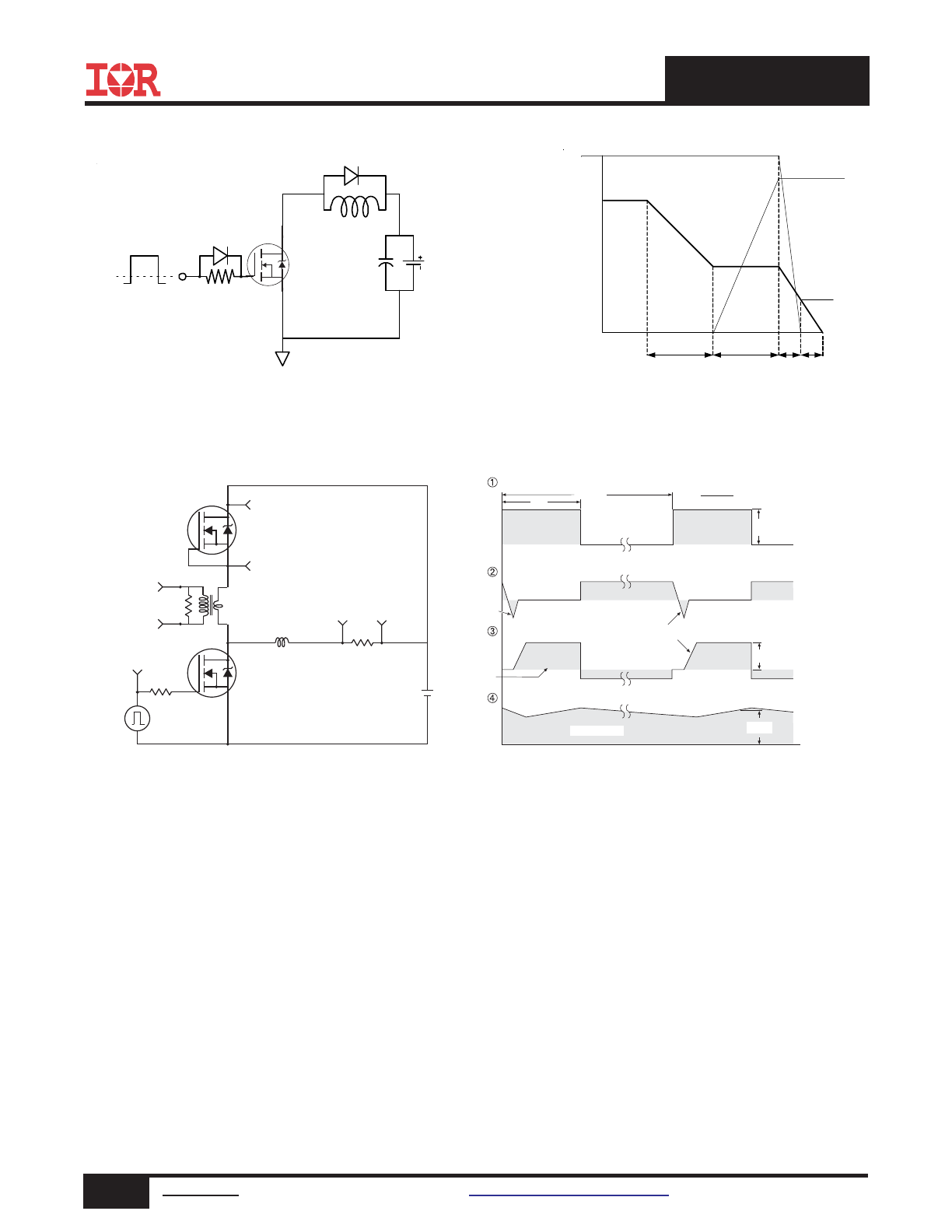
Fig 17a. Gate Charge Test Circuit
Fig 17b. Gate Charge Waveform
Vds
Vgs
Id
Vgs(th)
Qgs1
Qgs2
Qgd
Qgodr
1K
VCC
DUT
0
L
S
20K
Fig 18.
Diode Reverse Recovery Test Circuit for HEXFET
®
Power MOSFETs
Circuit Layout Considerations
• Low Stray Inductance
• Ground Plane
• Low Leakage Inductance
Current Transformer
P.W.
Period
di/dt
Diode Recovery
dv/dt
Ripple
≤ 5%
Body Diode Forward Drop
Re-Applied
Voltage
Reverse
Recovery
Current
Body Diode Forward
Current
V
GS
=10V
V
DD
I
SD
Driver Gate Drive
D.U.T. I
SD
Waveform
D.U.T. V
DS
Waveform
Inductor Curent
D =
P.W.
Period
***
V
GS
= 5V for Logic Level Devices
***
+
-
+
+
+
-
-
-
R
G
V
DD
• dv/dt controlled by R
G
• Driver same type as D.U.T.
• I
SD
controlled by Duty Factor "D"
• D.U.T. - Device Under Test
D.U.T
**
*
*
Use P-Channel Driver for P-Channel Measurements
**
Reverse Polarity for P-Channel
IRF6775MTRPbF
7
www.irf.com
©
2014 International Rectifier
Submit Datasheet Feedback
February 26, 2014
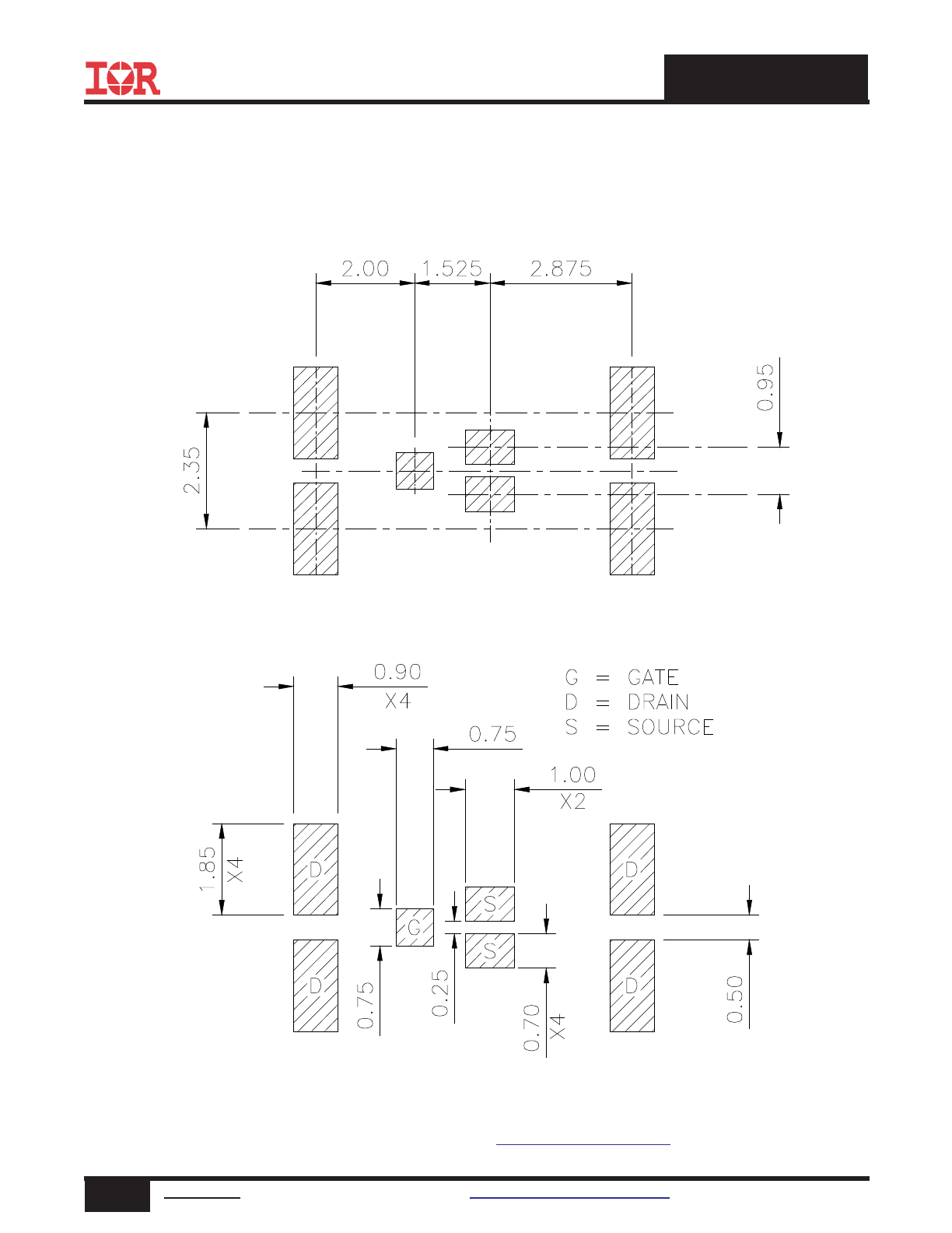
DirectFET™
Substrate and PCB Layout, MZ Outline
(
Medium Size Can, Z-Designation).
Please see DirectFET application note AN-1035 for all details regarding PCB assembly using DirectFET. This
includes all recommendations for stencil and substrate designs.
Note: For the most current drawing please refer to IR website at:
http://www.irf.com/package/
IRF6775MTRPbF
8
www.irf.com
©
2014 International Rectifier
Submit Datasheet Feedback
February 26, 2014
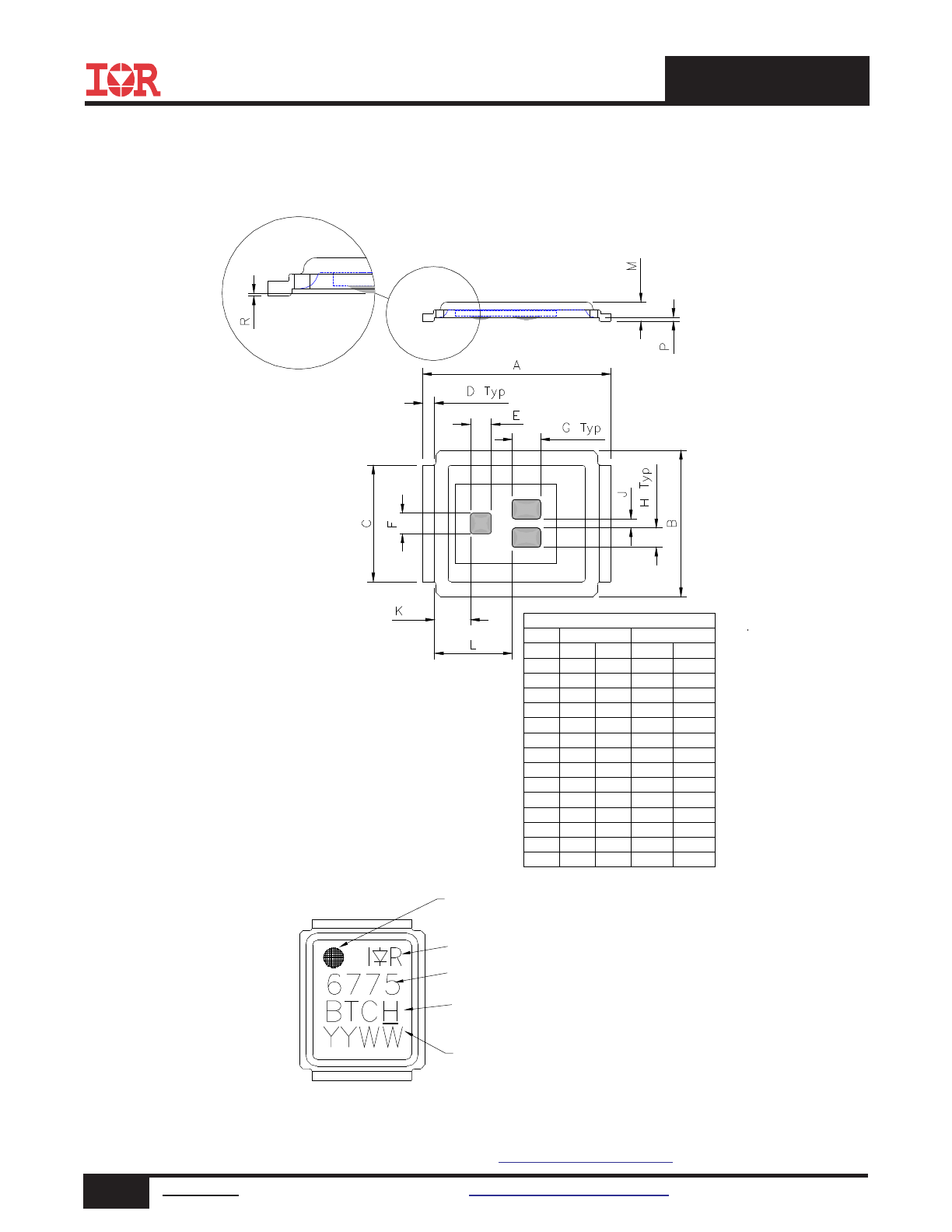
DirectFET
Outline Dimension, MZ Outline
(Medium Size Can, Z-Designation).
Please see DirectFET application note AN-1035 for all details regarding PCB assembly using DirectFET. This
includes all recommendations for stencil and substrate designs.
DirectFET
Part Marking
MAX
0.250
0.201
0.156
0.018
0.028
0.028
0.038
0.026
0.013
0.050
0.105
0.0274
0.0031
0.007
MAX
0.246
0.189
0.152
0.014
0.027
0.027
0.037
0.025
0.011
0.044
0.100
0.0235
0.0008
0.003
IMPERIAL
CODE
A
B
C
D
E
F
G
H
J
K
L
M
R
P
MAX
6.35
5.05
3.95
0.45
0.72
0.72
0.97
0.67
0.32
1.26
2.66
0.676
0.080
0.17
MIN
6.25
4.80
3.85
0.35
0.68
0.68
0.93
0.63
0.28
1.13
2.53
0.616
0.020
0.08
METRIC
DIMENSIONS
LOGO
GATE MARKING
BATCH NUMBER
PART NUMBER
DATE CODE
Line above the last character of
the date code indicates "Lead-Free"
Note: For the most current drawing please refer to IR website at:
http://www.irf.com/package/
IRF6775MTRPbF
9
www.irf.com
©
2014 International Rectifier
Submit Datasheet Feedback
February 26, 2014
DirectFET
Tape & Reel Dimension (Showing component orientation).
LOADED TAPE FEED DIRECTION
MIN
7.90
3.90
11.90
5.45
5.10
6.50
1.50
1.50
NOTE: CONTROLLING
DIMENSIONS IN MM
CODE
A
B
C
D
E
F
G
H
MAX
8.10
4.10
12.30
5.55
5.30
6.70
N.C
1.60
MIN
0.311
0.154
0.469
0.215
0.201
0.256
0.059
0.059
MAX
0.319
0.161
0.484
0.219
0.209
0.264
N.C
0.063
DIMENSIONS
METRIC
IMPERIAL
REEL DIMENSIONS
NOTE: Controlling dimensions in mm
Std reel quantity is 4800 parts. (ordered as IRF6775TRPBF). For 1000 parts on 7"
reel, order IRF6775TR1PBF
STANDARD OPTION (QTY 4800)
MIN
330.0
20.2
12.8
1.5
100.0
N.C
12.4
11.9
CODE
A
B
C
D
E
F
G
H
MAX
N.C
N.C
13.2
N.C
N.C
18.4
14.4
15.4
MIN
12.992
0.795
0.504
0.059
3.937
N.C
0.488
0.469
MAX
N.C
N.C
0.520
N.C
N.C
0.724
0.567
0.606
METRIC
IMPERIAL
TR1 OPTION (QTY 1000)
IMPERIAL
MIN
6.9
0.75
0.53
0.059
2.31
N.C
0.47
0.47
MAX
N.C
N.C
12.8
N.C
N.C
13.50
12.01
12.01
MIN
177.77
19.06
13.5
1.5
58.72
N.C
11.9
11.9
METRIC
MAX
N.C
N.C
0.50
N.C
N.C
0.53
N.C
N.C
Note: For the most current drawing please refer to IR website at:
http://www.irf.com/package/
IRF6775MTRPbF
10
www.irf.com
©
2014 International Rectifier
Submit Datasheet Feedback
February 26, 2014
Data and specifications subject to change without notice.
This product has been designed and qualified for the Consumer market.
Qualification Standards can be found on IR’s Web site.
IR WORLD HEADQUARTERS: 101 N. Sepulveda Blvd., El Segundo, California 90245, USA
To contact International Rectifier, please visit
http://www.irf.com/whoto-call/
Date
Comments
• Updated SOA curve figure 8 to extend x axis to 150V because this device is 150V, on page 4.
• Updated datasheet with new IR corporate template.
Revision History
2/26/2014