
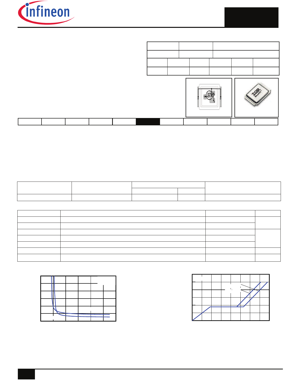
Base part number
Standard Pack
Orderable Part Number
Form
Quantity
IRF6648TRPbF
DirectFET
™
Medium Can
Tape and Reel
4800
IRF6648TRPbF
Package Type
Fig 1. Typical On-Resistance vs. Gate Voltage
DirectFET™ ISOMETRIC
MN
V
DSS
V
GS
R
DS(on)
60V min
±20V max
5.5m
@ 10V
Applicable DirectFET Outline and Substrate Outline (see p.7,8 for details)
SH
SJ
SP MZ
MN
Description
The IRF6648PbF combines the latest HEXFET® Power MOSFET Silicon technology with the advanced DirectFET™ packaging to achieve
the lowest on-state resistance in a package that has the footprint of a SO-8 and only 0.7 mm profile. The DirectFET™ package is compati-
ble with existing layout geometries used in power applications, PCB assembly equipment and vapor phase, infra-red or convection soldering
techniques. Application note AN-1035 is followed regarding the manufacturing methods and processes. The DirectFET™ package allows
dual sided cooling to maximize thermal transfer in power systems, improving previous best thermal resistance by 80%.
The IRF6648PbF is an optimized switch for use in synchronous rectification circuits with 5-12Vout, and is also ideal for use as a primary
side switch in 24Vin forward converters. The reduced total losses in the device coupled with the high level of thermal performance enables
high efficiency and low temperatures, which are key for system reliability improvements, and makes this device ideal for high performance.
Absolute Maximum Ratings
Parameter Max.
Units
V
DS
Drain-to-Source Voltage
60
V
V
GS
Gate-to-Source Voltage
±20
I
D
@ T
C
= 25°C
Continuous Drain Current, V
GS
@ 10V (Silicon Limited) 86
A
I
D
@ T
C
= 70°C
Continuous Drain Current, V
GS
@ 10V (Silicon Limited) 69
I
DM
Pulsed Drain Current 260
E
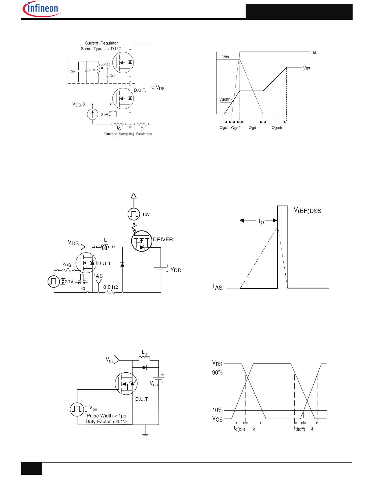
AS
Single Pulse Avalanche Energy 47
mJ
I
AR
Avalanche Current 34
A
Notes
Click on this section to link to the appropriate technical paper.
Click on this section to link to the DirectFET Website.
Surface mounted on 1 in. square Cu board, steady state.
TC measured with thermocouple mounted to top (Drain) of part.
Repetitive rating; pulse width limited by max. junction temperature.
Starting T
J
= 25°C, L = 0.082mH, R
G
= 25
, I
AS
= 34A.
Fig 2. Typical Total Gate Charge vs. Gate-to-Source Voltage
IRF6648PbF
IRF6648TRPbF
Typical values (unless otherwise specified)
Q
g tot
Q
gd
Q
gs2
Q
rr
Q
oss
V
gs(th)
36nC 14nC 2.7nC 37nC 11nC 4.0V
RoHs Compliant
Lead-Free (Qualified up to 260°C Reflow)
Application Specific MOSFETs
Optimized for Synchronous Rectification for
5V to 12V outputs
Low Conduction Losses
Ideal for 24V input Primary Side Forward Converters
Low Profile (<0.7mm)
Dual Sided Cooling Compatible
Compatible with existing Surface Mount Techniques
DirectFET™ Power MOSFET
1
2017-04-06
4
6
8
10
12
14
16
VGS, Gate -to -Source Voltage (V)
0
10
20
30
40
50
60
T
yp
ic
a
l R
D
S
(o
n)
(
m
)
ID = 17A
TJ = 25°C
TJ = 125°C
0
5
10
15
20
25
30
35
40
QG, Total Gate Charge (nC)
0.0
2.0
4.0
6.0
8.0
10.0
12.0
V
G
S
, G
at
e-
to
-S
ou
rc
e
V
ol
ta
ge
(
V
)
VDS= 48V
VDS= 30V
ID= 17A
IRF6648TRPbF
2
2017-04-06
Static @ T
J
= 25°C (unless otherwise specified)
Parameter Min.
Typ.
Max.
Units
Conditions
BV
DSS
Drain-to-Source Breakdown Voltage
60
––– –––
V
V
GS
= 0V, I
D
= 250µA
V
DSS
/
T
J
Breakdown Voltage Temp. Coefficient
––– 0.076 –––
V/°C Reference to 25°c, I
D
= 1mA
R
DS(on)
Static Drain-to-Source On-Resistance
–––
5.5
7.0
m
V
GS
= 10V, I
D
= 17A
V
GS(th)
Gate Threshold Voltage
3.0
4.0
4.9
V
V
DS
= V
GS
, I
D
= 150µA
V
GS(th)
/
T
J
Gate Threshold Voltage Temp. Coefficient
–––
-11 ––– mV/°C
I
DSS
Drain-to-Source Leakage Current
––– ––– 20
V
DS
= 60 V, V
GS
= 0V
––– ––– 250
V
DS
= 48 V, V
GS
= 0V, T
J
= 125°C
I
GSS
Gate-to-Source Forward Leakage
–––
––– 100
nA
V
GS
= 20V
Gate-to-Source Reverse Leakage
–––
––– -100
V
GS
= -20V
gfs Forward
Transconductance
31
–––
–––
S
V
DS
= 10V, I
D
= 17A
Q
g
Total Gate Charge
–––
36
50
nC
Q
gs1
Pre– Vth Gate-to-Source Charge
–––
7.5
–––
V
DS
= 30V
Q
gs2
Post– Vth Gate-to-Source Charge
–––
2.7
–––
V
GS
= 10V
Q
gd
Gate-to-Drain Charge
–––
14
21
I
D
= 17A
Q
godr
Gate Charge Overdrive
–––
12
–––
See Fig 15
Q
sw
Switch Charge (Q
gs2 +
Q
gd)
––– 17 –––
Q
oss
Output Charge
–––
21
–––
nC
V
DS
= 16V, V
GS
= 0V
R
G(Internal)
Gate Resistance
–––
1.0
–––
t
d(on)
Turn-On Delay Time
–––
16
–––
ns
V
DD
= 30V, V
GS
= 10V
t
r
Rise Time
–––
29
–––
I
D
= 17A
t
d(off)
Turn-Off Delay Time
–––
28
–––
R
G
= 6.2
t
f
Fall Time
–––
13
–––
See Fig 16 & 17
C
iss
Input Capacitance
––– 2120 –––
pF
V
GS
= 0V
C
oss
Output Capacitance
–––
600 –––
V
DS
= 25V
C
rss
Reverse Transfer Capacitance
–––
170 –––
ƒ = 1.0MHz
Diode Characteristics
Parameter
Min. Typ. Max. Units
Conditions
I
S
Continuous Source Current
––– ––– 81
A
MOSFET symbol
(Body Diode)
showing the
I
SM
Pulsed Source Current
––– ––– 260
integral reverse
(Body Diode)
p-n junction diode.
V
SD
Diode Forward Voltage
–––
–––
1.3
V
T
J
= 25°C, I
S
= 17A, V
GS
= 0V
t
rr
Reverse Recovery Time
–––
31
47
ns T
J
= 25°C, I
F
= 17A,V
DD
= 30V
Q
rr
Reverse Recovery Charge
–––
37
56
nC di/dt = 100A/µs See Fig. 18
µA
C
oss
Output Capacitance
2450
V
GS
= 0V, V
DS
= 1.0V, f =1.0MHz
C
oss
Output Capacitance
440
V
GS
= 0V, V
DS
= 48V, f =1.0MHz
D
S
G
Notes:
Repetitive rating; pulse width limited by max. junction temperature.
Pulse width ≤ 400µs; duty cycle ≤ 2%.
IRF6648TRPbF
3
2017-04-06
Absolute Maximum Ratings
Symbol Parameter
Max.
Units
P
D
@T
A
= 25°C
Power Dissipation
2.8
P
D
@T
A
= 70°C
Power Dissipation
1.8
W
P
D
@T
C
= 25°C Power Dissipation 89
T
P
Peak Soldering Temperature
270
T
J
Operating Junction and
-40 to + 150
°C
T
STG
Storage Temperature Range
Thermal Resistance
Symbol Parameter Typ.
Max.
Units
R
JA
Junction-to-Ambient
––– 45
R
JA
Junction-to-Ambient
12.5 –––
°C/W
R
JC
Junction-to-Can
–––
1.4
R
JA-PCB
Junction-to-PCB Mounted
1.0
–––
Linear Derating Factor
0.022
W/°C
.
Fig 3. Maximum Effective Transient Thermal Impedance, Junction-to-Case
Notes:
Surface mounted on 1 in. square Cu board, steady state.
T
C
measured with thermocouple incontact with top (Drain) of part.
Surface mounted on 1 in. square Cu
board (still air).
Mounted to a PCB with small clip
heatsink (still air)
Used double sided cooling, mounting pad with large heatsink.
Mounted on minimum footprint full size board with metalized
back and with small clip heatsink.
R
is measured at T
J
of approximately 90°C.
Mounted on minimum footprint full size board with metalized
back and with small clip heatsink (still air)
1E-006
1E-005
0.0001
0.001
0.01
0.1
t1 , Rectangular Pulse Duration (sec)
0.001
0.01
0.1
1
10
T
he
rm
al
R
es
po
ns
e
(
Z
th
JC
)
0.20
0.10
D = 0.50
0.02
0.01
0.05
SINGLE PULSE
( THERMAL RESPONSE )
Notes:
1. Duty Factor D = t1/t2
2. Peak Tj = P dm x Zthjc + Tc
Ri (°C/W)
i (sec)
0.67673
0.001660
0.54961
0.007649
0.17199
0.000044
J
J
1
1
2
2
3
3
R
1
R
1
R
2
R
2
R
3
R
3
C
C
Ci=
iRi
Ci=
iRi
IRF6648TRPbF
4
2017-04-06
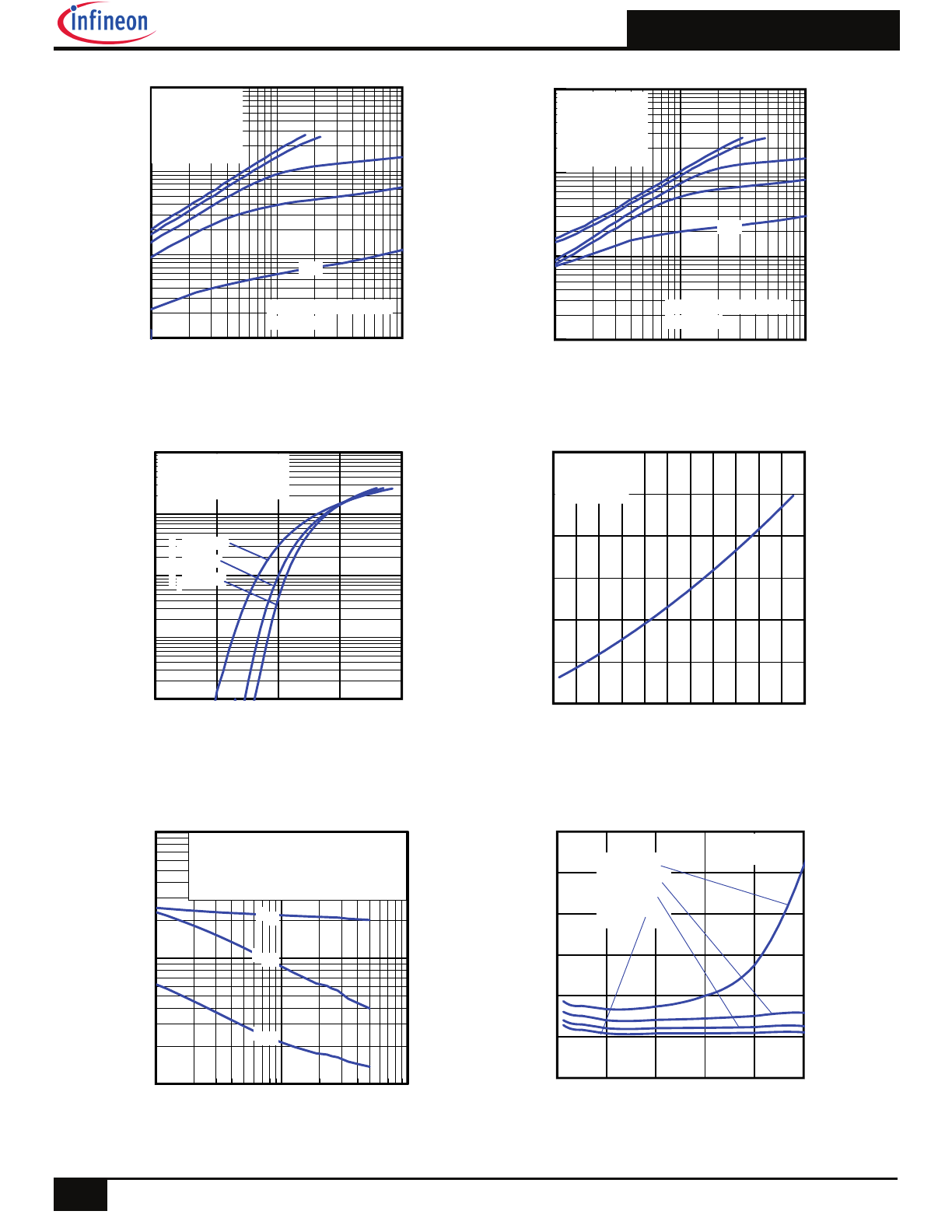
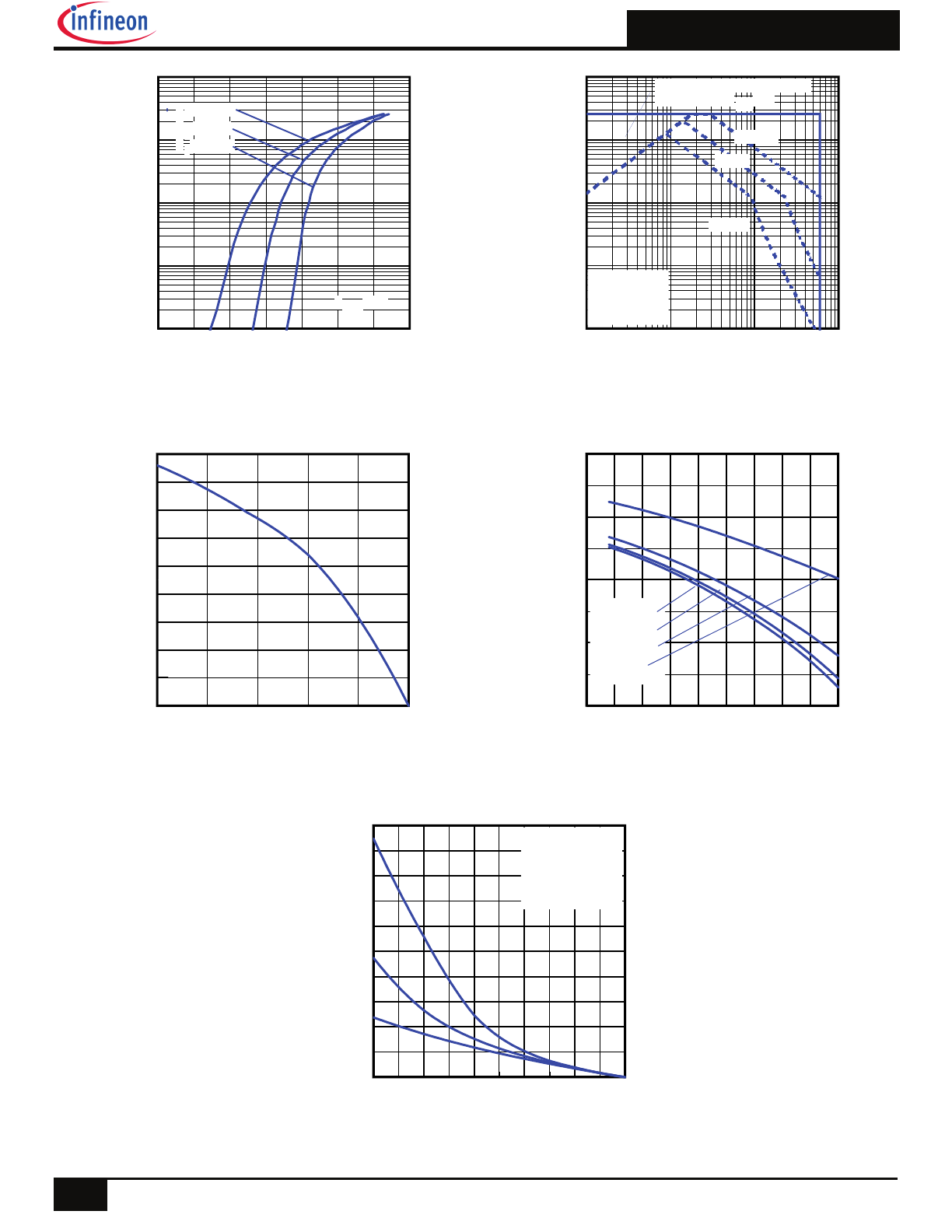
Fig 4. Typical Output Characteristics
Fig 7. Normalized On-Resistance vs. Temperature
Fig 8. Typical Capacitance vs. Drain-to-Source Voltage
Fig 6. Typical Transfer Characteristics
Fig 5. Typical Output Characteristics
0.1
1
10
VDS, Drain-to-Source Voltage (V)
1
10
100
1000
I D
, D
ra
in
-t
o-
S
ou
rc
e
C
ur
re
nt
(
A
)
VGS
TOP 15V
10V
8.0V
7.0V
BOTTOM
6.0V
60µs PULSE WIDTH
Tj = 25°C
6.0V
0.1
1
10
VDS, Drain-to-Source Voltage (V)
1
10
100
1000
I D
, D
ra
in
-t
o-
S
ou
rc
e
C
u
rr
en
t (
A
)
6.0V
60µs PULSE WIDTH
Tj = 150°C
VGS
TOP 15V
10V
8.0V
7.0V
BOTTOM
6.0V
2
4
6
8
10
VGS, Gate-to-Source Voltage (V)
0.1
1
10
100
1000
I D
, D
ra
in
-t
o-
S
ou
rc
e
C
ur
re
nt
(
A
)
TJ = 150°C
TJ = 25°C
TJ = -40°C
VDS = 10V
60µs PULSE WIDTH
-60 -40 -20 0 20 40 60 80 100 120 140 160
TJ , Junction Temperature (°C)
0.5
1.0
1.5
2.0
T
yp
ic
al
R
D
S
(o
n)
(
N
or
m
al
iz
ed
)
ID = 86A
VGS = 10V
1
10
100
VDS, Drain-to-Source Voltage (V)
100
1000
10000
C
, C
ap
ac
ita
nc
e
(p
F
)
VGS = 0V, f = 1 MHZ
Ciss = Cgs + Cgd, C ds SHORTED
Crss = Cgd
Coss = Cds + Cgd
Coss
Crss
Ciss
0
20
40
60
80
100
ID, Drain Current (A)
0
5
10
15
20
25
30
T
yp
ic
al
R
D
S
(o
n)
(
m
)
TJ = 25°C
Vgs = 7.0V
Vgs = 8.0V
Vgs = 10V
Vgs = 15V
Fig 9. Normalized Typical On-Resistance vs. Drain
Current and Gate Voltage
IRF6648TRPbF
5
2017-04-06
Fig 11. Maximum Safe Operating Area
Fig 14. Maximum Avalanche Energy vs. Drain Current
Fig 10. Typical Source-Drain Diode Forward Voltage
Fig 12. Maximum Drain Current vs. Case Temperature
0.0
0.2
0.4
0.6
0.8
1.0
1.2
1.4
VSD, Source-to-Drain Voltage (V)
0
1
10
100
1000
I S
D
, R
ev
er
se
D
ra
in
C
ur
re
nt
(
A
)
TJ = 150°C
TJ = 25°C
TJ = -40°C
VGS = 0V
0
1
10
100
VDS, Drain-to-Source Voltage (V)
0.1
1
10
100
1000
I D
,
D
ra
in
-t
o-
S
ou
rc
e
C
ur
re
nt
(
A
)
OPERATION IN THIS AREA
LIMITED BY R DS(on)
Tc = 25°C
Tj = 150°C
Single Pulse
100µsec
1msec
10msec
25
50
75
100
125
150
TC , Case Temperature (°C)
0
10
20
30
40
50
60
70
80
90
I D
,
D
ra
in
C
ur
re
nt
(
A
)
-75 -50 -25
0
25
50
75 100 125 150
TJ , Temperature ( °C )
2.0
3.0
4.0
5.0
6.0
T
yp
ic
al
V
G
S
(t
h)
, G
at
e
th
re
sh
ol
d
V
ol
ta
ge
(
V
)
ID = 150µA
ID = 250µA
ID = 1.0mA
ID = 1.0A
25
50
75
100
125
150
Starting TJ , Junction Temperature (°C)
0
20
40
60
80
100
120
140
160
180
200
E
A
S
,
S
in
gl
e
P
ul
se
A
va
la
nc
he
E
ne
rg
y
(m
J)
ID
TOP 12A
18A
BOTTOM 34A
Fig 13. Typical Threshold Voltage vs. Junction Temperature
IRF6648TRPbF
6
2017-04-06
Fig 15a. Gate Charge Test Circuit
Fig 15b. Gate Charge Waveform
Fig 16a. Unclamped Inductive Test Circuit
Fig 16b. Unclamped Inductive Waveforms
Fig 17a. Switching Time Test Circuit
Fig 17b. Switching Time Waveforms
IRF6648TRPbF
7
2017-04-06
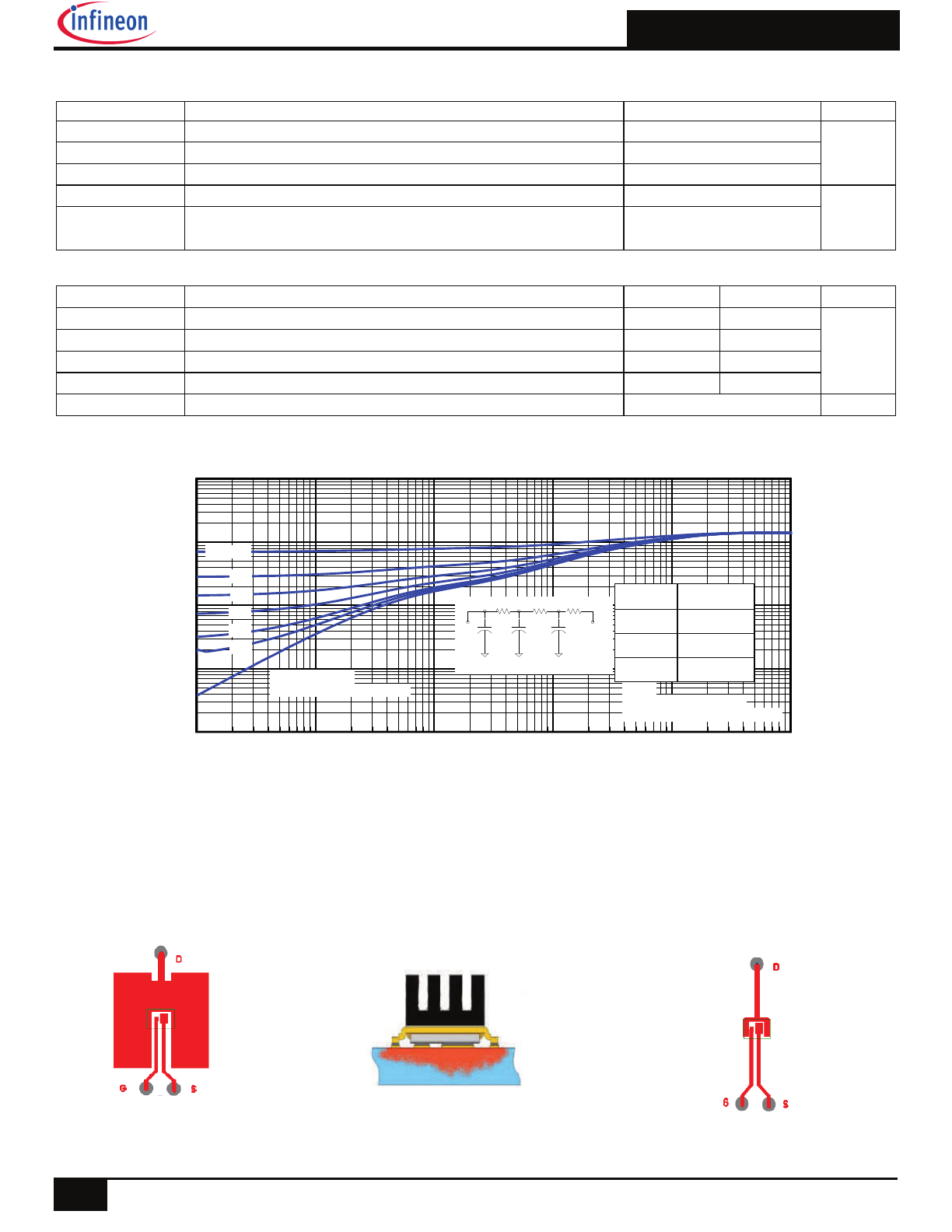
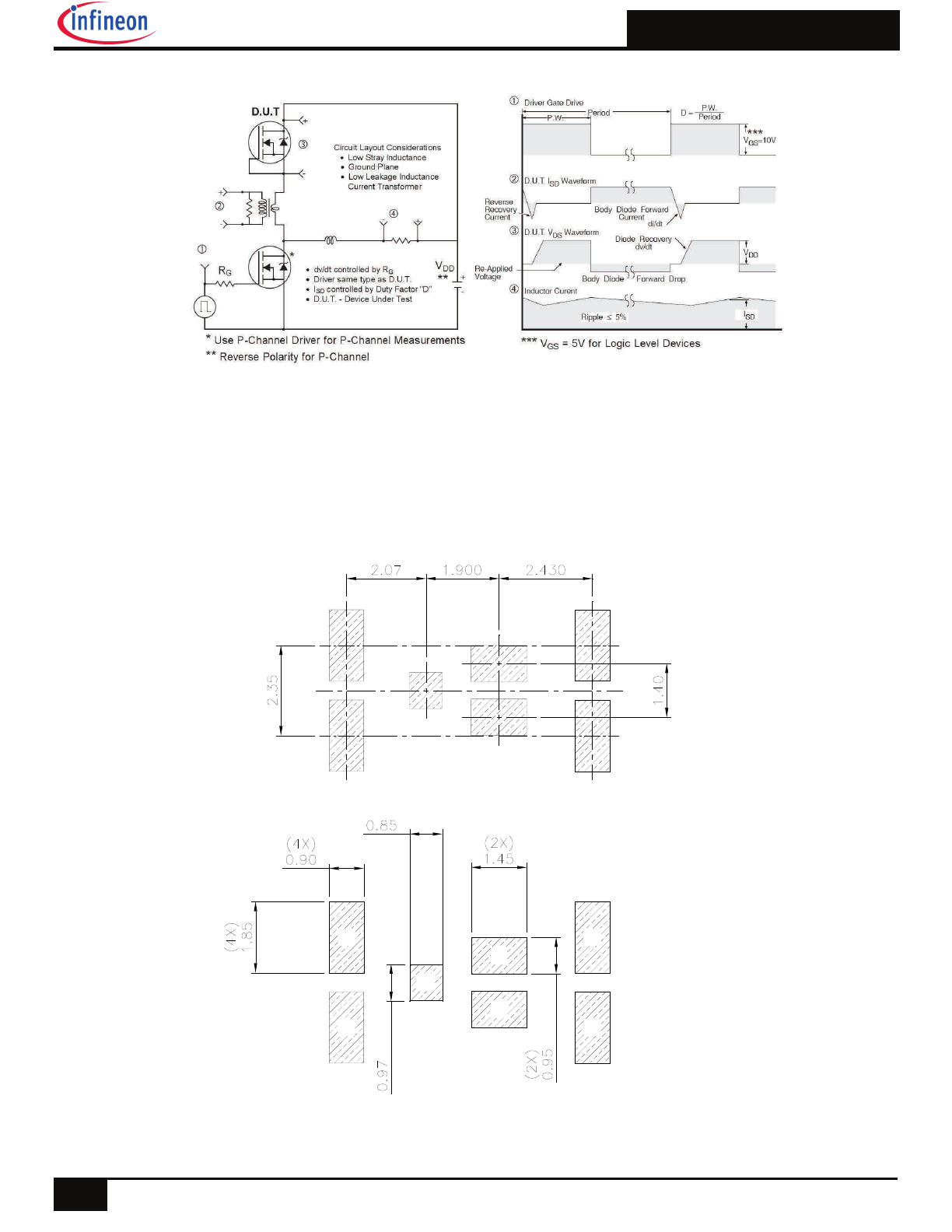
DirectFET™ Substrate and PCB Layout, MN Outline
(Medium Size Can, N-Designation).
Please see DirectFET application note AN-1035 for all details regarding the assembly of DirectFET. This includes all rec-
ommendations for stencil and substrate designs.
Fig 18. Diode Reverse Recovery Test Circuit for HEXFET® Power MOSFETs
G
D
G=GATE
D=DRAIN
S=SOURCE
S
D
D
D
S
IRF6648TRPbF
8
2017-04-06
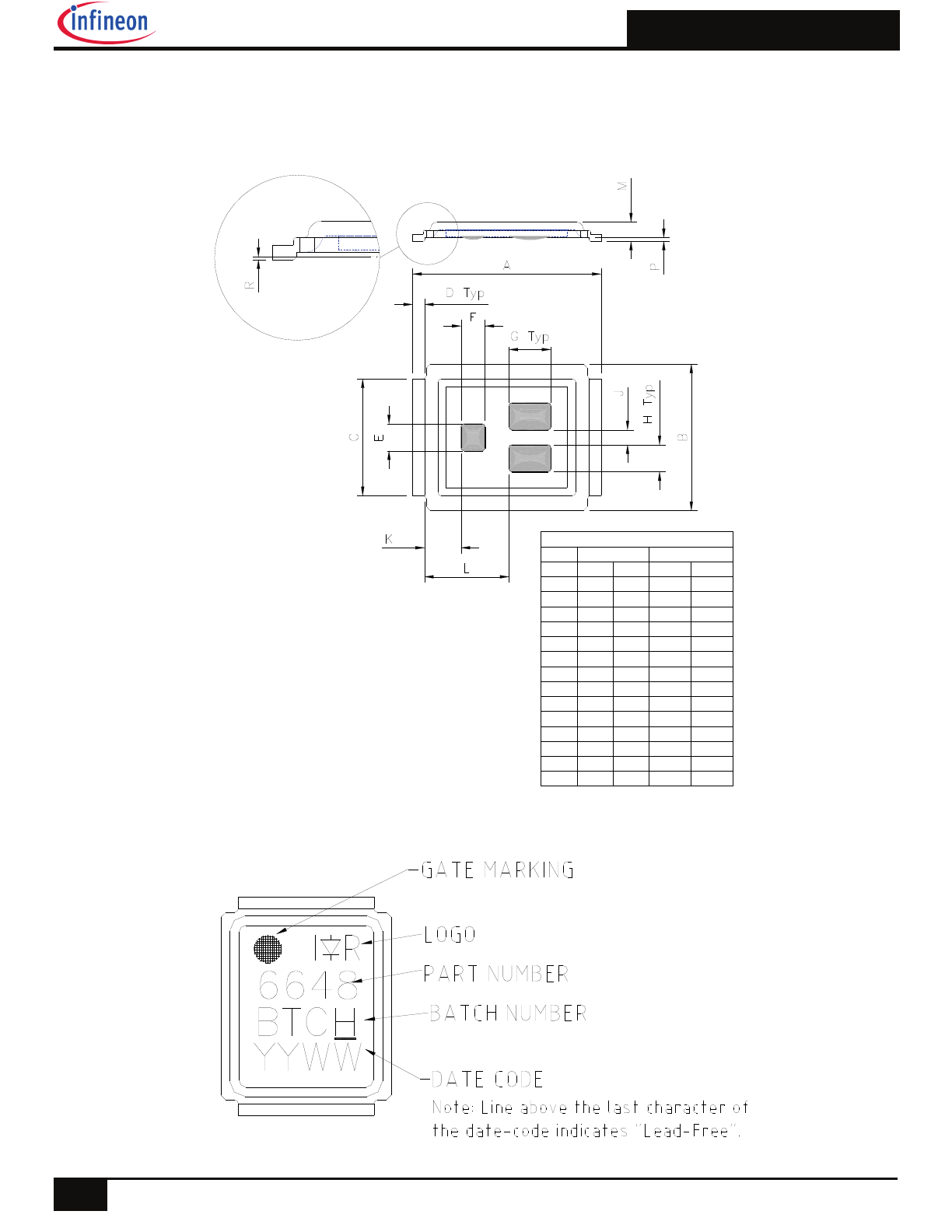
DirectFET™ Outline Dimension, MN Outline
(Medium Size Can, N-Designation).
Please see DirectFET application note AN-1035 for all details regarding the assembly of DirectFET. This includes all
recommendations for stencil and substrate designs.
MAX
0.250
0.201
0.156
0.018
0.036
0.032
0.056
0.036
0.020
0.051
0.115
0.0274
0.0031
0.007
MIN
0.246
0.189
0.152
0.014
0.034
0.031
0.054
0.034
0.019
0.046
0.109
0.0235
0.0008
0.003
MAX
6.35
5.05
3.95
0.45
0.92
0.82
1.42
0.92
0.52
1.29
2.91
0.676
0.080
0.17
MIN
6.25
4.80
3.85
0.35
0.88
0.78
1.38
0.88
0.48
1.16
2.74
0.616
0.020
0.08
CODE
A
B
C
D
E
F
G
H
J
K
L
M
R
P
DIMENSIONS
METRIC
IMPERIAL
DirectFET
™
Part Marking
IRF6648TRPbF
9
2017-04-06
DirectFET
™
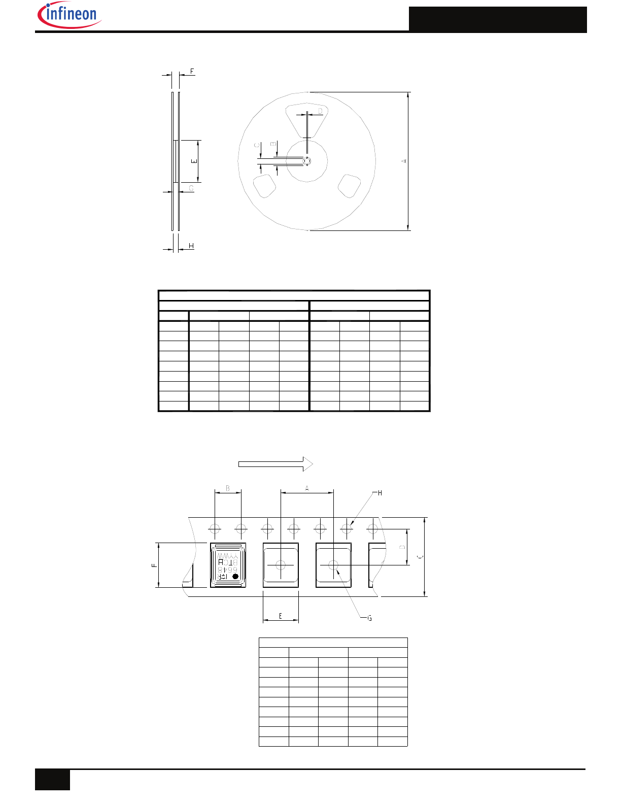
Tape & Reel Dimension (Showing component orientation).
STANDARD OPTION (QTY 4800)
MIN
330.0
20.2
12.8
1.5
100.0
N.C
12.4
11.9
CODE
A
B
C
D
E
F
G
H
MAX
N.C
N.C
13.2
N.C
N.C
18.4
14.4
15.4
MIN
12.992
0.795
0.504
0.059
3.937
N.C
0.488
0.469
MAX
N.C
N.C
0.520
N.C
N.C
0.724
0.567
0.606
METRIC
IMPERIAL
TR1 OPTION (QTY 1000)
IMPERIAL
MIN
6.9
0.75
0.53
0.059
2.31
N.C
0.47
0.47
MAX
N.C
N.C
12.8
N.C
N.C
13.50
12.01
12.01
MIN
177.77
19.06
13.5
1.5
58.72
N.C
11.9
11.9
METRIC
MAX
N.C
N.C
0.50
N.C
N.C
0.53
N.C
N.C
REEL DIMENSIONS
NOTE: Controlling dimensions in mm
Std reel quantity is 4800 parts. (ordered as IRF6648TRPBF). For 1000 parts on 7"
reel, order IRF6648TR1PBF
MIN
7.90
3.90
11.90
5.45
5.10
6.50
1.50
1.50
CODE
A
B
C
D
E
F
G
H
MAX
8.10
4.10
12.30
5.55
5.30
6.70
N.C
1.60
MIN
0.311
0.154
0.469
0.215
0.201
0.256
0.059
0.059
MAX
0.319
0.161
0.484
0.219
0.209
0.264
N.C
0.063
DIMENSIONS
METRIC
IMPERIAL
LOADED TAPE FEED DIRECTION
IRF6648TRPbF
10
2017-04-06
Qualification Information
Qualification Level
Consumer
†
Moisture Sensitivity Level
DirectFET
®
Medium Can
MSL1
(per JEDEC J-STD-020D
†)
RoHS Compliant
Yes
† Applicable version of JEDEC standard at the time of product release.
Revision History
Date Comment
04/06/2017
Changed datasheet with Infineon logo - all pages.
Added Orderable table on page 1.
Corrected PCB layout on page 7
Added Qualification table on page 10.
Added disclaimer on last page.
Published by
Infineon Technologies AG
81726 München, Germany
©
Infineon Technologies AG 2015
All Rights Reserved.
IMPORTANT NOTICE
The information given in this document shall in no event be regarded as a guarantee of conditions or characteristics
(“Beschaffenheitsgarantie”). With respect to any examples, hints or any typical values stated herein and/or any
information regarding the application of the product, Infineon Technologies hereby disclaims any and all warranties and
liabilities of any kind, including without limitation warranties of non-infringement of intellectual property rights of any third
party.
In addition, any information given in this document is subject to customer’s compliance with its obligations stated in this
document and any applicable legal requirements, norms and standards concerning customer’s products and any use of
the product of Infineon Technologies in customer’s applications.
The data contained in this document is exclusively intended for technically trained staff. It is the responsibility of
customer’s technical departments to evaluate the suitability of the product for the intended application and the
completeness of the product information given in this document with respect to such application.
For further information on the product, technology, delivery terms and conditions and prices please contact your nearest
Infineon Technologies office (
www.infineon.com
).
WARNINGS
Due to technical requirements products may contain dangerous substances. For information on the types in question
please contact your nearest Infineon Technologies office.
Except as otherwise explicitly approved by Infineon Technologies in a written document signed by authorized
representatives of Infineon Technologies, Infineon Technologies’ products may not be used in any applications where a
failure of the product or any consequences of the use thereof can reasonably be expected to result in personal injury.