
IRF1407SPbF
IRF1407LPbF
V
DSS
75V
R
DS(on)
0.0078
I
D
100A
Description
Advanced HEXFET® Power MOSFETs from International
Rectifier utilize advanced processing techniques to achieve
extremely low on-resistance per silicon area. This benefit,
combined with the fast switching speed and ruggedized device
design that HEXFET power MOSFETs are well known for,
provides the designer with an extremely efficient and reliable
device for use in a wide variety of applications.
The D2Pak is a surface mount power package capable of
accommodating die sizes up to HEX-4. It provides the highest
power capability and the lowest possible on-resistance in any
existing surface mount package. The D2Pak is suitable for high
current applications because of its low internal connection
resistance and can dissipate up to 2.0W in a typical surface
mount application.
The through-hole version (IRF1407L) is available for low-profile
applications.
1
2016-5-26
Symbol Parameter
Max.
Units
I
D
@ T
C
= 25°C
Continuous Drain Current, V
GS
@ 10V 100
A
I
D
@ T
C
= 100°C
Continuous Drain Current, V
GS
@ 10V 70
I
DM
Pulsed Drain Current 520
P
D
@T
A
= 25°C
Maximum Power Dissipation
3.8
W
P
D
@T
C
= 25°C
Maximum Power Dissipation
200
W
Linear Derating Factor
1.3
W/°C
V
GS
Gate-to-Source Voltage
± 20
V
E
AS
Single Pulse Avalanche Energy (Thermally Limited) 390
mJ
I
AR
Avalanche Current
See Fig.15,16, 12a, 12b
A
E
AR
Repetitive Avalanche Energy
mJ
dv/dt
Peak Diode Recovery dv/dt 4.6
V/ns
T
J
Operating Junction and
-55 to + 175
T
STG
Storage Temperature Range
°C
Soldering Temperature, for 10 seconds (1.6mm from case)
300
Mounting torque, 6-32 or M3 screw
10 lbf•in (1.1N•m)
Absolute Maximum Ratings
Thermal Resistance
Symbol Parameter
Typ.
Max.
Units
R
JC
Junction-to-Case
–––
0.75
°C/W
R
JA
Junction-to-Ambient ( PCB Mount, steady state) –––
40
D2 Pak
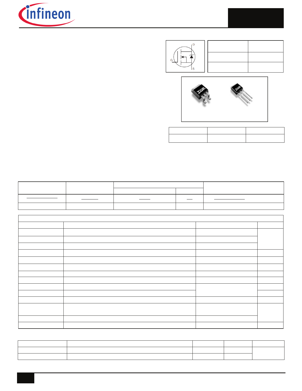
IRF1407SPbF
G D S
Gate Drain Source
Benefits
Advanced Process Technology
Ultra Low On-Resistance
Dynamic dv/dt Rating
175°C Operating Temperature
Fast
Switching
Repetitive Avalanche Allowed up to Tjmax
Lead-Free
S
D
G
S
D
G
D
TO-262 Pak
IRF1407LPbF
Base part number
Package Type
Standard Pack
Form
Quantity
IRF1407LPbF
TO-262
Tube
50
IRF1407LPbF (Obsolete)
IRF1407SPbF
D2-Pak
Tape and Reel Left
800
IRF1407STRLPbF
Orderable Part Number
HEXFET
®
Power MOSFET
IRF1407S/LPbF
2
2016-5-26
Notes:
Repetitive rating; pulse width limited by max. junction temperature. (See fig. 11)
starting T
J
= 25°C, L = 0.13mH, R
G
= 25
, I
AS
= 78A, V
GS
=10V. (See fig. 12)
I
SD
78A, di/dt 320A/µs, V
DD
V
(BR)DSS
, T
J
175°C.
Pulse width
400µs; duty cycle 2%.
C
oss
eff. is a fixed capacitance that gives the same charging time as C
oss
while V
DS
is rising from 0 to 80% V
DSS
.
Calculated continuous current based on maximum allowable junction temperature. Package limitation current is 75A.
Limited by T
Jmax
, see Fig.12a, 12b, 15, 16 for typical repetitive avalanche performance.
Uses IRF1407 data and test conditions.
When mounted on 1" square PCB (FR-4 or G-10 Material). For recommended footprint and soldering techniques refer to
application note #AN-994
Electrical Characteristics @ T
J
= 25°C (unless otherwise specified)
Parameter Min.
Typ.
Max.
Units
Conditions
V
(BR)DSS
Drain-to-Source Breakdown Voltage
75
–––
–––
V V
GS
= 0V, I
D
= 250µA
V
(BR)DSS
/
T
J
Breakdown Voltage Temp. Coefficient
––– 0.09 ––– V/°C Reference to 25°C, I
D
= 1mA
R
DS(on)
Static Drain-to-Source On-Resistance
–––
––– 0.0078
V
GS
= 10V, I
D
= 78A
V
GS(th)
Gate Threshold Voltage
2.0
–––
4.0
V V
DS
= V
GS
, I
D
= 250µA
gfs
Forward Trans conductance
74
–––
–––
S V
DS
= 25V, I
D
= 78A
I
DSS
Drain-to-Source Leakage Current
––– ––– 20
µA
V
DS
=75 V, V
GS
= 0V
––– ––– 250
V
DS
= 60V,V
GS
= 0V,T
J
=150°C
I
GSS
Gate-to-Source Forward Leakage
–––
–––
200
nA
V
GS
= 20V
Gate-to-Source Reverse Leakage
–––
-200
V
GS
= -20V
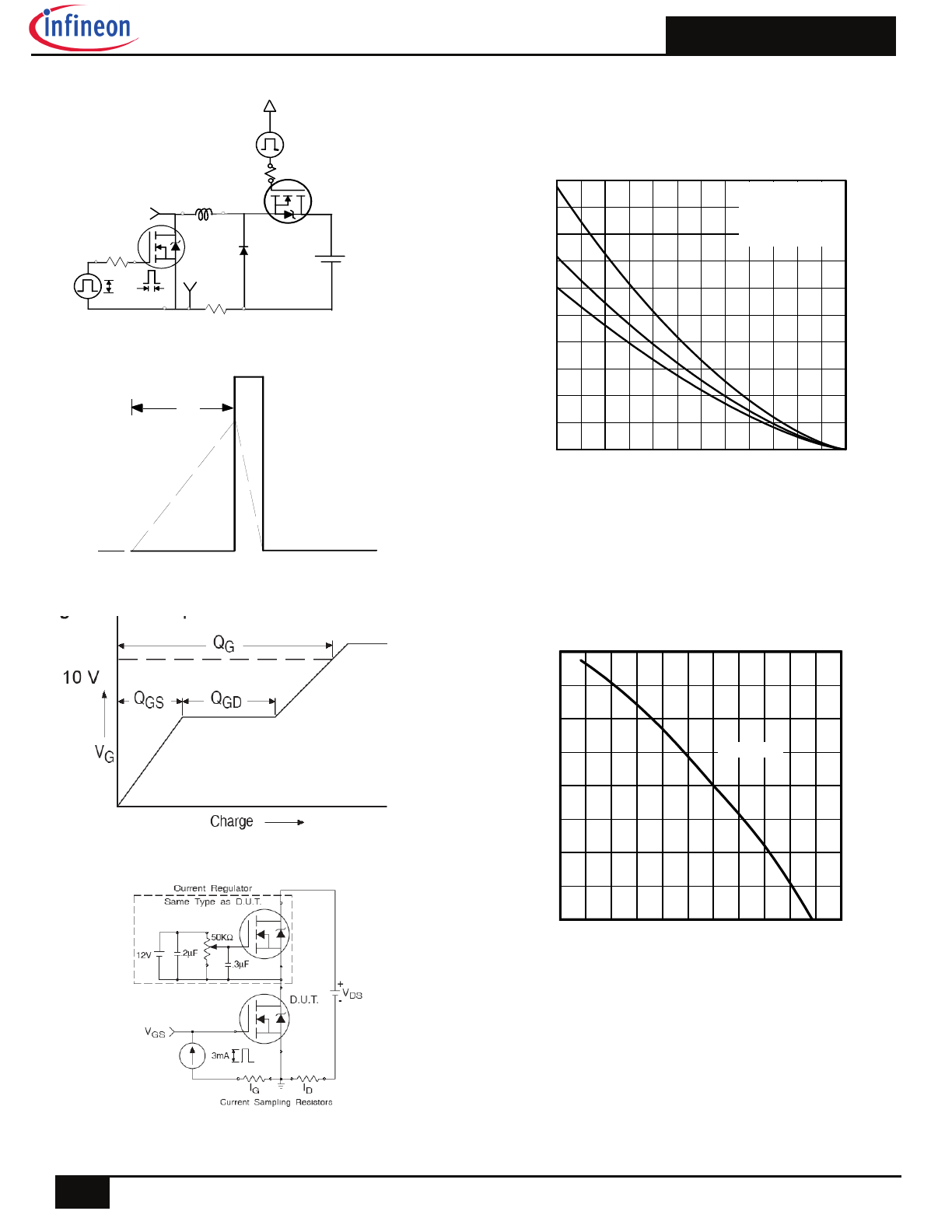
Q
g
Total Gate Charge
–––
160
250
nC
I
D
= 78A
Q
gs
Gate-to-Source Charge
–––
35
52
V
DS
= 60V
Q
gd
Gate-to-Drain Charge
–––
54
81
V
GS
= 10V
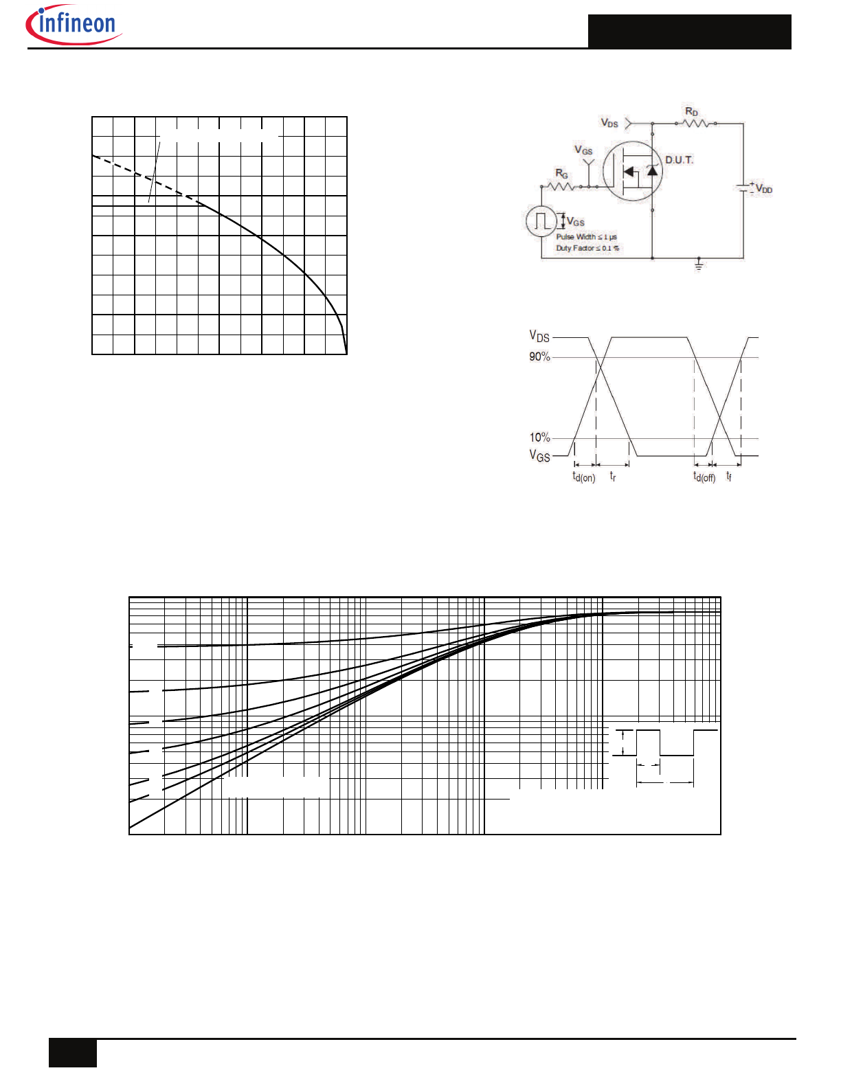
t
d(on)
Turn-On Delay Time
–––
11
–––
ns
V
DD
= 38V
t
r
Rise Time
–––
150
–––
I
D
=78A
t
d(off)
Turn-Off Delay Time
–––
150
–––
R
G
= 2.5
t
f
Fall Time
–––
140
–––
V
GS
= 10V
L
D
Internal Drain Inductance
–––
4.5
–––
nH
Between lead,
6mm (0.25in.)
L
S
Internal Source Inductance
–––
7.5
–––
from package
and center of die contact
C
iss
Input Capacitance
––– 5600 –––
pF
V
GS
= 0V
C
oss
Output Capacitance
–––
890
–––
V
DS
= 25V
C
rss
Reverse Transfer Capacitance
–––
190
–––
ƒ = 1.0kHz, See Fig. 5
C
oss
Output Capacitance
––– 5800 –––
V
GS
= 0V, V
DS
= 1.0V ƒ = 1.0kHz
C
oss
Output Capacitance
–––
560
–––
V
GS
= 0V, V
DS
= 60V ƒ = 1.0kHz
C
oss eff.
Effective Output Capacitance
––– 1100 –––
V
GS
= 0V, V
DS
= 0V to 60V
Source-Drain Ratings and Characteristics
Parameter
Min. Typ. Max. Units
Conditions
I
S
Continuous Source Current
––– ––– 100
A
MOSFET symbol
(Body Diode)
showing the
I
SM
Pulsed Source Current
––– ––– 520
integral reverse
(Body Diode)
p-n junction diode.
V
SD
Diode Forward Voltage
–––
–––
1.3
V T
J
= 25°C,I
S
= 78A,V
GS
= 0V
t
rr
Reverse Recovery Time
–––
110
170
ns T
J
= 25°C ,I
F
= 78A
Q
rr
Reverse Recovery Charge
–––
390
590
nC di/dt = 100A/µs
t
on
Forward Turn-On Time
Intrinsic turn-on time is negligible (turn-on is dominated by L
S
+L
D
)
IRF1407S/LPbF
3
2016-5-26
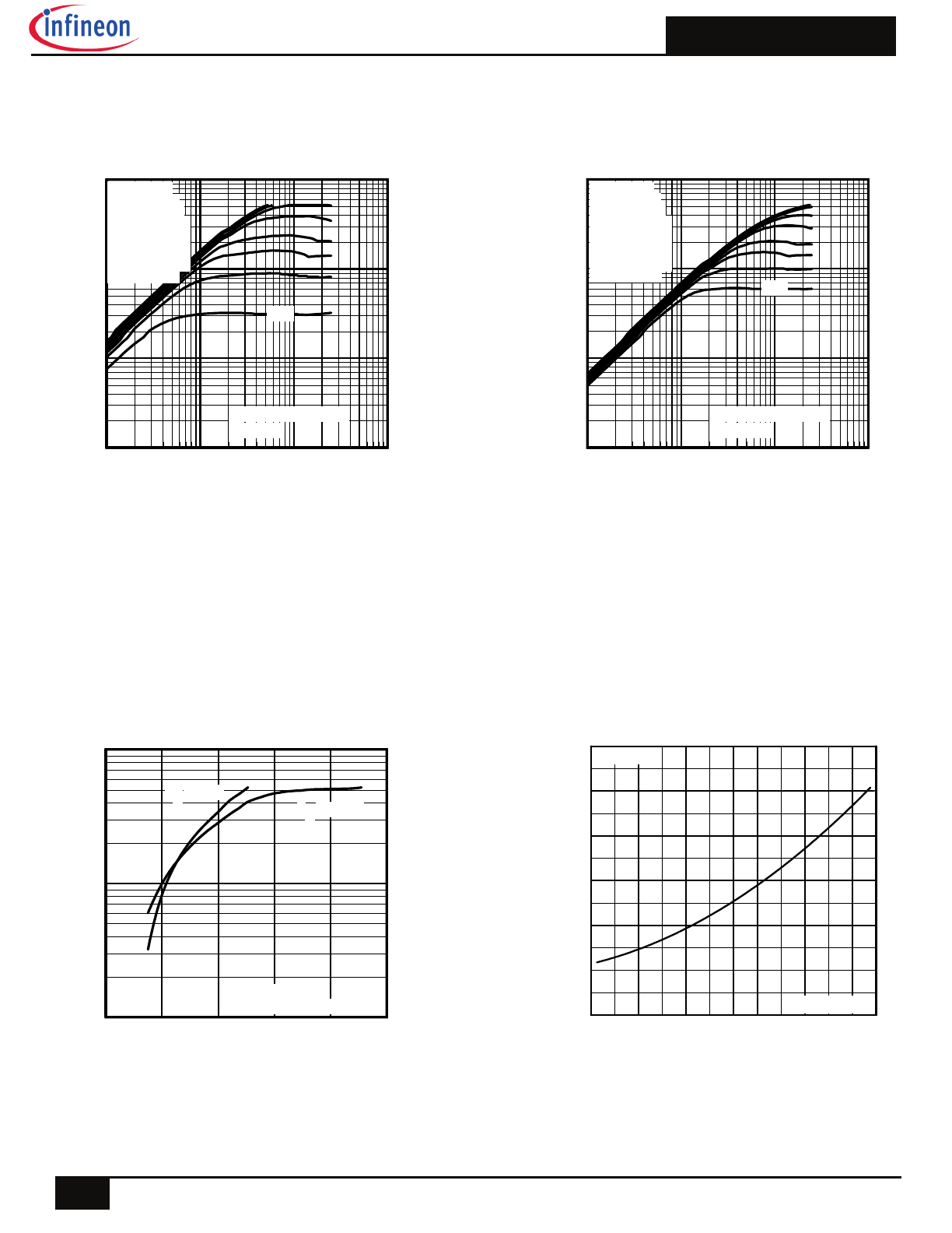
Fig. 2 Typical Output Characteristics
Fig. 3
Typical Transfer Characteristics
Fig. 4 Normalized On-Resistance
vs. Temperature
Fig. 1 Typical Output Characteristics
3.0
5.0
7.0
9.0
11.0
13.0
VGS, Gate-to-Source Voltage (V)
10.00
100.00
1000.00
I D
, D
ra
in
-t
o-
S
ou
rc
e
C
ur
re
nt
)
TJ = 25°C
TJ = 175°C
VDS = 25V
20µs PULSE WIDTH
0.1
1
10
100
VDS, Drain-to-Source Voltage (V)
1
10
100
1000
I D
, D
ra
in
-t
o-
S
ou
rc
e
C
ur
re
nt
(
A
)
4.5V
20µs PULSE WIDTH
Tj = 25°C
VGS
TOP 15V
10V
8.0V
7.0V
6.0V
5.5V
5.0V
BOTTOM 4.5V
0.1
1
10
100
VDS, Drain-to-Source Voltage (V)
1
10
100
1000
I D
, D
ra
in
-t
o-
S
ou
rc
e
C
ur
re
nt
(
A
)
4.5V
20µs PULSE WIDTH
Tj = 175°C
VGS
TOP 15V
10V
8.0V
7.0V
6.0V
5.5V
5.0V
BOTTOM 4.5V
-60
-40
-20
0
20
40
60
80
100
120
140
160
180
0.0
0.5
1.0
1.5
2.0
2.5
3.0
T , Junction Temperature
( C)
R
,
D
ra
in
-to
-S
ou
rc
e O
n R
es
is
ta
nc
e
(N
orm
al
iz
ed
)
J
DS
(o
n
)
°
V
=
I
=
GS
D
10V
130A
IRF1407S/LPbF
4
2016-5-26
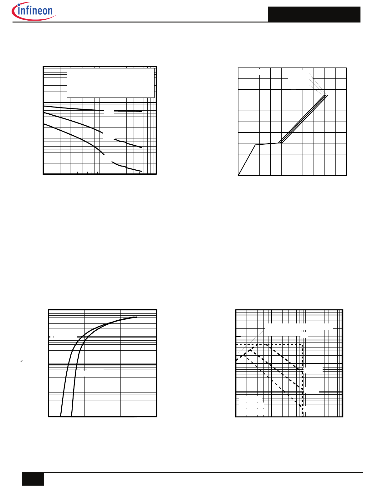
Fig 5. Typical Capacitance vs.
Drain-to-Source Voltage
Fig 8. Maximum Safe Operating Area
Fig. 7 Typical Source-to-Drain Diode
Forward Voltage
1
10
100
VDS, Drain-to-Source Voltage (V)
100
1000
10000
100000
C
, C
ap
ac
ita
nc
e(
pF
)
Coss
Crss
Ciss
VGS = 0V, f = 1 kHZ
Ciss = Cgs + Cgd , Cds SHORTED
Crss = Cgd
Coss = Cds + Cgd
Fig 6. Typical Gate Charge vs.
Gate-to-Source Voltage
1
10
100
1000
VDS , Drain-toSource Voltage (V)
1
10
100
1000
10000
I D
,
D
ra
in
-t
o-
S
ou
rc
e
C
ur
re
nt
(
A
)
Tc = 25°C
Tj = 175°C
Single Pulse
1msec
10msec
OPERATION IN THIS AREA
LIMITED BY R DS(on)
100µsec
0
40
80
120
160
200
0
3
6
9
12
15
Q , Total Gate Charge (nC)
V
, G
a
te
-t
o-
S
o
u
rce
V
o
lta
g
e
(
V
)
G
GS
I
=
D
78A
V
= 15V
DS
V
= 37V
DS
V
= 60V
DS
0.0
1.0
2.0
3.0
VSD, Source-toDrain Voltage (V)
0.10
1.00
10.00
100.00
1000.00
I S
D
,
R
ev
er
se
D
ra
in
C
ur
re
nt
(
A
)
TJ = 25°C
TJ = 175°C
VGS = 0V
IRF1407S/LPbF
5
2016-5-26
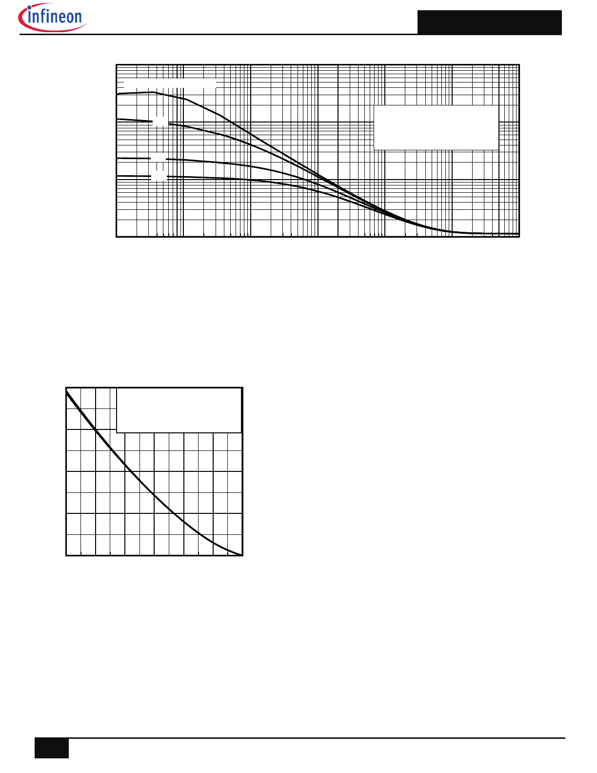
Fig 11. Maximum Effective Transient Thermal Impedance, Junction-to-Case
Fig 9. Maximum Drain Current vs. Case Temperature
Fig 10a. Switching Time Test Circuit
Fig 10b. Switching Time Waveforms
25
50
75
100
125
150
175
0
20
40
60
80
100
120
T , Case Temperature
( C)
I
, D
ra
in
C
ur
re
nt
(
A
)
°
C
D
LIMITED BY PACKAGE
0.01
0.1
1
0.00001
0.0001
0.001
0.01
0.1
1
Notes:
1. Duty f actor D =
t / t
2. Peak T
= P
x Z
+ T
1
2
J
DM
thJC
C
P
t
t
DM
1
2
t , Rectangular Pulse Duration (sec)
T
her
mal
R
es
pons
e
(Z
)
1
th
JC
0.01
0.02
0.05
0.10
0.20
D = 0.50
SINGLE PULSE
(THERMAL RESPONSE)
IRF1407S/LPbF
6
2016-5-26
Fig 14.
Threshold Voltage vs. Temperature
Fig 12c. Maximum Avalanche Energy
vs. Drain Current
Fig 12a. Unclamped Inductive Test Circuit
Fig 12b. Unclamped Inductive Waveforms
R G
IAS
0.01
tp
D.U.T
L
VDS
+
- VDD
DRIVER
A
15V
20V
tp
V
(BR)DSS
I
AS
Fig 13b. Gate Charge Test Circuit
Fig 13a. Gate Charge Waveform
-75 -50 -25
0
25 50 75 100 125 150 175 200
TJ , Temperature ( °C )
1.5
2.0
2.5
3.0
3.5
V
G
S
(t
h)
G
at
e
th
re
sh
ol
d
V
ol
ta
ge
(
V
)
ID = 250µA
25
50
75
100
125
150
175
0
130
260
390
520
650
Starting T , Junction Temperature
( C)
E
,
S
ing
le
P
ul
se
A
val
anc
he
E
ner
gy
(
m
J)
J
AS
°
I D
TOP
BOTTOM
32A
55A
78A
IRF1407S/LPbF
7
2016-5-26
Fig 15. Typical Avalanche Current vs. Pulse width
Notes on Repetitive Avalanche Curves , Figures 15, 16:
(For further info, see AN-1005 at www.infineon.com)
1. Avalanche failures assumption:
Purely a thermal phenomenon and failure occurs at a temperature far in
excess of T
jmax
. This is validated for every part type.
2. Safe operation in Avalanche is allowed as long as T
jmax
is not exceeded.
3. Equation below based on circuit and waveforms shown in Figures 12a, 12b.
4. P
D (ave)
= Average power dissipation per single avalanche pulse.
5. BV = Rated breakdown voltage (1.3 factor accounts for voltage increase
during
avalanche).
6. I
av
= Allowable avalanche current.
7.
T
=
Allowable rise in junction temperature, not to exceed
T
jmax
(assumed as
25°C in Figure 15, 16).
t
av =
Average time in avalanche.
D = Duty cycle in avalanche = t
av
·f
Z
thJC
(D, t
av
) = Transient thermal resistance, see Figures 13)
P
D (ave)
= 1/2 ( 1.3·BV·I
av
) =
T/ Z
thJC
I
av
= 2
T/ [1.3·BV·Z
th
]
E
AS (AR)
= P
D (ave)
·t
av
Fig 16. Maximum Avalanche Energy
vs. Temperature
1.0E-07
1.0E-06
1.0E-05
1.0E-04
1.0E-03
1.0E-02
1.0E-01
tav (sec)
1
10
100
1000
A
va
la
nc
he
C
ur
re
nt
(
A
)
0.05
Duty Cycle = Single Pulse
0.10
Allowed avalanche Current vs
avalanche pulsewidth, tav
assuming
Tj = 25°C due to
avalanche losses
0.01
25
50
75
100
125
150
175
Starting TJ , Junction Temperature (°C)
0
100
200
300
400
E
A
R
,
A
va
la
nc
he
E
ne
rg
y
(m
J)
TOP Single Pulse
BOTTOM 10% Duty Cycle
ID = 78A
IRF1407S/LPbF
8
2016-5-26
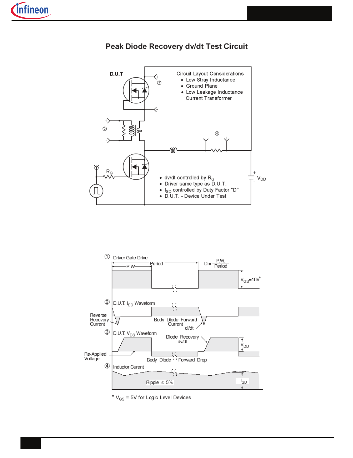
Fig 17. Peak Diode Recovery dv/dt Test Circuit for N-Channel HEXFET® Power MOSFETs
IRF1407S/LPbF
9
2016-5-26
Note: For the most current drawing please refer to Infineon’s web site
www.infineon.com
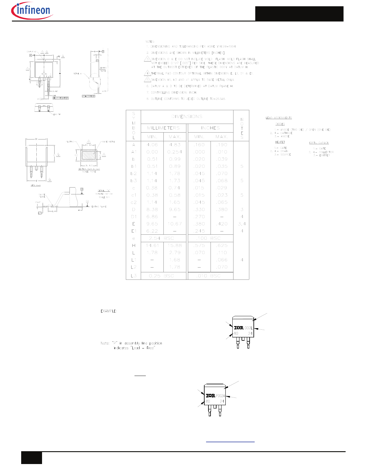
D2-Pak (TO-263AB) Part Marking Information
D2-Pak (TO-263AB) Package Outline (Dimensions are shown in millimeters (inches))
DATE CODE
YEAR 0 = 2000
WEEK 02
A = ASSEMBLY SITE CODE
RECTIFIER
INTERNATIONAL
PART NUMBER
P = DESIGNATES LEAD - FREE
PRODUCT (OPTIONAL)
F530S
IN THE ASSEMBLY LINE "L"
ASSEMBLED ON WW 02, 2000
THIS IS AN IRF530S WITH
LOT CODE 8024
INTERNATIONAL
LOGO
RECTIFIER
LOT CODE
ASSEMBLY
YEAR 0 = 2000
PART NUMBER
DATE CODE
LINE L
WEEK 02
OR
F530S
LOGO
ASSEMBLY
LOT CODE
IRF1407S/LPbF
10
2016-5-26
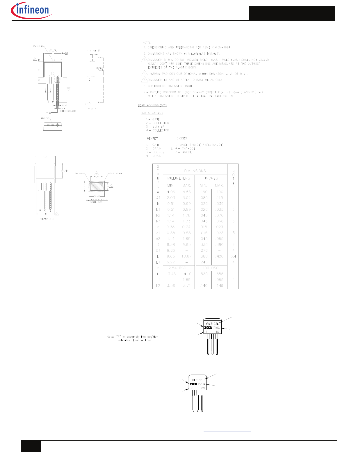
TO-262 Part Marking Information
TO-262 Package Outline (Dimensions are shown in millimeters (inches)
Note: For the most current drawing please refer to Infineon’s web site
www.infineon.com
LOGO
RECTIFIER
INTERNATIONAL
LOT CODE
ASSEMBLY
LOGO
RECTIFIER
INTERNATIONAL
DATE CODE
WEEK 19
YEAR 7 = 1997
PART NUMBER
A = ASSEMBLY SITE CODE
OR
PRODUCT (OPTIONAL)
P = DESIGNATES LEAD-FREE
EXAMPLE: THIS IS AN IRL3103L
LOT CODE 1789
ASSEMBLY
PART NUMBER
DATE CODE
WEEK 19
LINE C
LOT CODE
YEAR 7 = 1997
ASSEMBLED ON WW 19, 1997
IN THE ASSEMBLY LINE "C"