
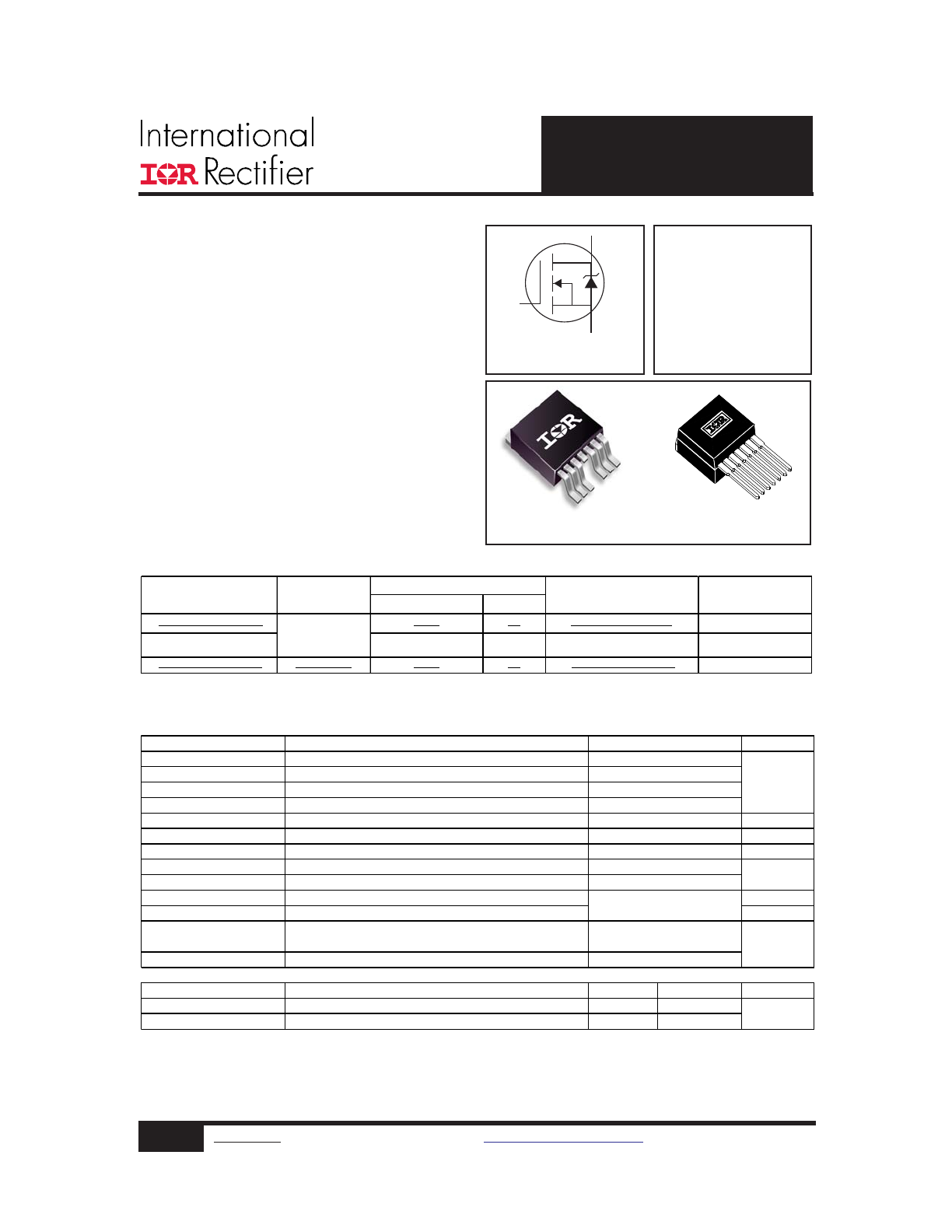
HEXFET
®
Power MOSFET
V
DSS
= 55V
R
DS(on)
= 4.9m
Ω
I
D
= 120A
HEXFET
®
is a registered trademark of International Rectifier.
Description
This HEXFET
®
Power MOSFET utilizes the latest
processing techniques to achieve extremely low
on-resistance per silicon area. Additional features
of this design are a 175°C junction operating
temperature, fast switching speed and improved
repetitive avalanche rating.These features
combine to make this design an extremely efficient
and reliable device for use in a wide variety of
applications.
S
D
G
Features
l
Advanced Process Technology
l
Ultra Low On-Resistance
l
175°C Operating Temperature
l
Fast Switching
l
Repetitive Avalanche Allowed up to Tjmax
l
Lead-Free
S (Pin 2, 3, 5, 6, 7)
G (Pin 1)
D
2
Pak 7 Pin
IRF1405ZS-7PPbF
IRF1405ZL-7PPbF
1
www.irf.com
©
2014 International Rectifier
Submit Datasheet Feedback
October 29, 2014
TO-263CA 7 Pin
Form
Quantity
IRF1405ZS-7PPbF
Tube
50
IRF1405ZS-7PPbF
EOL notice # 289
IRF1405ZS-7PPbF
Tape and Reel Left
800
IRF1405ZSTRL7PP
IRF1405ZL-7PPbF
TO-263CA
Tube
50
IRF1405ZL-7PPbF
EOL notice # 288
Note
Base part number
Package Type
Standard Pack
D
2
Pak-7Pin
Orderable Part Number
Absolute Maximum Ratings
Parameter
Units
I
D
@ T
C
= 25°C
Continuous Drain Current, V
GS
@ 10V (Silicon Limited)
I
D
@ T
C
= 100°C
Continuous Drain Current, V
GS
@ 10V (See Fig. 9)
I
D
@ T
C
= 25°C
Continuous Drain Current, V
GS
@ 10V
(Package L imited)
I
DM
Pulsed Drain Current
c
P
D
@T
C
= 25°C
Maximum Power Dissipation
W
Linear Derating Factor
W/°C
V
GS
Gate-to-Source Voltage
V
E
AS
Single Pulse Avalanche Energy (Thermally Limited)
d
mJ
E
AS
(tested)
Single Pulse Avalanche Energy Tested Value
h
I
AR
Avalanche Current
c
A
E
AR
Repetitive Avalanche Energy
g
mJ
T
J
Operating Junction and
T
STG
Storage Temperature Range
Soldering Temperature, for 10 seconds
Thermal Resistance
Parameter
Typ.
Max.
Units
R
θJC
Junction-to-Case
j
–––
0.65
R
θJA
Junction-to-Ambient (PCB Mount, steady state)
i
–––
40
300(1.6mm from case)
°C
A
°C/W
230
1.5
± 20
250
810
See Fig.12a,12b,15,16
-55 to + 175
Max.
150
100
590
120
2
www.irf.com
©
2014 International Rectifier
Submit Datasheet Feedback
October 29, 2014
IRF1405ZS/L-7PPbF
S
D
G
S
D
G
Static @ T
J
= 25°C (unless otherwise specified)
Parameter
Min.
Typ.
Max.
Units
V
(BR)DSS
Drain-to-Source Breakdown Voltage
55
–––
–––
V
ΔΒV
DSS
/
ΔT
J
Breakdown Voltage Temp. Coefficient
–––
0.054
–––
V/°C
R
DS(on)
SMD
Static Drain-to-Source On-Resistance
–––
3.7
4.9
m
Ω
V
GS(th)
Gate Threshold Voltage
2.0
–––
4.0
V
gfs
Forward Transconductance
150
–––
–––
S
I
DSS
Drain-to-Source Leakage Current
–––
–––
20
–––
–––
250
I
GSS
Gate-to-Source Forward Leakage
–––
–––
200
Gate-to-Source Reverse Leakage
–––
–––
-200
Q
g
Total Gate Charge
–––
150
230
Q
gs
Gate-to-Source Charge
–––
37
–––
Q
gd
Gate-to-Drain ("Miller") Charge
–––
64
–––
t
d(on)
Turn-On Delay Time
–––
16
–––
t
r
Rise Time
–––
140
–––
t
d(off)
Turn-Off Delay Time
–––
170
–––
t
f
Fall Time
–––
130
–––
L
D
Internal Drain Inductance
–––
4.5
–––
nH
Between lead,
6mm (0.25in.)
L
S
Internal Source Inductance
–––
7.5
–––
from package
and center of die contact
C
iss
Input Capacitance
–––
5360
–––
C
oss
Output Capacitance
–––
1310
–––
C
rss
Reverse Transfer Capacitance
–––
340
–––
C
oss
Output Capacitance
–––
6080
–––
C
oss
Output Capacitance
–––
920
–––
C
oss
eff.
Effective Output Capacitance
–––
1700
–––
Diode Characteristics
Parameter
Min.
Typ.
Max.
Units
I
S
Continuous Source Current
(Body Diode)
A
I
SM
Pulsed Source Current
(Body Diode)
c
V
SD
Diode Forward Voltage
–––
–––
1.3
V
t
rr
Reverse Recovery Time
–––
63
95
ns
Q
rr
Reverse Recovery Charge
–––
160
240
nC
pF
nA
nC
μA
ns
–––
–––
150
–––
–––
590
V
DS
= V
GS
, I
D
= 150μA
V
DS
= 55V, V
GS
= 0V
V
DS
= 55V, V
GS
= 0V, T
J
= 125°C
Conditions
V
GS
= 0V, I
D
= 250μA
Reference to 25°C, I
D
= 1mA
V
GS
= 10V, I
D
= 88A
e
T
J
= 25°C, I
F
= 88A, V
DD
= 28V
di/dt = 100A/μs
e
T
J
= 25°C, I
S
= 88A, V
GS
= 0V
e
showing the
integral reverse
p-n junction diode.
V
GS
= 0V, V
DS
= 1.0V, ƒ = 1.0MHz
V
GS
= 10V
d
MOSFET symbol
V
GS
= 0V
V
DS
= 25V
V
GS
= 0V, V
DS
= 44V, ƒ = 1.0MHz
Conditions
V
GS
= 0V, V
DS
= 0V to 44V
ƒ = 1.0MHz, See Fig. 5
R
G
= 5.0
Ω
I
D
= 88A
V
DS
= 25V, I
D
= 88A
V
DD
= 28V
I
D
= 88A
V
GS
= 20V
V
GS
= -20V
V
DS
= 44V
V
GS
= 10V
e
Notes:
Repetitive rating; pulse width limited by max. junction temperature. (See fig. 11).
Limited by T
Jmax
, starting T
J
= 25°C, L=0.064mH, R
G
= 25
Ω, I
AS
= 88A, V
GS
=10V.
Part not recommended for use above this value.
Pulse width ≤ 1.0ms; duty cycle ≤ 2%.
C
oss
eff. is a fixed capacitance that gives the same charging time as C
oss
while V
DS
is rising from 0 to 80% V
DSS
.
Limited by T
Jmax
, see Fig.12a, 12b, 15, 16 for typical repetitive avalanche performance.
This value determined from sample failure population. 100% tested to this value in production.
This is applied to D
2
Pak, when mounted on 1" square PCB ( FR-4 or G-10 Material ). For recommended footprint and
soldering techniques refer to application note #AN-994.
R
θ
is measured at T
J
of approximately 90°C.
Solder mounted on IMS substrate.
3
www.irf.com
©
2014 International Rectifier
Submit Datasheet Feedback
October 29, 2014
IRF1405ZS/L-7PPbF
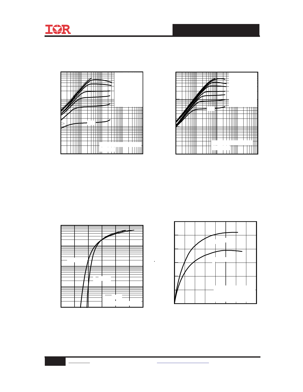
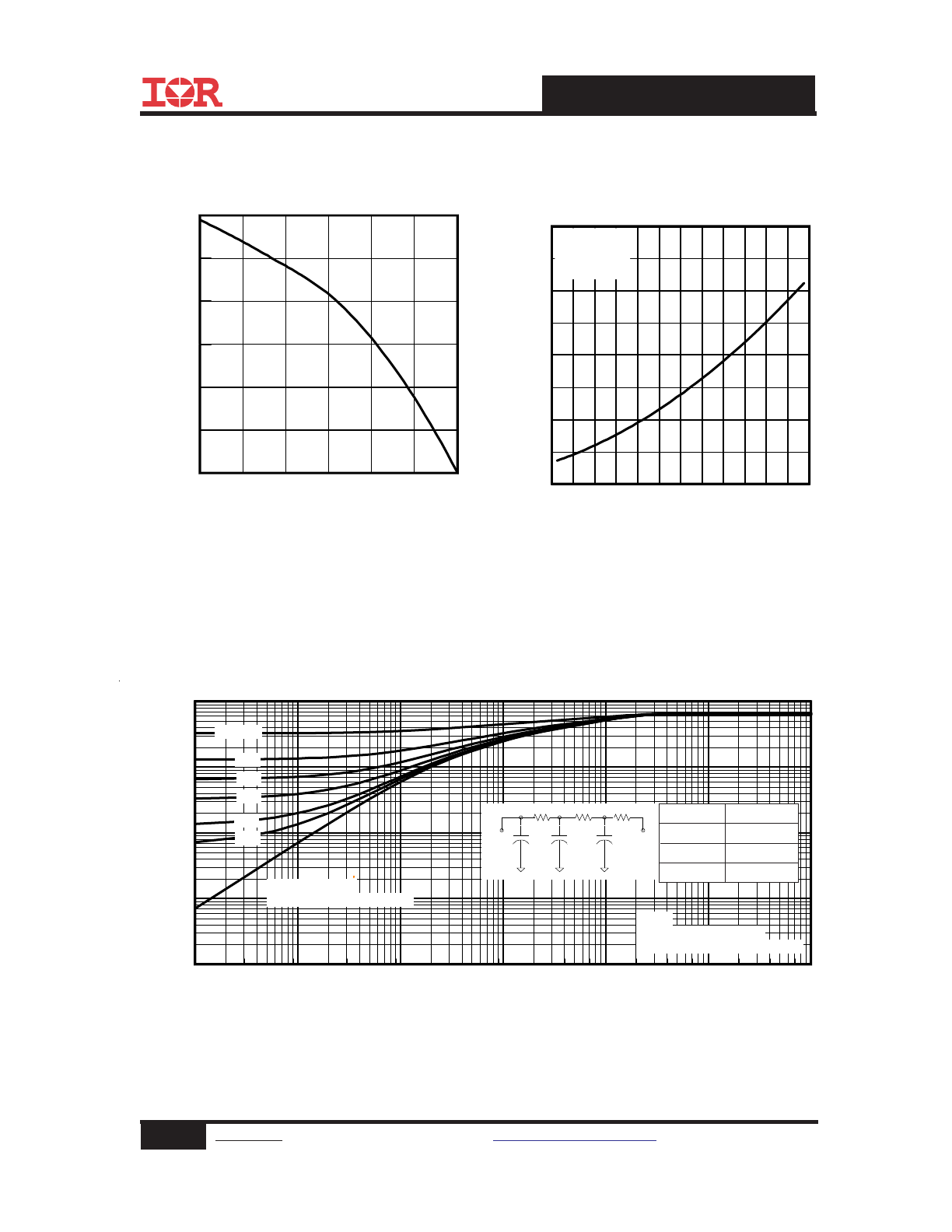
Fig 2. Typical Output Characteristics
Fig 1. Typical Output Characteristics
Fig 3. Typical Transfer Characteristics
Fig 4. Typical Forward Transconductance
vs. Drain Current
0.1
1
10
100
1000
VDS, Drain-to-Source Voltage (V)
1
10
100
1000
I D
, D
ra
in
-t
o-
S
ou
rc
e
C
ur
re
nt
(
A
)
VGS
TOP
15V
10V
8.0V
7.0V
6.0V
5.5V
5.0V
BOTTOM
4.5V
≤60μs PULSE WIDTH
Tj = 25°C
4.5V
0
2
4
6
8
10
12
VGS, Gate-to-Source Voltage (V)
0.1
1
10
100
1000
I D
, D
ra
in
-t
o-
S
ou
rc
e
C
ur
re
nt
(
Α
)
TJ = 25°C
TJ = 175°C
VDS = 25V
≤60μs PULSE WIDTH
0.1
1
10
100
1000
VDS, Drain-to-Source Voltage (V)
1
10
100
1000
I D
, D
ra
in
-t
o-
S
ou
rc
e
C
ur
re
nt
(
A
)
4.5V
≤60μs PULSE WIDTH
Tj = 175°C
VGS
TOP
15V
10V
8.0V
7.0V
6.0V
5.5V
5.0V
BOTTOM
4.5V
0
25
50
75
100 125 150 175 200
ID,Drain-to-Source Current (A)
0
25
50
75
100
125
150
G
fs
, F
or
w
ar
d
T
ra
ns
co
nd
uc
ta
nc
e
(S
)
TJ = 25°C
TJ = 175°C
VDS = 10V
300μs PULSE WIDTH
4
www.irf.com
©
2014 International Rectifier
Submit Datasheet Feedback
October 29, 2014
IRF1405ZS/L-7PPbF
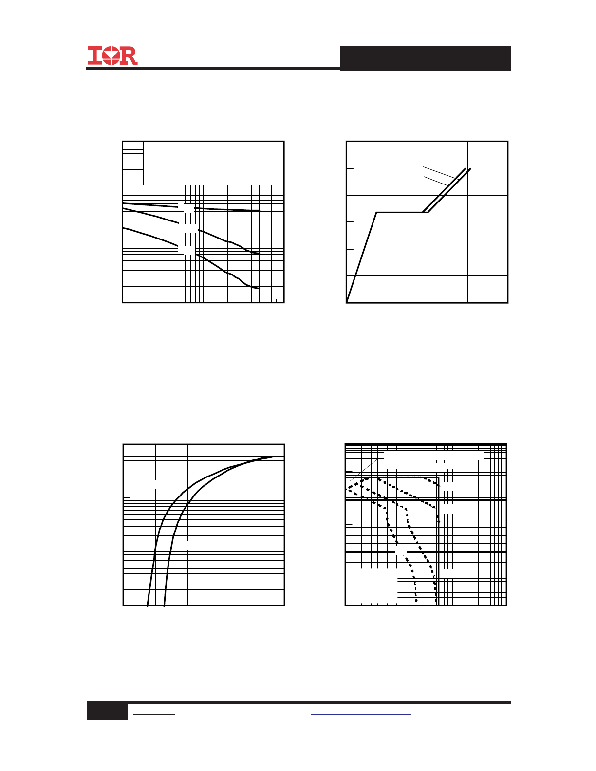
Fig 8. Maximum Safe Operating Area
Fig 6. Typical Gate Charge vs.
Gate-to-Source Voltage
Fig 5. Typical Capacitance vs.
Drain-to-Source Voltage
Fig 7. Typical Source-Drain Diode
Forward Voltage
0
50
100
150
200
QG Total Gate Charge (nC)
0.0
2.0
4.0
6.0
8.0
10.0
12.0
V
G
S
, G
at
e-
to
-S
ou
rc
e
V
ol
ta
ge
(
V
)
VDS= 44V
VDS= 28V
ID= 88A
1
10
100
VDS, Drain-to-Source Voltage (V)
100
1000
10000
100000
C
, C
ap
ac
ita
nc
e(
pF
)
VGS = 0V, f = 1 MHZ
Ciss = Cgs + Cgd, C ds SHORTED
Crss = Cgd
Coss = Cds + Cgd
Coss
Crss
Ciss
0.0
0.5
1.0
1.5
2.0
2.5
VSD, Source-to-Drain Voltage (V)
1
10
100
1000
I S
D
, R
ev
er
se
D
ra
in
C
ur
re
nt
(
A
)
TJ = 25°C
TJ = 175°C
VGS = 0V
1
10
100
1000
VDS, Drain-to-Source Voltage (V)
0.01
0.1
1
10
100
1000
10000
I D
,
D
ra
in
-t
o-
S
ou
rc
e
C
ur
re
nt
(
A
)
OPERATION IN THIS AREA
LIMITED BY R DS(on)
Tc = 25°C
Tj = 175°C
Single Pulse
100μsec
1msec
10msec
DC
5
www.irf.com
©
2014 International Rectifier
Submit Datasheet Feedback
October 29, 2014
IRF1405ZS/L-7PPbF
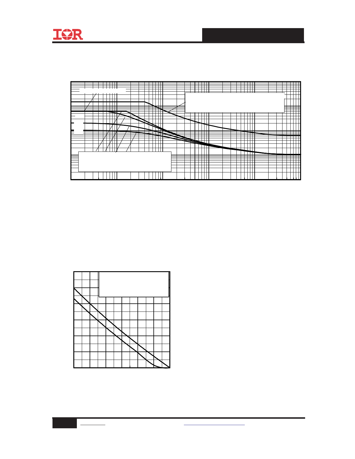
Fig 11. Maximum Effective Transient Thermal Impedance, Junction-to-Case
Fig 9. Maximum Drain Current vs.
Case Temperature
Fig 10. Normalized On-Resistance
vs. Temperature
-60 -40 -20 0 20 40 60 80 100 120 140 160 180
TJ , Junction Temperature (°C)
0.5
1.0
1.5
2.0
2.5
R
D
S
(o
n)
,
D
ra
in
-t
o-
S
ou
rc
e
O
n
R
es
is
ta
nc
e
(
N
or
m
al
iz
ed
)
ID = 88A
VGS = 10V
1E-006
1E-005
0.0001
0.001
0.01
0.1
1
t1 , Rectangular Pulse Duration (sec)
0.0001
0.001
0.01
0.1
1
T
he
rm
al
R
es
po
ns
e
(
Z
th
JC
)
0.20
0.10
D = 0.50
0.02
0.01
0.05
SINGLE PULSE
( THERMAL RESPONSE )
Notes:
1. Duty Factor D = t1/t2
2. Peak Tj = P dm x Zthjc + Tc
Ri (°C/W)
τi (sec)
0.1707 0.000235
0.1923 0.000791
0.2885 0.008193
τ
J
τ
J
τ
1
τ
1
τ
2
τ
2
τ
3
τ
3
R
1
R
1
R
2
R
2
R
3
R
3
τ
τ
C
Ci i
/Ri
Ci=
τi/Ri
25
50
75
100
125
150
175
TC , Case Temperature (°C)
0
25
50
75
100
125
150
I D
,
D
ra
in
C
ur
re
nt
(
A
)
6
www.irf.com
©
2014 International Rectifier
Submit Datasheet Feedback
October 29, 2014
IRF1405ZS/L-7PPbF
Q
G
Q
GS
Q
GD
V
G
Charge
D.U.T.
V
DS
I
D
I
G
3mA
V
GS
.3
μF
50K
Ω
.2
μF
12V
Current Regulator
Same Type as D.U.T.
Current Sampling Resistors
+
-
10 V
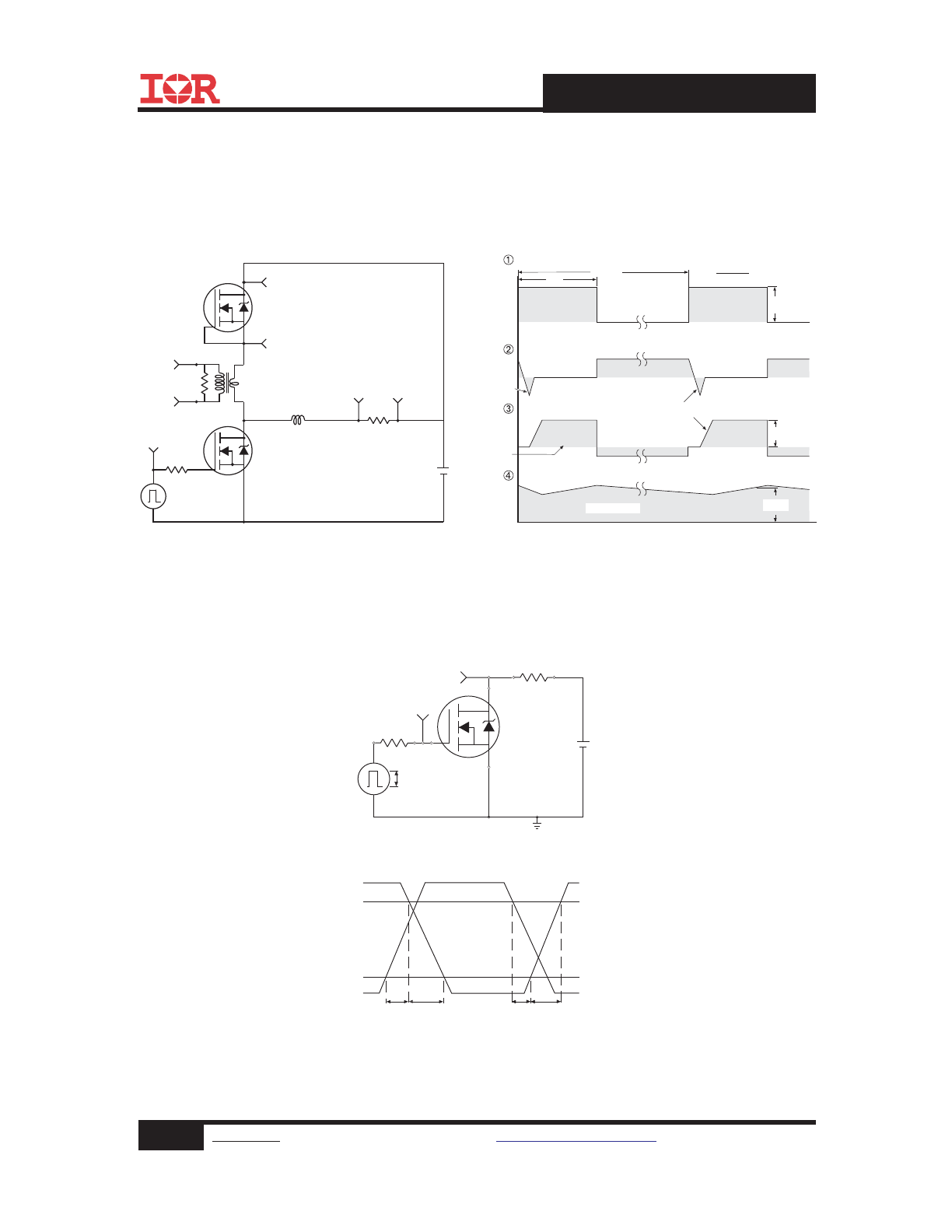
Fig 13b. Gate Charge Test Circuit
Fig 13a. Basic Gate Charge Waveform
Fig 12c. Maximum Avalanche Energy
vs. Drain Current
Fig 12b. Unclamped Inductive Waveforms
Fig 12a. Unclamped Inductive Test Circuit
tp
V
(BR)DSS
I
AS
Fig 14. Threshold Voltage vs. Temperature
RG
IAS
0.01
Ω
tp
D.U.T
L
VDS
+
- VDD
DRIVER
A
15V
20V
V
GS
25
50
75
100
125
150
175
Starting TJ , Junction Temperature (°C)
0
200
400
600
800
1000
E
A
S
,
S
in
gl
e
P
ul
se
A
va
la
nc
he
E
ne
rg
y
(m
J)
ID
TOP 14A
23A
BOTTOM 88A
-75 -50 -25
0
25 50 75 100 125 150 175 200
TJ , Temperature ( °C )
1.0
1.5
2.0
2.5
3.0
3.5
4.0
4.5
V
G
S
(t
h)
G
at
e
th
re
sh
ol
d
V
ol
ta
ge
(
V
)
ID = 150μA
ID = 250μA
ID = 1.0mA
ID = 1.0A
7
www.irf.com
©
2014 International Rectifier
Submit Datasheet Feedback
October 29, 2014
IRF1405ZS/L-7PPbF
Fig 15. Typical Avalanche Current vs.Pulsewidth
Fig 16. Maximum Avalanche Energy
vs. Temperature
Notes on Repetitive Avalanche Curves , Figures 15, 16:
(For further info, see AN-1005 at www.irf.com)
1. Avalanche failures assumption:
Purely a thermal phenomenon and failure occurs at a
temperature far in excess of T
jmax
. This is validated for
every part type.
2. Safe operation in Avalanche is allowed as long asT
jmax
is
not exceeded.
3. Equation below based on circuit and waveforms shown in
Figures 12a, 12b.
4. P
D (ave)
= Average power dissipation per single
avalanche pulse.
5. BV = Rated breakdown voltage (1.3 factor accounts for
voltage increase during avalanche).
6. I
av
= Allowable avalanche current.
7.
ΔT
=
Allowable rise in junction temperature, not to exceed
T
jmax
(assumed as 25°C in Figure 15, 16).
t
av =
Average time in avalanche.
D = Duty cycle in avalanche = t
av
·f
Z
thJC
(D, t
av
) = Transient thermal resistance, see figure 11)
P
D (ave)
= 1/2 ( 1.3·BV·I
av
) =
DT/ Z
thJC
I
av
=
2
DT/ [1.3·BV·Z
th
]
E
AS (AR)
= P
D (ave)
·t
av
25
50
75
100
125
150
175
Starting TJ , Junction Temperature (°C)
0
50
100
150
200
250
300
E
A
R
,
A
va
la
nc
he
E
ne
rg
y
(m
J)
TOP Single Pulse
BOTTOM 1% Duty Cycle
ID = 88A
1.0E-06
1.0E-05
1.0E-04
1.0E-03
1.0E-02
1.0E-01
tav (sec)
0.1
1
10
100
1000
A
va
la
nc
he
C
ur
re
nt
(
A
)
0.05
Duty Cycle = Single Pulse
0.10
Allowed avalanche Current vs avalanche
pulsewidth, tav, assuming
ΔΤj = 25°C and
Tstart = 150°C.
0.01
Allowed avalanche Current vs avalanche
pulsewidth, tav, assuming
ΔTj = 150°C and
Tstart =25°C (Single Pulse)
8
www.irf.com
©
2014 International Rectifier
Submit Datasheet Feedback
October 29, 2014
IRF1405ZS/L-7PPbF
Fig 17.
Peak Diode Recovery dv/dt Test Circuit for N-Channel
HEXFET
®
Power MOSFETs
Circuit Layout Considerations
• Low Stray Inductance
• Ground Plane
• Low Leakage Inductance
Current Transformer
P.W.
Period
di/dt
Diode Recovery
dv/dt
Ripple
≤ 5%
Body Diode Forward Drop
Re-Applied
Voltage
Reverse
Recovery
Current
Body Diode Forward
Current
V
GS
=10V
V
DD
I
SD
Driver Gate Drive
D.U.T. I
SD
Waveform
D.U.T. V
DS
Waveform
Inductor Curent
D =
P.W.
Period
*
V
GS
= 5V for Logic Level Devices
*
+
-
+
+
+
-
-
-
R
G
V
DD
• dv/dt controlled by R
G
• Driver same type as D.U.T.
• I
SD
controlled by Duty Factor "D"
• D.U.T. - Device Under Test
D.U.T
V
DS
90%
10%
V
GS
t
d(on)
t
r
t
d(off)
t
f
V
DS
Pulse Width ≤ 1 µs
Duty Factor ≤ 0.1 %
R
D
V
GS
R
G
D.U.T.
10V
+
-
V
DD
Fig 18a. Switching Time Test Circuit
Fig 18b. Switching Time Waveforms
9
www.irf.com
©
2014 International Rectifier
Submit Datasheet Feedback
October 29, 2014
IRF1405ZS/L-7PPbF
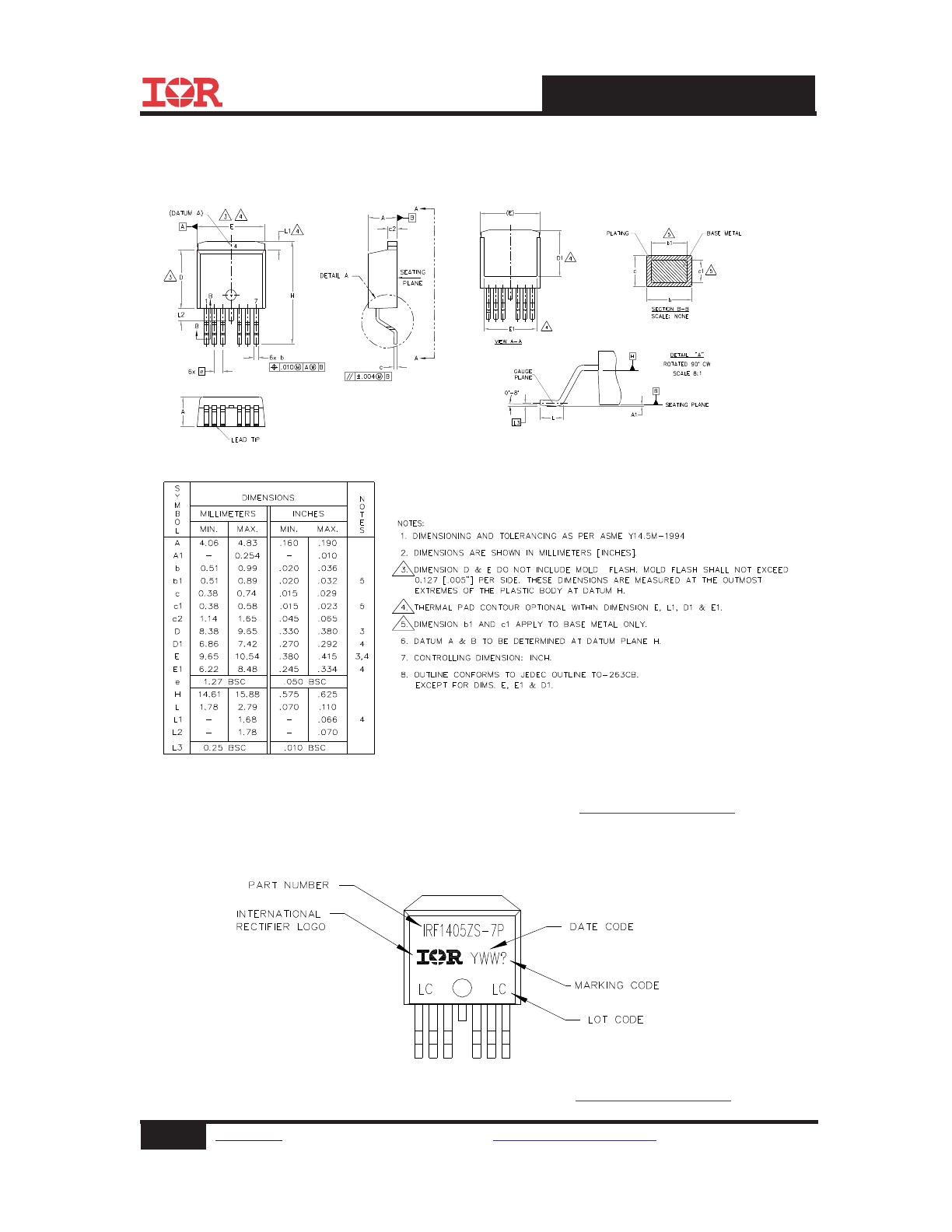
D
2
Pak - 7 Pin Package Outline
Dimensions are shown in millimeters (inches)
Note: For the most current drawing please refer to IR website at:
http://www.irf.com/package/
D
2
Pak - 7 Pin Part Marking Information
Note: For the most current drawing please refer to IR website at:
http://www.irf.com/package/
10
www.irf.com
©
2014 International Rectifier
Submit Datasheet Feedback
October 29, 2014
IRF1405ZS/L-7PPbF
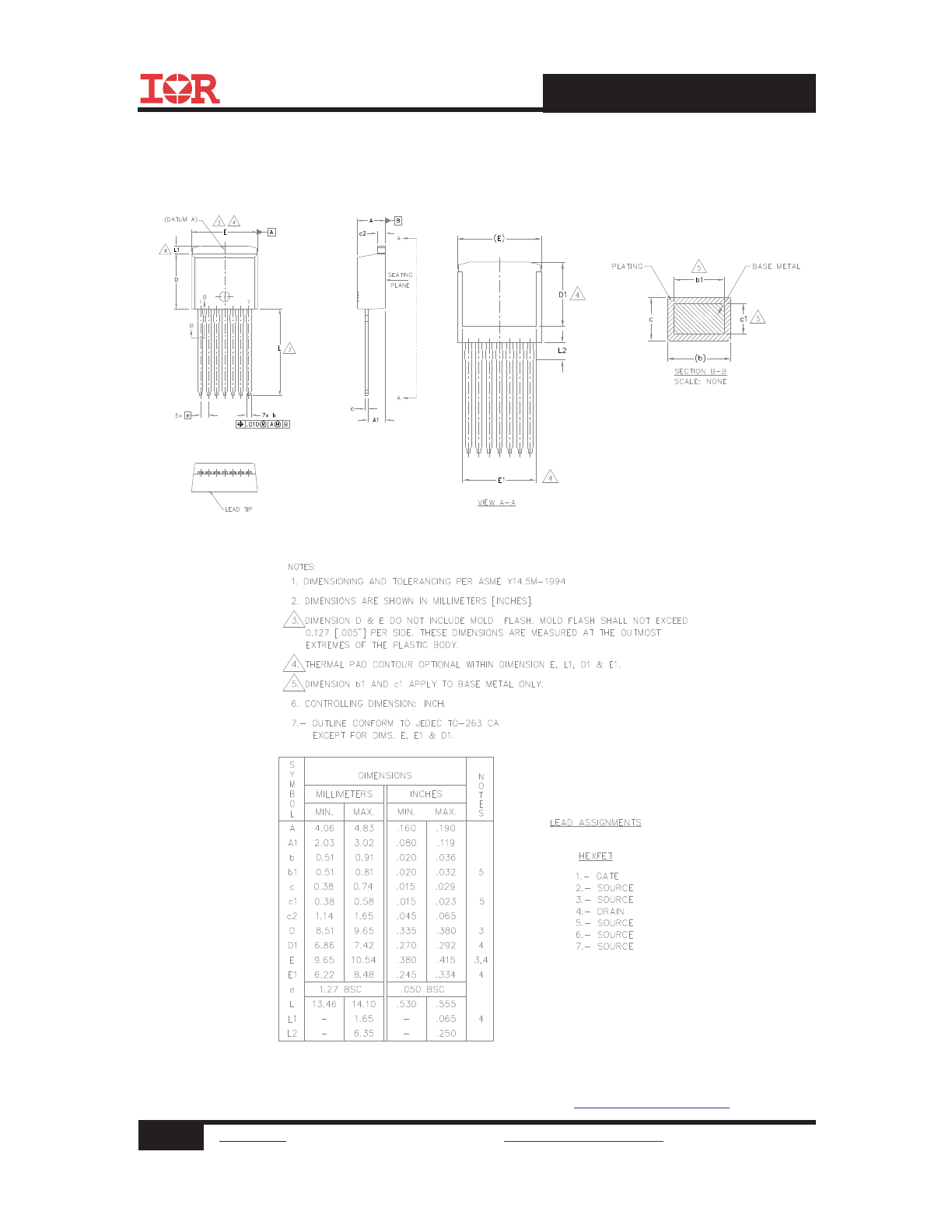
TO-263CA 7 Pin Long Leads Package Outline
Dimensions are shown in millimeters (inches)
Note: For the most current drawing please refer to IR website at:
http://www.irf.com/package/