
Rev 4.0
1
PD-97528
IR3856MPbF
Features
•
Greater than 95% Maximum Efficiency
•
Wide Input Voltage Range 1.5V to 21V
•
Wide Output Voltage Range 0.7V to 0.9*Vin
•
Continuous 6A Load Capability
•
Integrated Bootstrap-diode
•
High Bandwidth E/A for excellent transient
performance
•
Programmable Switching Frequency up to 1.5MHz
•
Programmable Over Current Protection
•
Over Voltage Protection
•
Dedicated input for output voltage monitoring
•
Programmable PGood output
•
Hiccup Current Limit
•
Precision Reference Voltage (0.7V, +/-1%)
•
Programmable Soft-Start
•
Enable Input with Voltage Monitoring Capability
•
Enhanced Pre-Bias Start-up
•
Seq input for Tracking applications
•
External Synchronization
•
-40
o
C to 125
o
C operating junction temperature
•
Thermal Protection
•
4mm x 5mm Power QFN Package
•
Halogen Free, Lead Free and RoHS compliant
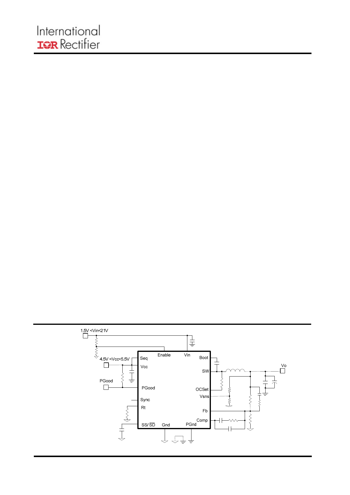
Fig. 1. Typical application diagram
Description
The IR3856 SupIRBuck
TM
is an easy-to-use, fully
integrated and highly efficient DC/DC
synchronous Buck regulator. The MOSFETs co-
packaged with the on-chip PWM controller make
IR3856 a space-efficient solution, providing
accurate power delivery for low output voltage
applications.
IR3856 is a versatile regulator which offers
programmability of start up time, switching
frequency and current limit while operating in
wide input and output voltage range.
The switching frequency is programmable from
250kHz to 1.5MHz for an optimum solution.
It also features important protection functions,
such as Pre-Bias startup, hiccup current limit and
thermal shutdown to give required system level
security in the event of fault conditions.
HIGHLY EFFICIENT
INTEGRATED 6A, SYNCHRONOUS BUCK REGULATOR
SupIRBuck
TM
•
Distributed Point of Load Power Architectures
•
Netcom Applications
•
Computing Peripheral Voltage Regulators
•
General DC-DC Converters
Applications
•
Server Applications
•
Storage Applications
•
Embedded Telecom Systems
Rev 4.0
2
PD-97528
IR3856MPbF
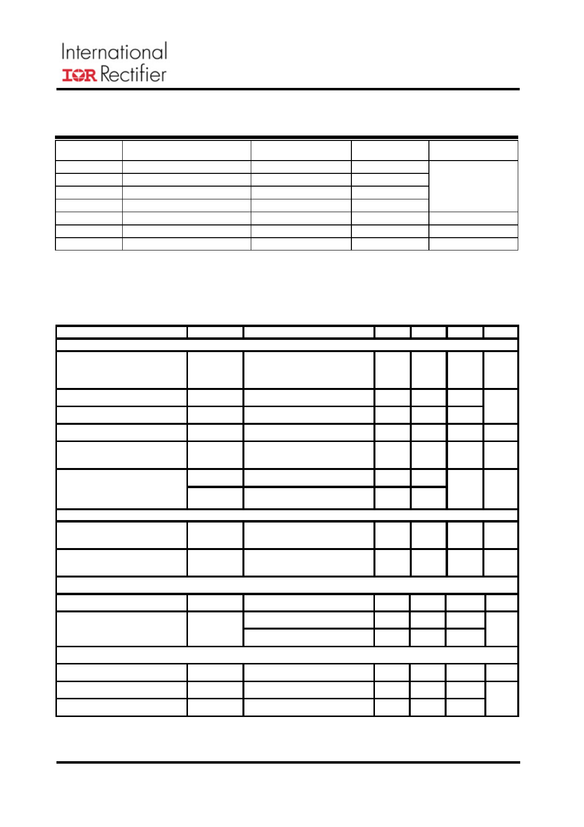
ABSOLUTE MAXIMUM RATINGS
(Voltages referenced to GND unless otherwise specified)
•
Vin ……………………………………………………. -0.3V to 25V
•
Vcc ……………….….…………….……..……….…… -0.3V to 8V (Note2)
•
Boot ……………………………………..……….…. -0.3V to 33V
•
SW …………………………………………..……… -0.3V to 25V(DC), -4V to 25V(AC, 100ns)
•
Boot to SW ……..…………………………….…..….. -0.3V to Vcc+0.3V (Note1)
•
OCSet ………………………………………….……. -0.3V to 30V (Max 30mA)
•
Input / output Pins ……………………………….. ... -0.3V to Vcc+0.3V (Note1)
•
PGND to GND ……………...………………………….. -0.3V to +0.3V
•
Storage Temperature Range ................................... -55°C To 150°C
•
Junction Temperature Range ................................... -40°C To 150°C (Note2)
•
ESD Classification …………………………… ……… JEDEC Class 1C
•
Moisture sensitivity level………………...………………JEDEC Level 3@260 °C (Note5)
Stresses beyond those listed under “Absolute Maximum Ratings” may cause permanent damage to the
device. These are stress ratings only and functional operation of the device at these or any other
conditions beyond those indicated in the operational sections of the specifications are not implied.
Note1:
Must not exceed 8V
Note2:
Vcc must not exceed 7.5V for Junction Temperature between -10
o
C and -40
o
C
W
/
C
W
/
C
W
/
C
o
PCB
J
*
o
JA
*
o
JA
)
FET
_
Ctrl
(
)
FET
_
Sync
(
2
45
45
=
=
=
-
θ
θ
θ
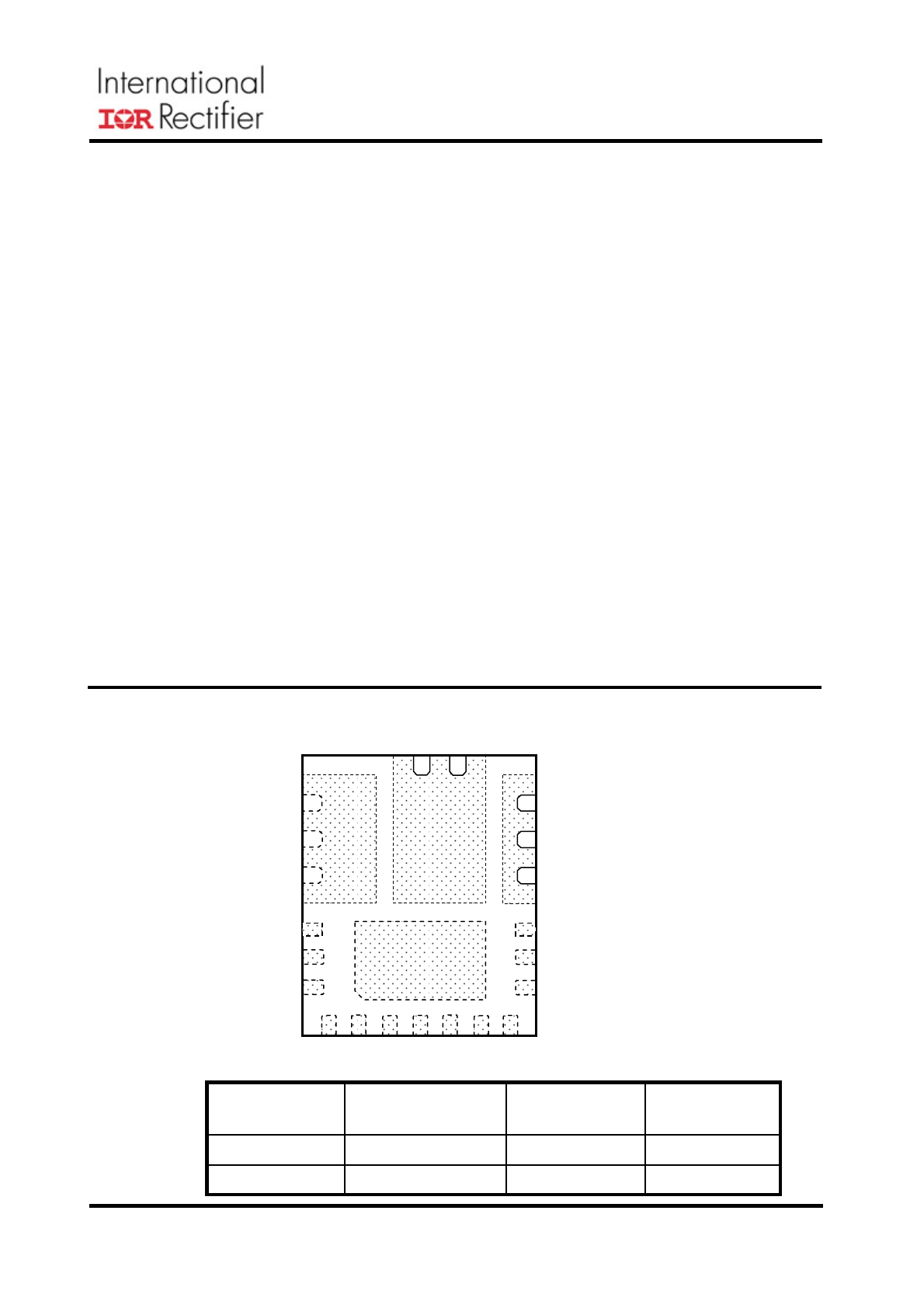
PACKAGE INFORMATION
4mm x 5mm POWER QFN
4000
17
IR3856MTRPbF
M
750
PARTS PER
REEL
17
PIN COUNT
IR3856MTR1PbF
PACKAGE
DESCRIPTION
M
PACKAGE
DESIGNATOR
ORDERING INFORMATION
13
V
IN
12
SW
11
PGnd
17
Gnd
1
2
3
4
5
6
7
8
9
16
15
Fb Vsns COMP Gnd Rt SS OCSet
PGood
Enable
Boot
Seq
Vcc
10
14
Sync
*
Exposed pads on underside
are connected to copper
pads of a 4-layer (2 oz.) PCB
Rev 4.0
3
PD-97528
IR3856MPbF
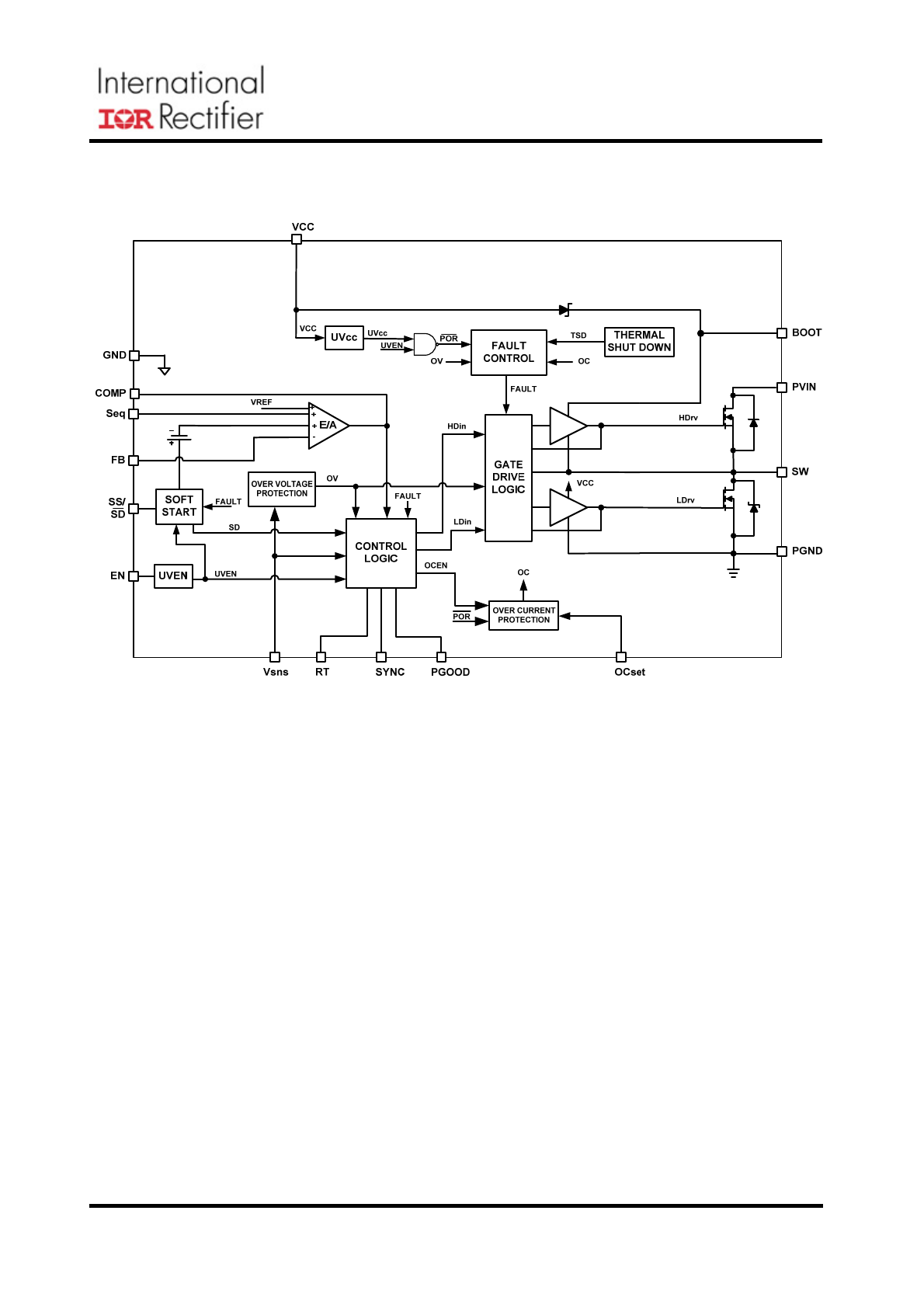
Block Diagram
Fig. 2. Simplified block diagram of the IR3856
Rev 4.0
4
PD-97528
IR3856MPbF
Pin Description
Pin
Name
Description
1
Fb
Inverting input to the error amplifier. This pin is connected directly to the
output of the regulator via resistor divider to set the output voltage and
provide feedback to the error amplifier.
2
Vsns
Sense pin for PGood
3
Comp
Output of error amplifier. An external resistor and capacitor network is
typically connected from this pin to Fb pin to provide loop compensation.
4;17
Gnd
Signal ground for internal reference and control circuitry.
5
Rt
Set the switching frequency. Connect an external resistor from this pin to
Gnd to set the switching frequency. See Table 1 for Fs vs. Rt.
6
SS/SD
Soft start / shutdown. This pin provides user programmable soft-start
function. Connect an external capacitor from this pin to Gnd to set the
start up time of the output voltage. The converter can be shutdown by
pulling this pin below 0.3V.
7
OCSet
Current limit set point. A resistor from this pin to SW pin will set the
current limit threshold.
8 PGood
Power Good status pin. Output is open drain. Connect a pull up resistor
from this pin to Vcc.
9
Sync
Sync pin, connect external system clock to synchronize multiple POLs
with the same frequency
10 V
CC
This pin powers the internal IC and the drivers. A minimum of 1uF high
frequency capacitor must be connected from this pin to the power ground
(PGnd).
11
PGnd
Power Ground. This pin serves as a separated ground for the MOSFET
drivers and should be connected to the system’s power ground plane.
12 SW
Switch node. This pin is connected to the output inductor.
13 V
IN
Input voltage connection pin.
14
Boot
Supply voltage for high side driver. A 0.1uF capacitor must be connected
from this pin to SW.
15
Enable
Enable pin to turn on and off the device. Use two external resistors to set
the turn on threshold (see Enable section). Connect this pin to Vcc if it is
not used.
16
Seq
Sequence pin. Use two external resistors to set Simultaneous Power up
sequencing. If this pin is not used connect to Vcc.
Rev 4.0
5
PD-97528
IR3856MPbF
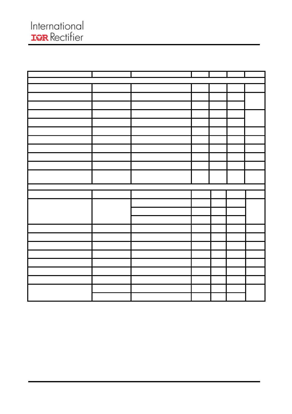
Recommended Operating Conditions
* Note: SW node should not exceed 25V
Electrical Specifications
Unless otherwise specified, these specification apply over 4.5V< V
cc
<5.5V, V
in
=12V, 0
o
C<T
j
< 125
o
C.
Typical values are specified at T
a
= 25
o
C.
Symbol Definition
Min
Max Units
V
in
Input
Voltage
1.5
21*
V
cc
Supply
Voltage
4.5
5.5
Boot to SW
Supply Voltage
4.5
5.5
V
o
Output
Voltage
0.7 0.9*Vin
V
I
o
Output
Current
0
6
A
Fs Switching
Frequency
225
1650 kHz
T
j
Junction
Temperature -40
125
o
C
PARAMETER SYMBOL
TEST
CONDITION
MIN
TYP
MAX
UNIT
POWER STAGE
Power Losses
P
loss
Vcc=5V,
V
in
=12V, V
o
=1.8V,
I
o
=6A, Fs=600kHz, L=1.0uH,
Note4
1.11 W
Top Switch
R
ds(on)_Top
V
Boot
-V
sw
=5V, I
D
=6A, Tj=25
o
C
22
29
Bottom Switch
R
ds(on)_Bot
V
cc
=5V, I
D
=6A, T
j
=25
o
C
13.4 19
m
Ω
Deadband Time
T
db
Note4
5 10 30 ns
Bootstrap Diode Forward
Voltage
I(Boot)=
30mA
180 260 470 mV
Isw SW=0V,
Enable=0V
SW leakage Current
SW=0V,
Enable=high,
SS=3V,
Vseq=0V, Note4
6
uA
SUPPLY CURRENT
V
CC
Supply Current (Standby)
I
CC(Standby)
SS=0V, Vcc=5V, Enable low ,
No Switching
500
uA
V
CC
Supply Current (Dyn)
I
CC(Dyn)
SS=3V, Vcc=5V, Enable high,
Fs=500kHz
9.25 mA
REFERENCE VOLTAGE
Feedback Voltage
VFB
0.7
V
0
o
C<Tj<125
o
C -1.0
+1.0
Accuracy
-40
o
C<Tj<125
o
C, Note3
-2.0
-2.0
%
SOFT START / SD
Soft Start Current
ISS
Source
14
20
26
uA
Soft Start Clamp Voltage
Vss(clamp)
2.7
3.0
3.3
Shutdown Output Threshold
SD
0.3
V
Rev 4.0
6
PD-97528
IR3856MPbF
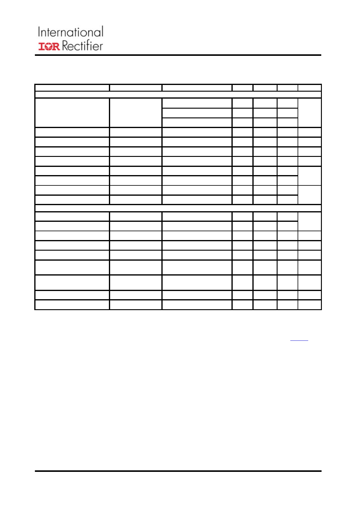
Electrical Specifications (continued)
Unless otherwise specified, these specifications apply over 4.5V< V
cc
<5.5V, V
in
=12V, 0
o
C<T
j
< 125
o
C.
Typical values are specified at T
a
= 25
o
C.
PARAMETER SYMBOL
TEST
CONDITION
MIN
TYP
MAX
UNIT
ERROR AMPLIFIER
Input Offset Voltage
Vos
Vfb-Vseq, Vseq=0.8V
-10
+10
mV
Input Bias Current
IFb(E/A)
-1
+1
Input Bias Current
IVseq(E/A)
-1
+1
μA
Sink Current
Isink(E/A)
0.40
0.85
1.2
Source Current
Isource(E/A)
8
10
13
mA
Slew Rate
SR
Note4
7 12 20 V/
μs
Gain-Bandwidth Product
GBWP
Note4
20 30 40 MHz
DC Gain
Gain
Note4
100 110 120 dB
Maximum Voltage
Vmax(E/A)
Vcc=4.5V
3.4
3.5
3.75
V
Minimum Voltage
Vmin(E/A)
120
220
mV
Seq Common Mode Voltage
Note4
0 1 V
OSCILLATOR
Rt
Voltage
Vrt
0.665 0.7 0.735 V
Rt=59K 225
250
275
Rt=28.7K 450
500
550
Frequency Range
F
S
Rt=9.31K, Note4
1350
1500
1650
kHz
Ramp Amplitude
Vramp
Note4
1.8 Vp-p
Ramp Offset
Ramp(os)
Note4
0.6 V
Min Pulse Width
Dmin(ctrl)
Note4
50 ns
Max Duty Cycle
Dmax
Fs=250kHz
92
%
Fixed Off Time
Toff
Note4
130
200 ns
Sync Frequency Range
Fsync
225
1650
kHz
Sync Pulse Duration
Tsync
100
200
ns
High
2
Sync Level Threshold
Low
0.6
V
Rev 4.0
7
PD-97528
IR3856MPbF
PARAMETER SYMBOL
TEST
CONDITION
MIN
TYP
MAX
UNIT
FAULT PROTECTION
Fs=250kHz
20.8 23.6 26.4
Fs=500kHz 43
48.8
54.6
OCSET Current
I
OCSET
Fs=1500kHz 136
154
172
uA
OC comp Offset Voltage
V
OFFSET
Note4
-10 0 +10
mV
SS
off
time
SS_Hiccup
4096
Cycles
OVP Trip Threshold
OVP(trip)
Vsns Rising
110
115
120
%Vref
OVP Fault Prop. Delay
OVP(delay)
Note4
150
ns
Therm al Shutdown
Note4
140
Therm al Hysteresis
Note4
20
°C
V
CC
-Start-Threshold V
CC
_UVLO_Start
Vcc Rising Trip Level
3.95
4.15
4.35
V
CC
-Stop-Threshold V
CC
_UVLO_Stop
Vcc Falling Trip Level
3.65
3.85
4.05
V
INPUT/OUTPUT SIGNAL
Enable-Start-Threshold Enable_UVLO_Start
Supply
ramping
up
1.14 1.2 1.36
Enable-Stop-Threshold Enable_UVLO_Stop
Supply
ramping
down
0.9
1.0
1.06
V
Enable leakage current
Ien
Enable=3.3V
15
uA
Power Good Threshold
VPG
Vsns Rising
80
85
90
%Vref
PGood Comparator Delay
PG(Delay)
Vsns Rising
256/Fs
s
PGood Delay Comparator
Threshold
SS(Delay)
Relative to charge voltage,
SS rising
2 2.1
2.3 V
PGood Delay Comparator
Hysteresis
Delay(SShys)
Note4
260 300 340 mV
PGood
Leakage
Current
I(PGDlk)
0 10 uA
PGood Voltage Low
PG(voltage)
I
Pgood
=-5mA
0.5
V
Note3: Cold temperature performance is guaranteed via correlation using statistical quality control. Not tested in production.
Note4: Guaranteed by Design but not tested in production.
Note5: Upgrade to industrial/MSL2 level applies from date codes 1227 (marking explained on application note
AN1132
page 2).
Products with prior date code of 1227 are qualified with MSL3 for Consumer market.
Electrical Specifications (continued)
Unless otherwise specified, these specification apply over 4.5V< V
cc
<5.5V, V
in
=12V, 0
o
C<T
j
< 125
o
C.
Typical values are specified at T
a
= 25
o
C.
Rev 4.0
8
PD-97528
IR3856MPbF
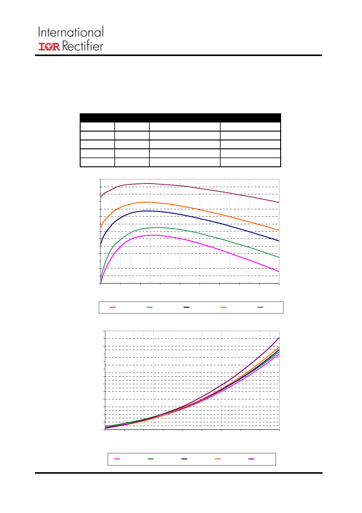
Typical Efficiency and Power Loss Curves
Vin=12V, Vcc=5V, Io=0.6A- 6A, F
s
=600kHz, Room Temperature, No Air Flow
The table below shows the inductors used for each of the output voltages
in the efficiency measurement.
79
81
83
85
87
89
91
93
95
97
0.6
1.2
1.8
2.4
3.0
3.6
4.2
4.8
5.4
6.0
Load Current (A)
Eff
iciency (%)
1.0V
1.2V
1.5V
1.8V
3.3V
5V
0.10
0.30
0.50
0.70
0.90
1.10
1.30
1.50
0.6
1.2
1.8
2.4
3.0
3.6
4.2
4.8
5.4
6.0
Load Current (A)
Pow
e
r Loss (
W
)
1.0V
1.2V
1.5V
1.8V
3.3V
5.0V
Vo (V)
L (uH)
P/N
DCR (mOhm)
1
0.68
PCMB065T-0R68
3.9
1.2
0.82
SPM6550T-0R82M
4.2
1.5
1.0
SPM6550T-1R0M
4.7
1.8
1.0
SPM6550T-1R0M
4.7
3.3
3.3
7443340220
4.4
5
3.3
7443340220
4.4
Rev 4.0
9
PD-97528
IR3856MPbF
Typical Efficiency and Power Loss Curves
Vin=5V, Vcc=5V, Io=0.6A- 6A, Fs=600kHz, Room Temperature, No Air Flow
The table below shows the inductors used for each of the output voltages
in the efficiency measurement.
83
84
85
86
87
88
89
90
91
92
93
94
95
96
97
0.6
1.2
1.8
2.4
3.0
3.6
4.2
4.8
5.4
6.0
Load Current (A)
Ef
ficiency (%)
1.0V
1.2V
1.5V
1.8V
3.3V
0.10
0.20
0.30
0.40
0.50
0.60
0.70
0.80
0.90
1.00
1.10
1.20
1.30
1.40
0.6
1.2
1.8
2.4
3.0
3.6
4.2
4.8
5.4
6.0
Load Current (A)
P
o
wer Loss (W)
1.0Vout
1.2Vout
1.5Vout
1.8Vout
3.3Vout
Vo (V)
L (uH) P/N
DCR (mOhm)
1
0.68
PCMB065T-0R68
3.9
1.2
0.68
PCMB065T-0R68
3.9
1.5
0.82
SPM6550T-0R82M
4.2
1.8
1.00
SPM6550T-1R0M
4.7
3.3
1.00
SPM6550T-1R0M
4.7
Rev 4.0
10
PD-97528
IR3856MPbF
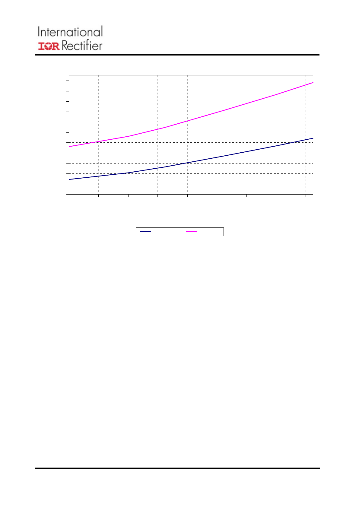
8
10
12
14
16
18
20
22
24
26
28
30
-40
-20
0
20
40
60
80
100
120
Temperature [ °C]
Resist
an
ce [
m
Ω
]
Sync-FET
Ctrl-FET
Rdson of MOSFETs Over Temperature at Vcc=5V