
IR3827
1
www.irf.com
© 2013 International Rectifier
July 18, 2013
6A Highly Integrated SupIRBuck
TM
Single-
Input Voltage, Synchronous Buck Regulator
FEATURES
DESCRIPTION
• Single input voltage range from 5V to 21V
• Wide input voltage range from 1.0V to 21V with
external V
CC
bias voltage
• Output voltage range from 0.6V to 0.86% PVin
• Enhanced line/load regulation with feedforward
• Programmable switching frequency up to
1.2MHz
• Three user selectable soft-start time
• User selectable LDO output voltage
• Enable input with voltage monitoring capability
• Thermally compensated current limit with robust
hiccup mode over current protection
• Synchronization to an external clock
• Enhanced Pre-bias start-up
• Precise reference voltage (0.6V+/-0.6%)
• Open-drain PGood indication
• Optional power up sequencing
• Integrated MOSFET drivers and bootstrap diode
• Thermal Shut Down
• Monotonic Start-Up
• Operating temp: -40°C < T
j
< 125°C
• Package size: 4mm x 5mm PQFN
• Lead-free, Halogen-free and RoHS6 Compliant
The IR3827 SupIRBuck
TM
is an easy-to-use, fully
integrated and highly efficient DC/DC regulator.
The onboard PWM controller and MOSFETs make
IR3827 a space-efficient solution, providing accurate
power delivery for low output voltage applications.
IR3827 is a versatile regulator which offers
programmable switching frequency and internally set
current limit while operating in wide range of input and
output voltage conditions.
The switching frequency is programmable from 300kHz
to 1.2MHz for an optimum solution. It also features
important protection functions, such as Pre-Bias
startup, thermally compensated current limit, over
voltage protection and thermal shutdown to give
required system level security in the event of fault
conditions.
APPLICATIONS
• Computing Applications
• Set Top Box Applications
• Storage Applications
• Data Center Applications
• Distributed Point of Load Power Architectures
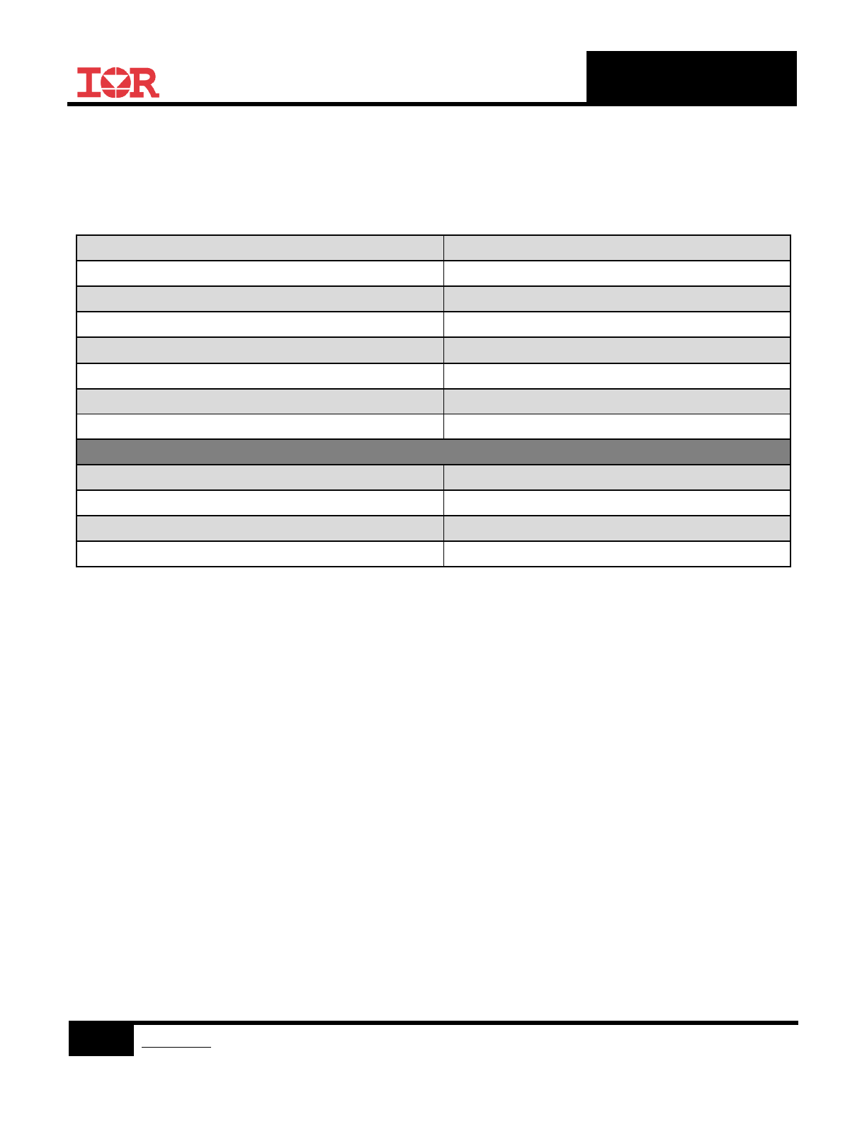
ORDERING INFORMATION
Base Part Number
Package Type
Standard Pack
Orderable Part Number
Form
Quantity
IR3827
PQFN 4 mm x 5 mm
Tape and Reel
750
IR3827MTR1PBF
IR3827
PQFN 4 mm x 5 mm
Tape and Reel
4000
IR3827MTRPBF
IR3827
PBF – Lead Free
TR/TR1 – Tape and Reel
M – PQFN Package
IR3827
2
www.irf.com
© 2013 International Rectifier
July 18, 2013
BASIC APPLICATION
Boot
Vcc/
LDO_out
Fb
Comp
Gnd PGnd
SW
PGood
Rt/Sync
PVin
Vin
Enable
IR3827
SS_Select
Vin
PGood
Vo
LDO_Select
Seq
Figure 1 IR3827 Basic Application Circuit Figure 2 IR3827 Efficiency
PINOUT DIAGRAM
IR3827
13
12
11
17
14
15
16
1
2
3
4
5
6
8
9
10
Fb
SS
_Se
lect
Comp
Gnd
Rt
/Sync
PGood
LDO_Select
Vin
Vcc/LDO_Out
PGnd
PVin
Boot
Enable
SW
GND
Seq
7
N/
C
Figure 3 4mm x 5mm PQFN (Top View)
IR3827
3
www.irf.com
© 2013 International Rectifier
July 18, 2013
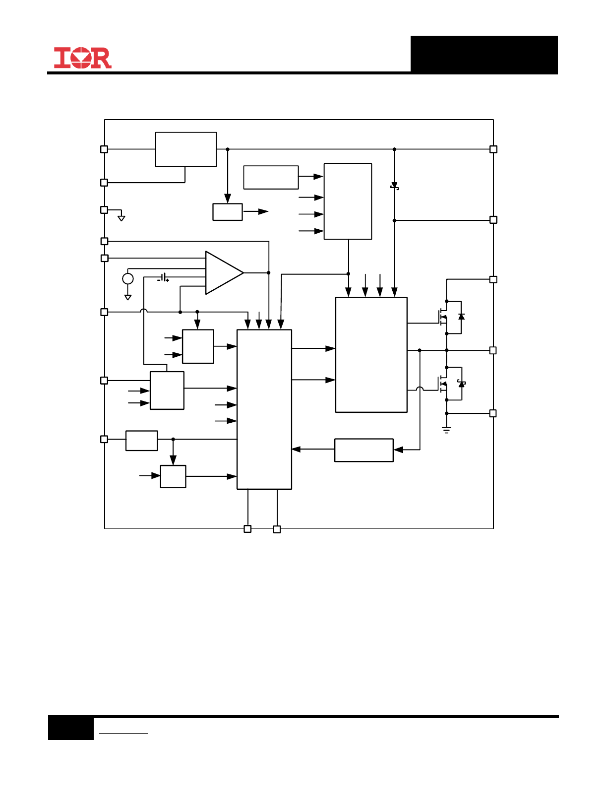
BLOCK DIAGRAM
Seq
Fb
Rt/Sync
SW
PGnd
Enable
VCC
OC
TSD
HDin
UVcc
UVEN
HDrv
LDrv
Vin
SSOK
0.6V
VREF
SEQ
POR
POR
UVcc
Gnd
OC
OV
OV
Vin
SS_Select
Fb
LDO_Select
Vcc/ LDO_Out
5.1V/6.9V
Internal LDO
UVcc
THERMAL
SHUT DOWN
FAULT
CONTROL
+
-
+
+
E/A
Comp
VREF
+
-
CONTROL
LOGIC
0.15V
SOFT
START
UVEN
POR
OVER
VOLTAGE
FAULT
POR
VREF
INTL_SS
POR
GATE
DRIVE
PVin
LDin
Boot
VCC
POR
FAULT
Over Current
Protection
PGood
Figure 4 Simplified Block Diagram
IR3827
4
www.irf.com
© 2013 International Rectifier
July 18, 2013
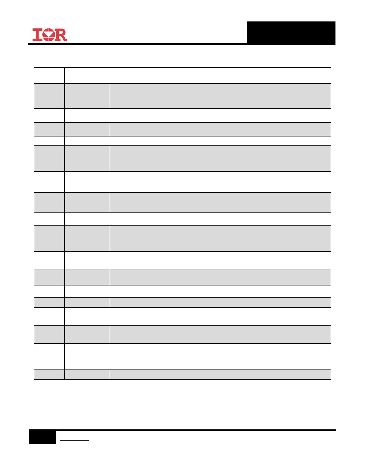
PIN DESCRIPTIONS
PIN #
PIN NAME
PIN DESCRIPTION
1
Fb
Inverting input to the error amplifier. This pin is connected directly to the output of the
regulator via a resistor divider to set the output voltage and to provide the feedback signal
to the error amplifier.
2
N/C
Should not be connected to other signals on PCB layout. It is internally connected for
testing purpose.
3
Comp
Output of error amplifier. An external resistor and capacitor network is typically connected
from this pin to Fb pin to form a loop compensator.
4, 17
Gnd
Signal ground for internal reference and control circuitry.
5
Rt/Sync
Multi-function pin to set the switching frequency. The internal oscillator frequency is set
with a resistor between this pin and Gnd. Or synchronization to an external clock by
connecting this pin to the external clock signal through a diode.
6
SS_Select
Soft start selection pin. Three user selectable soft start time is available: 1.5ms
(SS_Select=Vcc), 3ms (SS_Select=Float), 6ms (SS_Select=Gnd)
7
PGood
Open-drain power good indication pin. Connect a pull-up resistor from this pin to Vcc.
8
LDO_Select
LDO output voltage selection pin. Float gives 5.1V and low 0V (Gnd) gives 6.9V
9
V
in
Input for internal LDO. A 1.0µF capacitor should be connected between this pin and
PGnd. If external supply is connected to Vcc/LDO_out pin, this pin should be shorted to
Vcc/LDO_out pin. Connecting this pin to PV
in
can also implement the input voltage
feedforward.
10
Vcc/LDO_Out
Output of the internal LDO and optional input of an external biased supply voltage. A
minimum 2.2µF ceramic capacitor is recommended between this pin and PGnd.
11
PGnd
Power Ground. This pin serves as a separated ground for the MOSFET drivers and
should be connected to the system’s power ground plane.
12
SW
Switch node. Connected this pin to the output inductor.
13
PV
in
Input voltage for power stage.
14
Boot
Supply voltage for high side driver, a 100nF capacitor should be connected between this
pin and SW pin.
15
Enable
Enable pin to turn on and off the device. Input voltage monitoring (input UVLO) can also
be implemented by connecting this pin to PVin pin through a resistor divider.
16
Seq
Sequence pin to do simultaneous and ratiometric sequencing operation. A resistor divider
can be connected from master output to this pin for sequencing mode of operation. If not
used, leave it open.
17
Gnd
Signal ground for internal reference and control circuitry.
IR3827
5
www.irf.com
© 2013 International Rectifier
July 18, 2013
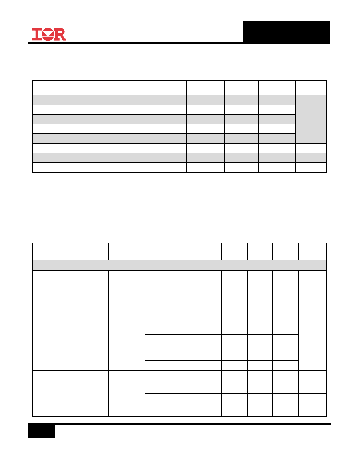
ABSOLUTE MAXIMUM RATINGS
Stresses beyond these listed under “Absolute Maximum Ratings” may cause permanent damage to the device.
These are stress ratings only and functional operation of the device at these or any other conditions beyond those
indicated in the operational sections of the specifications are not implied.
PVin, Vin to PGnd (Note 4)
-0.3V to 25V
Vcc/LDO_Out to PGnd (Note 4)
-0.3V to 8V (Note 1)
Boot to PGnd (Note 4)
-0.3V to 33V
SW to PGnd (Note 4)
-0.3V to 25V (DC), -4V to 25V (AC, 100ns)
Boot to SW
-0.3V to V
CC
+ 0.3V (Note 2)
PGood, SS_Select to Gnd (Note 4)
-0.3V to V
CC
+ 0.3V (Note 2)
Other Input/Output Pins to Gnd (Note 4)
-0.3V to +3.9V
PGnd to Gnd
-0.3V to +0.3V
THERMAL INFORMATION
Junction to Ambient Thermal Resistance
Ɵ
jA
32 °C/W (Note 3)
Junction to PCB Thermal Resistance Ɵ
j-PCB
2 °C/W
Storage Temperature Range
-55°C to 150°C
Junction Temperature Range
-40°C to 150°C
Note 1: Vcc must not exceed 7.5V for Junction Temperature between -10°C and -40°C
Note 2: Must not exceed 8V
Note 3: Based on IRDC3827 demo board - 2.6”x2.2”, 4-layer PCB board using 2 oz. copper on each layer.
Note 4: PGnd pin and Gnd pin are connected together.
IR3827
6
www.irf.com
© 2013 International Rectifier
July 18, 2013
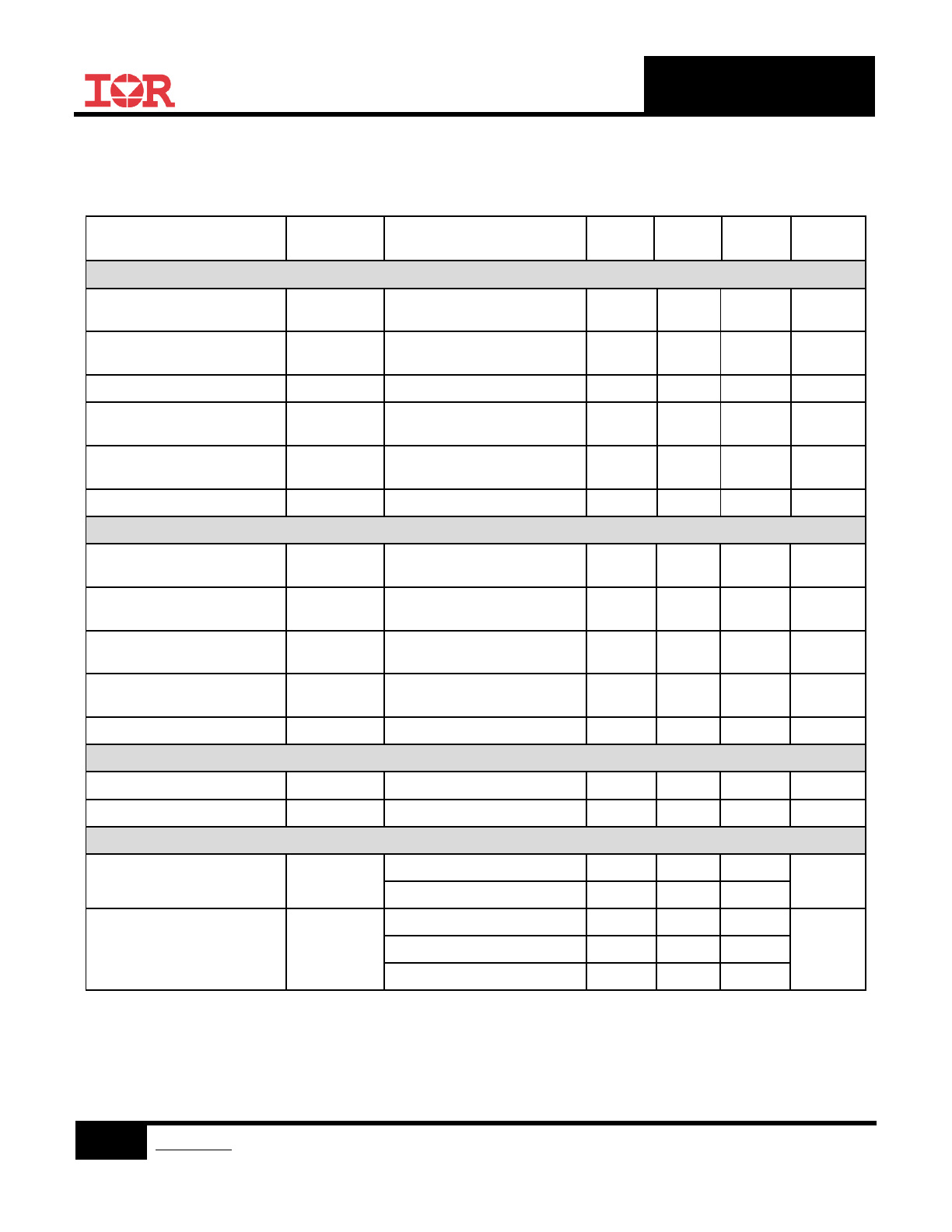
ELECTRICAL SPECIFICATIONS
RECOMMENDED OPERATING CONDITIONS
SYMBOL
MIN
MAX
UNITS
Input Voltage Range with External Vcc Note 5, Note 7
PV
in
1.0
21
V
Input Voltage Range with Internal LDO Note 6, Note 7
V
in
, PV
in
5.5
21
Supply Voltage Range (Note 6)
V
CC
4.5
7.5
Supply Voltage Range (Note 6)
Boot to SW
4.5
7.5
Output Voltage Range
V
0
0.6
0.86 x PV
in
Output Current Range
I
0
0
6
A
Switching Frequency
F
S
300
1200
kHz
Operating Junction Temperature
T
J
-40
125
°C
Note 5: V
in
is connected to V
cc
to bypass the internal LDO.
Note 6: V
in
is connected to PV
in
. For single-rail applications with PV
in
=V
in
= 4.5V-5.5V, please refer to the application information in the
section of User Selectable Internal LDO and the section of Over Current Protection.
Note 7: Maximum SW node voltage should not exceed 25V.
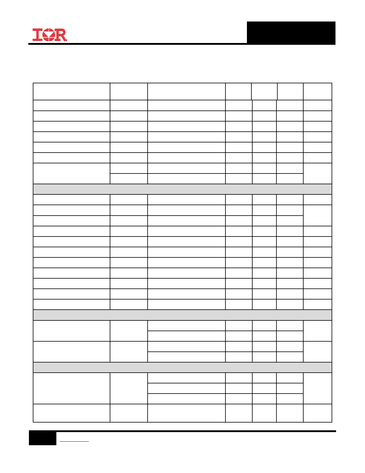
ELECTRICAL CHARACTERISTICS
Unless otherwise specified, these specifications apply over, 5.5V < V
in
= PV
in
< 21V, 0°C < T
J
< 125°C, LDO_Select=Gnd,
SS_Select=Float. Typical values are specified at T
a
= 25°C.
PARAMETER
SYMBOL
CONDITIONS
MIN
TYP
MAX
UNITS
Power Stage
Power Losses
P
LOSS
PV
in
=V
in
= 12V, V
o
=1.2V,
I
o
= 6A, F
s
=600kHz,L=1.0uH,
LDO_Select=Gnd. Note 8
1.1
W
PV
in
=V
in
=12V, V
o
=1.2V,
I
o
=6A, F
s
=600kHz, L=1.0uH,
LDO_Select=Float. Note 8
1.3
Top Switch R
DS(ON)
R
DS(on)-T
V
BOOT
-Vsw=5.1V,I
o
= 6A,
T
j
= 25°C
21
29
mΩ
V
BOOT
-Vsw=6.9V,I
o
= 6A,
T
j
= 25°C
16
22
Bottom Switch R
DS(ON)
R
DS(on)-B
V
cc
= 5.1V, I
o
= 6A, T
j
= 25°C
21.4
30
V
cc
= 6.9V, I
o
= 6A, T
j
= 25°C
16.8
23
Bootstrap Diode Forward
Voltage
V
D
I(Boot) = 10mA
180
260
470
mV
SW Leakage Current
V
SW
= 0V, Enable = 0V
1
µA
V
SW
= 0V, Enable = High,
V
SEQ
=0V
1
µA
Dead Band Time
T
D
Note 8
10
ns
IR3827
7
www.irf.com
© 2013 International Rectifier
July 18, 2013
ELECTRICAL CHARACTERISTICS (CONTINUED)
Unless otherwise specified, these specifications apply over, 5.5V < V
in
= PV
in
< 21V, 0°C < T
J
< 125°C, LDO_Select=Gnd,
SS_Select=Float. Typical values are specified at T
a
= 25°C.
PARAMETER
SYMBOL
CONDITIONS
MIN
TYP
MAX
UNITS
Supply Current
Vin Supply Current (standby)
I
in(Standby)
EN = Low, No Switching
200
µA
Vin Supply Current
(dynamic)
I
in(Dyn)
EN = High, F
s
= 600kHz,
V
in
= PV
in
= 21V,
LDO_Select=Gnd
10
13
mA
EN = High, F
s
= 600kHz,
V
in
= PV
in
= 21V,
LDO_Select=Float
8
11
V
CC
/LDO_Out
Output Voltage
V
cc
V
in(min)
= 5.5V, I
o
= 0-30mA,
Cload =2.2uF,
LDO_Select=Float
4.75
5.1
5.4
V
V
in(min)
= 7.3V, I
o
= 0-30mA,
Cload = 2.2uF,
LDO_Select=Gnd
6.5
6.9
7.2
LDO_Select Input bias
Current
LDO_Select=Gnd
30
60
uA
LDO Dropout Voltage
V
cc_drop
V
in
=6.5V,I
o
=30mA,
Cload=2.2uF,
LDO_Select=Gnd
0.7
V
V
in
=4.7V,Io=25mA,
Cload=2.2uF,
LDO_Select=Float
0.7
Short Circuit Current
I
short
LDO_Select=Gnd
70
mA
Oscillator
Rt Voltage
V
Rt
1.0
V
Frequency Range
F
s
Rt = 80.6k
Ω
270
300
330
kHz
Rt = 39.2k
Ω
540
600
660
Rt = 19.1k
Ω
1080
1200
1320
Ramp Amplitude
V
ramp
V
in
= 7.3V, Vin slew rate max
= 1V/µs, Note 8
1.095
V
p-p
V
in
= 12V, Vin slew rate max
= 1V/µs, Note 8
1.80
V
in
= 21V, Vin slew rate max
= 1V/µs, Note 8
3.15
V
in
=V
cc
=5V, For external V
cc
operation, Note 8
0.75
IR3827
8
www.irf.com
© 2013 International Rectifier
July 18, 2013
ELECTRICAL CHARACTERISTICS (CONTINUED)
Unless otherwise specified, these specifications apply over, 5.5V < V
in
= PV
in
< 21V, 0°C < T
J
< 125°C, LDO_Select=Gnd,
SS_Select=Float. Typical values are specified at T
a
= 25°C.
PARAMETER
SYMBOL
CONDITIONS
MIN
TYP
MAX
UNITS
Ramp Offset
Note 8
0.16
V
Minimum Pulse Width
T
min(ctrl)
Note 8
60
ns
Maximum Duty Cycle
D
max
F
s
= 300kHz, V
in
=PV
in
= 12V
86
%
Fixed Off Time
T
off
Note 8
200
250
ns
Sync Frequency Range
F
sync
270
1320
kHz
Sync Pulse Duration
T
sync
100
200
ns
Sync Level Threshold
High
3
V
Low
0.6
Error Amplifier
Input Offset Voltage
V
FB
– V
SEQ
, V
SEQ
=0.3V
-3
+3
%
Input Bias Current (V
FB
)
I
FB
(E/A)
-1
+1
µA
Input Bias Current (V
SEQ
)
I
SEQ
(E/A)
0
+4
Sink Current
I
sink
(E/A)
0.4
0.85
1.2
mA
Source Current
I
source
(E/A)
4
7.5
11
mA
Slew Rate
SR
Note 8
7
12
20
V/µs
Gain-Bandwidth Product
GBWP
Note 8
20
30
40
MHz
DC Gain
Gain
Note 8
100
110
120
dB
Maximum Output Voltage
V
max
(E/A)
1.7
2.0
2.3
V
Minimum Output Voltage
V
min
(E/A)
100
mV
Common Mode Input Voltage
0
1.2
V
Reference Voltage (V
REF
)
Feedback Voltage
V
FB
LDO_Select= Gnd
0.6
V
LDO_Select= Float
0.6
Accuracy
0°C < T
j
< 70°C
-0.6
+0.6
%
-40°C < T
j
< 125°C ; Note 9
-1.2
+1.2
Soft Start
Soft Start Ramp Rate
SS_Select=High
0.34
0.4
0.46
mV/µs
SS_Select=Float
0.17
0.2
0.23
SS_Select=Gnd
0.085
0.1
0.115
SS_Select Input Bias Current
LDO_Select=Gnd
SS_Select=Gnd
40
80
uA
IR3827
9
www.irf.com
© 2013 International Rectifier
July 18, 2013
ELECTRICAL CHARACTERISTICS (CONTINUED)
Unless otherwise specified, these specifications apply over, 5.5V < V
in
= PV
in
< 21V, 0°C < T
J
< 125°C, LDO_Select=Gnd,
SS_Select=Float. Typical values are specified at T
a
= 25°C.
PARAMETER
SYMBOL
CONDITIONS
MIN
TYP
MAX
UNITS
Power Good
Power Good Turn on
Threshold
VPG
(on)
V
FB
rising
85
90
95
% V
REF
Power Good Lower Turn off
Threshold
VPG
(lower)
V
FB
falling
80
85
90
% V
REF
Power Good Turn on Delay
TPG
(ON)_D
V
FB
rising, see VPG
(on)
2.56
ms
Power Good Upper Turn off
Threshold
VPG
(upper)
V
FB
rising
115
120
125
% V
REF
PGood Comparator Delay
V
FB
< VPG
(lower)
or
V
FB
> VPG
(upper)
1
2
3.5
µs
PGood Voltage Low
PG(voltage)
I
PGood
= -5mA
0.5
V
Under-Voltage Lockout
V
cc
-Start Threshold
V
CC
UVLO
Start
V
cc
rising trip Level
3.9
4.1
4.3
V
V
cc
-Stop Threshold
V
CC
UVLO
Stop
Vcc falling trip Level
3.6
3.8
4.0
V
Enable-Start-Threshold
Enable
UVLO Start
ramping up
1.14
1.2
1.26
V
Enable-Stop-Threshold
Enable
UVLO Stop
ramping down
0.95
1
1.05
Enable Leakage Current
I
EN_LK
Enable = 3.3V
1
µA
Over-Voltage Protection
OVP Trip Threshold
OVP_V
th
V
FB
rising
115
120
125
% V
REF
OVP Comparator Delay
T
OVP_D
1
2
3.5
µs
Over-Current Protection
Current Limit
I
LIMIT
T
j
= 25°C, LDO_Select=Float
6.2
7.3
8.5
A
T
j
= 25°C, LDO_Select=Gnd
7.9
9.3
10.8
Hiccup Blanking Time
T
BLK_Hiccup
SS_Select = Vcc, Note 8
10
ms
SS_Select = Float, Note 8
20
SS_Select = Gnd, Note 8
40
IR3827
10
www.irf.com
© 2013 International Rectifier
July 18, 2013
ELECTRICAL CHARACTERISTICS (CONTINUED)
Unless otherwise specified, these specifications apply over, 5.5V < V
in
= PV
in
< 21V, 0°C < T
J
< 125°C, LDO_Select=Gnd,
SS_Select=float. Typical values are specified at T
a
= 25°C.
PARAMETER
SYMBOL
CONDITIONS
MIN
TYP
MAX
UNITS
Upper Gate Driver
Source Resistance
V
BOOT
-V
SW
= 5.1V, Note 8
3
Ω
Sink Resistance
V
BOOT
-V
SW
= 5.1V, Note 8
4
Lower Gate Driver
Source Resistance
V
CC
= 5.1V, Note 8
2
Ω
Sink Resistance
V
CC
= 5.1V, Note 8
0.8
Over-Temperature Protection
Thermal Shutdown Threshold
Note 8
145
°C
Hysteresis
Note8
20
Note 8: Guaranteed by design, but not tested in production.
Note 9: Cold temperature performance is guaranteed via correlation using statistical quality control. Not tested in production.