
September 10, 2012 | FINAL DATASHEET
1
IR3558
45A Integrated PowIRstage®
FEATURES
Peak efficiency up to 94.0% at 1.2V
Integrated driver, control MOSFET, synchronous
MOSFET and Schottky diode
Input voltage (VIN) operating range of 4.5V to 15V
Separate LVCC and HVCC from 4.5V to 13.2V to
optimize converter efficiency
Output current capability of 45A DC
Switching frequency up to 1.0MHz
Programmable thermal flag threshold from 70°C to
150°C
5V VCC with under voltage lockout
Low quiescent current
Enable control
Selectable regular 3.3V tri-state PWM logic or IR
Active Tri-Level (ATL) PWM logic
PCB footprint compatible with most IR3551 pins
Efficient dual sided cooling
Small 5mm x 6mm x 0.9mm PQFN package
Lead free RoHS compliant package
APPLICATIONS
Voltage Regulators for CPUs, GPUs, and DDR
memory arrays
High current, low profile DC-DC converters
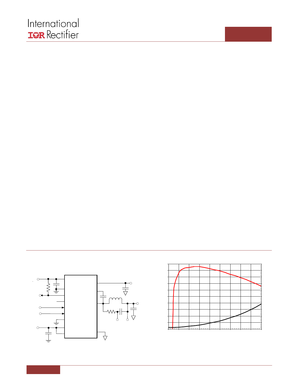
BASIC APPLICATION
SW
VIN
PGND
VCC
VCC
BOOST
VIN
VOUT
OTSET
5V
LGND
PWM
PWM
ENABLE
EN
4.5V to 15V
IR3558
OT#
OT#
CS+
CS-
HVCC
LVCC
MODE
PVCC
4.5V to 13.2V
Figure 1: IR3558 Basic Application Circuit
DESCRIPTION
The IR3558 integrated PowIRstage® is a synchronous buck
gate driver co-packed with a control MOSFET and a
synchronous MOSFET with integrated Schottky diode. It is
optimized internally for PCB layout, heat transfer and
driver/MOSFET timing. Custom designed gate driver and
MOSFET combination enables higher efficiency at lower
output voltages required by cutting edge CPU, GPU and
DDR memory designs.
Up to 1.0MHz switching frequency enables fast transient
response, allowing miniaturization of output inductors as
well as input and output capacitors while maintaining high
efficiency. The IR3558’s superior efficiency enables
smallest size and lower solution cost. The IR3558 PCB
footprint is compatible with most pins of the IR3551 (50A).
The IR3558 provides two selectable PWM logic modes, the
3.3V tri-state PWM logic or International Rectifier’s Active
Tri-Level
TM
(ATL) PWM logic. The ATL PWM logic eliminates
a dedicated Body-Braking® pin and improves the transient
response of the converter during load release.
The IR3558 provides a thermal flag output with
programmable threshold from 70°C to 150°C, which makes
it possible to adjust the thermal protection threshold
based on the PCB layout and thermal distribution.
The IR3558 is optimized specifically for CPU core power
delivery in server applications. The ability to meet the
stringent requirements of the server market also makes
the IR3558 ideally suited to powering GPU and DDR
memory designs and other high current applications.
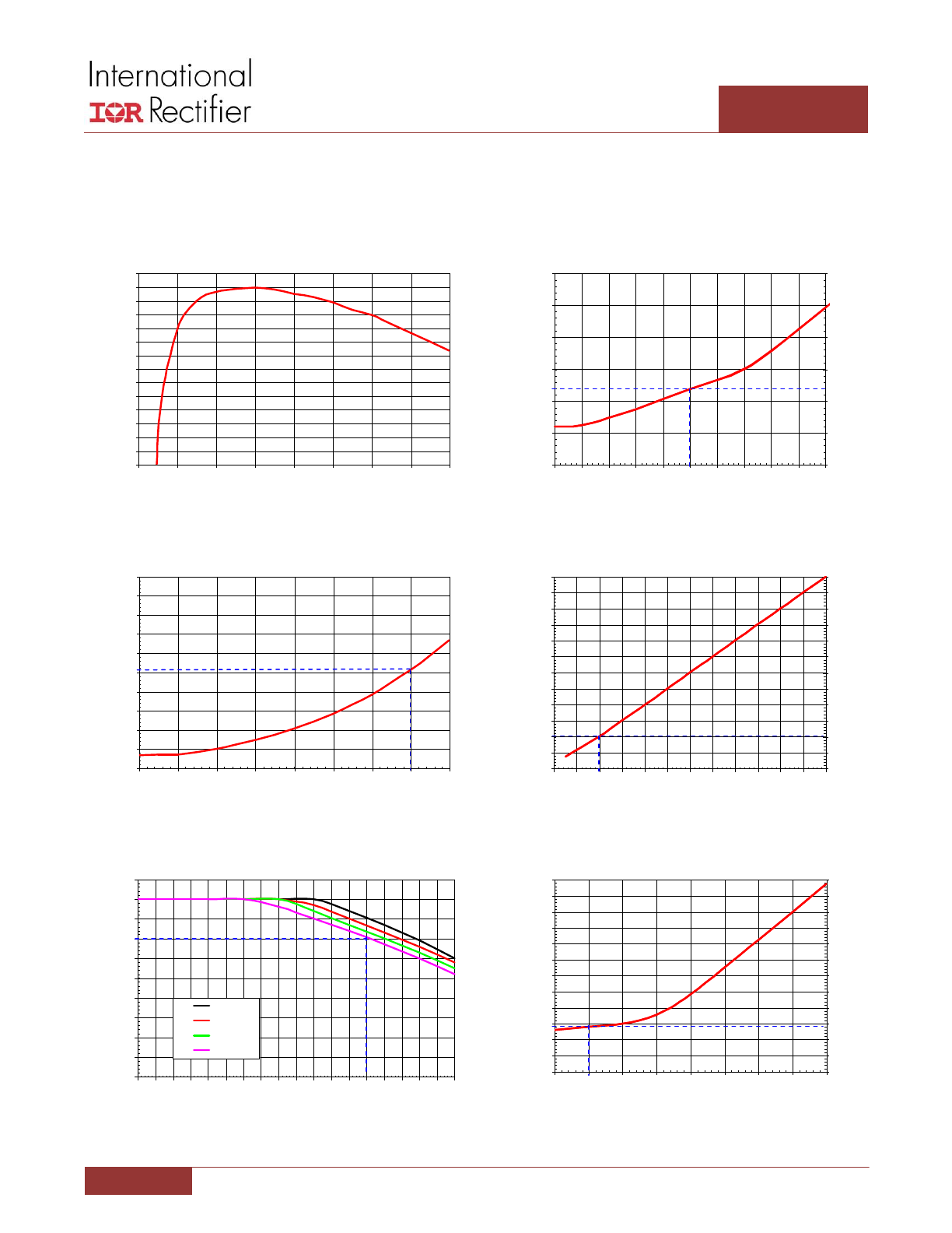
Figure 2: Typical IR3558 Efficiency & Power Loss
(See Note 2 on Page 7)
75
77
79
81
83
85
87
89
91
93
95
0
5
10
15
20
25
30
35
40
45
Output Current (A)
Ef
fi
ci
en
cy
(
%
)
0
2
4
6
8
10
12
14
16
18
20
P
o
w
er
L
o
ss
(
W
)
September 10, 2012 | FINAL DATASHEET
2
IR3558
45A Integrated PowIRstage®
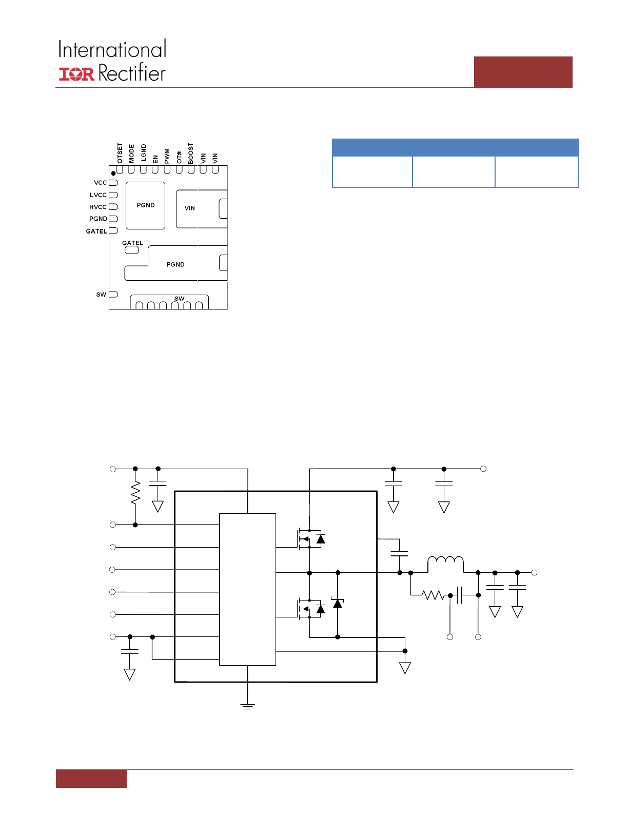
PINOUT DIAGRAM
Figure 3: IR3558 Pin Diagram, Top View
ORDERING INFORMATION
Package
Tape & Reel Qty
Part Number
PQFN, 28 Lead
5mm x 6mm
4000
IR3558MTRPBF
TYPICAL APPLICATION DIAGRAM
SW
PWM
VIN
PGND
Gate
Drivers
and
Over
Temperat-
ure
Detection
MODE
VCC
OT#
PVCC
VCC
BOOST
VIN
VOUT
PWM
LVCC
OT#
ENABLE
EN
OTSET
OTSET
LGND
IR3558
4.5V to 5.5V
4.5V to 15V
C2
10uF x 2
C5
0.22uF
C3
0.1uF
R1
10k
C6
0.22uF
R2
2.49k
L1
150nH
C8
470uF
1
16-19
20
21
22
23
26
25
2
24
14, 15
6-13
C1
0.1uF
PGND 4, 27
C7
22uF
MODE
HVCC
3
4.5V to 13.2V
CS+
CS-
C4
1uF
Figure 4: Application Circuit
September 10, 2012 | FINAL DATASHEET
3
IR3558
45A Integrated PowIRstage®
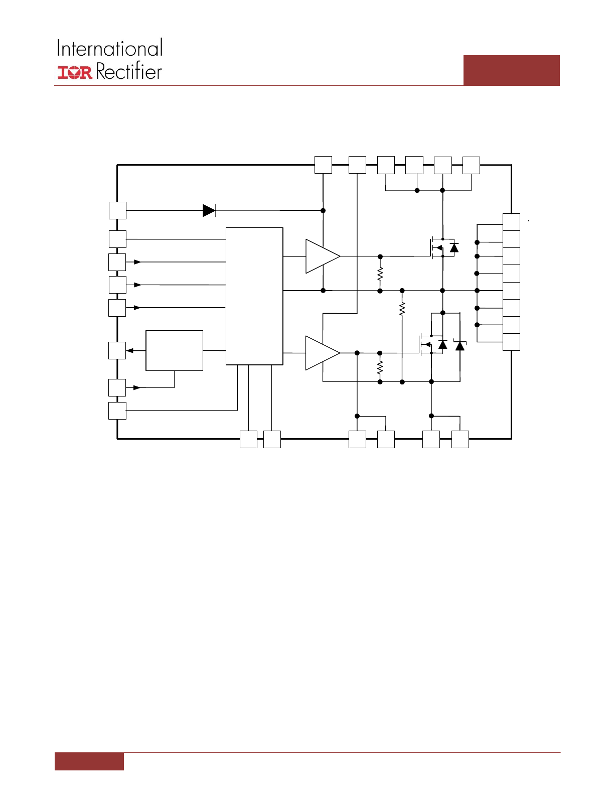
FUNCTIONAL BLOCK DIAGRAM
OT#
PWM
6
7
8
9
10
11
12
13
16
17
18
19
VIN
VIN
VIN
VIN
SW
SW
SW
SW
SW
SW
SW
SW
27
14
15
PGND
PGND
PGND
20
BOOST
Power-on
Reset
(POR),
PWM
Mode,
Reference,
and
Dead-time
Control
22
OTSET
26
LVCC
1
EN
23
5
28
GATEL
GATEL
Driver
Driver
21
24
LGND
25
MODE
Thermal
Detection
VCC
4
PGND
IR3558
3
HVCC
2
VCC
Figure 5: IR3558 Functional Block Diagram
September 10, 2012 | FINAL DATASHEET
4
IR3558
45A Integrated PowIRstage®
PIN DESCRIPTIONS
PIN #
PIN NAME
PIN DESCRIPTION
1
VCC
Bias voltage for control logic. Connect VCC to a 5V supply. Connect a minimum 0.1uF
capacitor between VCC and LGND.
2
LVCC
Supply voltage for the low-side driver. Connect LVCC to a 4.5V to 13.2V supply. Connect
a minimum 0.1uF capacitor between LVCC and PGND (pin 4).
3
HVCC
Supply voltage for the high-side driver. Connect HVCC to a 4.5V to 13.2V supply.
Connect a minimum 0.1uF capacitor between HVCC and PGND (pin 4).
4, 14, 15, 27
PGND
Power ground of low-side MOSFET driver and the synchronous MOSFET.
5, 28
GATEL
Low-side MOSFET driver pins that can be connected to a test point in order to observe
the waveform.
6 – 13
SW
Switch node of synchronous buck converter.
16 – 19
VIN
High current input voltage connection. Recommended operating range is 4.5V to 15V.
Connect at least two 10uF 1206 ceramic capacitors and a 0.1uF 0402 ceramic capacitor.
Place the capacitors as close as possible to VIN pins and PGND pins (14-15). The 0.1uF
0402 capacitor should be on the same side of the PCB as the IR3558.
20
BOOST
Bootstrap capacitor connection. The bootstrap capacitor provides the charge to turn on
the control MOSFET. Connect a minimum 0.22µF capacitor from BOOST to SW pin. Place
the capacitor as close to BOOST pin as possible and minimize the parasitic inductance of
the connection from the capacitor to SW pin. A 1Ω to 4Ω series resistor may be added
to slow down the SW rising and limit the surge current into the bootstrap capacitor on
start-up.
21
OT#
Open drain output of the phase fault circuits. Connect to an external pull-up resistor.
Output is low when an over temperature condition inside the device is detected.
22
PWM
PWM control input. Connect this pin to the PWM output of a controller that outputs
either a 3.3V tri-state PWM signal or a 1.8V International Rectifier’s Active Tri-Level
PWM signal.
23
EN
Enable control. 3.3V logic level input. Pulling this pin high to enable the device and
grounding it to shut down both MOSFETs and enter low quiescent mode.
24
LGND
Signal ground. Driver control logic, analog circuits and IC substrate are referenced to
this pin.
25
MODE
PWM mode selection. Grounding this pin to select the regular 3.3V tri-state PWM logic
or connecting it to VCC to select International Rectifier’s Active Tri-Level PWM logic.
26
OTSET
Over temperature set. The default is 150°C when this pin is floated. A resistor from this
pin to ground programs the over temperature threshold from 70°C to 150°C. See “Over
Temperature Threshold Set Resistor R
OTSET
” Section for the resistor selection details.
September 10, 2012 | FINAL DATASHEET
5
IR3558
45A Integrated PowIRstage®
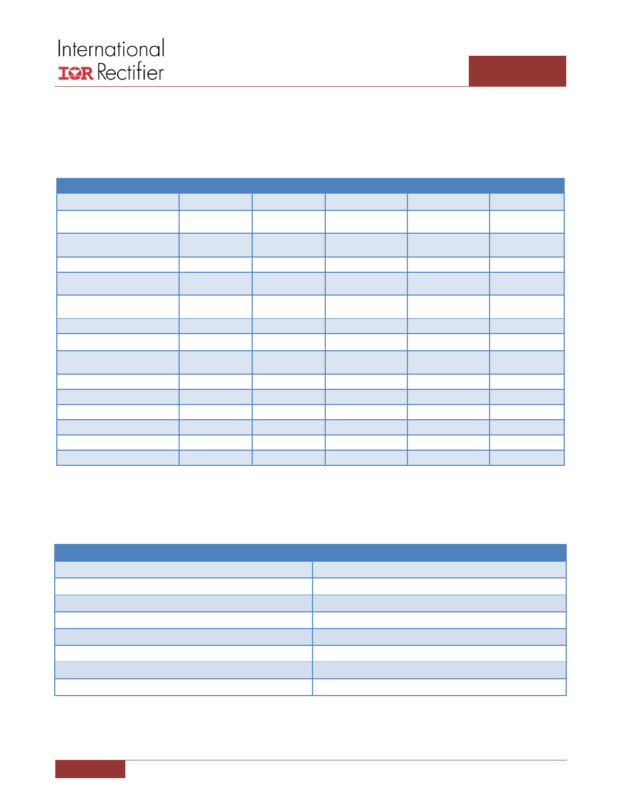
ABSOLUTE MAXIMUM RATINGS
Stresses beyond those listed under “Absolute Maximum Ratings” may cause permanent damage to the device. These are
stress ratings only and functional operation of the device at these or any other conditions beyond those indicated in the
operational sections of the specifications are not implied.
PIN Number
PIN NAME
V
MAX
V
MIN
I
SOURCE
I
SINK
1
VCC
6.5V
-0.3V
NA
10mA
2
LVCC
15V
-0.3V
NA
1A for 100ns,
100mA DC
3
HVCC
15V
-0.3V
NA
1A for 100ns,
100mA DC
4, 27
PGND
0.3V
-0.3V
15mA
15mA
5, 28
GATEL
LVCC + 0.3V
-3V for 20ns,
-0.3V DC
1A for 100ns,
200mA DC
1A for 100ns,
200mA DC
6-13
SW
2
25V
-5V for 20ns,
-0.3V DC
55A RMS
25A RMS
14, 15
PGND
NA
NA
25A RMS
55A RMS
16-19
VIN
2
25V
-0.3V
5A RMS
20A RMS
20
BOOST
1
35V
-0.3V
1A for 100ns,
100mA DC
5A for 100ns,
100mA DC
21
OT#
VCC + 0.3V
-0.3V
1mA
20mA
22
PWM
VCC + 0.3V
-0.3V
1mA
1mA
23
EN
VCC + 0.3V
-0.3V
1mA
1mA
24
LGND
0.3V
-0.3V
10mA
NA
25
MODE
VCC + 0.3V
-0.3V
1mA
1mA
26
OTSET
VCC + 0.3V
-0.3V
1mA
1mA
Note:
1. Maximum BOOST – SW = 15V.
2.
Maximum VIN – SW = 25V.
3. All the maximum voltage ratings are referenced to PGND (Pins 14 and 15).
THERMAL INFORMATION
Thermal Resistance, Junction to Top (θ
JC_TOP
)
18.2 °C/W
Thermal Resistance, Junction to PCB (pin 15) (θ
JB
)
2.6 °C/W
Thermal Resistance (θ
JA
)
1
20.8 °C/W
Maximum Operating Junction Temperature
-40 to 150°C
Maximum Storage Temperature Range
-65°C to 150°C
ESD rating
HBM Class 1A JEDEC Standard
MSL Rating
3
Reflow Temperature
260°C
Note:
1. Thermal Resistance (θ
JA
) is measured with the component mounted on a high effective thermal conductivity test board in free air.
Refer to International Rectifier Application Note AN-994 for details.
September 10, 2012 | FINAL DATASHEET
6
IR3558
45A Integrated PowIRstage®
ELECTRICAL SPECIFICATIONS
The electrical characteristics involve the spread of values guaranteed within the recommended operating conditions.
Typical values represent the median values, which are related to 25°C.
RECOMMENDED OPERATING CONDITIONS FOR RELIABLE OPERATION WITH MARGIN
PARAMETER
SYMBOL
MIN
MAX
UNIT
Recommended VIN Range
VIN
4.5
15
V
Recommended VCC Range
VCC
4.5
5.5
V
Recommended LVCC Range
LVCC
4.5
13.2
V
Recommended HVCC Range
HVCC
4.5
13.2
V
Recommended Switching Frequency
ƒ
SW
200
1000
kHz
Recommended Operating Junction Temperature
T
J
-40
125
°C
ELECTRICAL CHARACTERISTICS
PARAMETER
SYMBOL
CONDITIONS
MIN
TYP
MAX
UNIT
Efficiency
PowIRstage Peak Efficiency
η
Note 2, Figure 2
94.0
%
Note 3, Figure 8
93.0
%
PWM Tri-state Mode (Figure 6)
PWM Input High Threshold
V
PWM_HIGH
PWM Tri-state to High
2.0
2.5
3.0
V
PWM Input Low Threshold
V
PWM_LOW
PWM Tri-state to Low
0.7
0.8
0.9
V
PWM Tri-state Float Voltage
V
PWM_TRI
PWM Floating
0.85
1.60
2.55
V
Hysteresis
V
PWM_HYS
Active to Tri-state or Tri-
state to Active, Note 1
200
mV
Tri-state Hold OFF Time
T
PWM_HOLD
Note 1
80
ns
PWM Input Impedance
R
PWM_SINK
3.00
3.75
4.50
kΩ
Minimum Pulse Width
T
PWM_MIN
Note 1
40
60
ns
PWM Active Tri-Level (ATL) Mode (Figure 7)
PWM Input High Threshold
V
ATL_HIGH
0.8
1.0
1.2
V
PWM Input High Threshold
V
ATL_LOW
0.65
0.8
0.95
V
PWM Tri-Level High Voltage
V
ATL_TRI_HIGH
2.1
2.5
2.9
V
PWM Tri-Level Low Voltage
V
ATL_TRI_LOW
2.00
2.30
2.42
V
PWM Input Current Low
V
PWM
= 0V
-1.0
-1.5
mA
PWM Input Current High
V
PWM
= 1.8V
-1.0
-1.5
mA
Enable Input – EN
Input Voltage High
V
N_H
2.0
V
Input Voltage Low
V
EN_L
0.8
V
Input Current
I
EN
V(EN) = 5.5V
0.1
1
µA
September 10, 2012 | FINAL DATASHEET
7
IR3558
45A Integrated PowIRstage®
PARAMETER
SYMBOL
CONDITIONS
MIN
TYP
MAX
UNIT
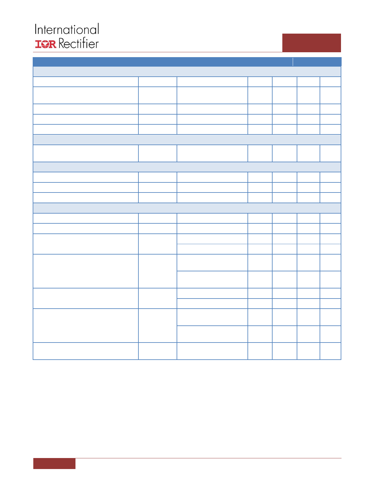
Thermal Warning - OTSET Input and OT# Output
Over Temperature High Threshold
OT
R
OTSET
= open, Note 1
150
°C
Programmable Over Temperature High
Threshold
OT
R
OTSET
= 100kΩ, Note 1
125
°C
Over Temperature Hysteresis
OT
HYS
Note 1
-20
°C
OT# Sink Current
1.0
1.5
mA
OT# Output Low Voltage
1.5mA
0.4
1.0
V
Bootstrap Diode
Forward Voltage
BD
FV
I(BOOST) = 30mA, LVCC =
6.8V
0.65
0.80
0.95
mV
VCC Under Voltage Lockout
Start Threshold
V
VCC_START
3.5
3.8
4.1
V
Stop Threshold
V
VCC_STOP
3.2
3.5
3.8
V
Hysteresis
V
VCC_HYS
0.15
0.30
0.45
V
General
VCC Supply Quiescent Current
I
VCC
V(VCC) = 5V, V(EN) =0V
1.5
2.5
mA
VCC Supply Current
I
VCC_SW
V(VCC) = 5V, V(EN) =5V
2.7
3.5
mA
LVCC Supply Quiescent Current
I
LVCC
V(LVCC) = 5V, V(EN) =0V
15
25
uA
V(LVCC) = 7V, V(EN) =0V
20
30
uA
LVCC Supply Current
I
LVCC_SW
V(LVCC) = 5V, V(EN) =5V,
fsw=400kHz
10
20
mA
V(LVCC) = 7V, V(EN) =5V,
fsw=400kHz
15
25
mA
HVCC Supply Quiescent Current
I
BOOST
V(HVCC) = 5V, V(EN) =0V
15
25
uA
V(HVCC) = 7V, V(EN) =0V
20
30
uA
HVCC Supply Current
I
BOOST_SW
V(HVCC) =5V, V(EN) =5V,
fsw=400kHz
5
10
mA
V(HVCC) =7V, V(EN) =5V,
fsw=400kHz
6.5
15
mA
VIN Supply Leakage Current
I
VIN
VIN = 20V, 125°C, V(PWM) =
Tri-State
1
µA
Notes
1. Guaranteed by design but not tested in production
2. V
IN
=12V, V
OUT
=1.2V, ƒ
SW
= 300kHz, L=210nH (0.2mΩ), HVCC=LVCC=6.8V, C
IN
=47uF x 4, C
OUT
=470uF x3, 400LFM airflow, no heat sink,
25°C ambient temperature, and 8-layer PCB of 3.7” (L) x 2.6” (W). PWM controller loss and inductor loss are not included.
3. V
IN
=12V, V
OUT
=1.2V, ƒ
SW
= 400kHz, L=150nH (0.29mΩ), HVCC=LVCC=7V, C
IN
=47uF x 4, C
OUT
=470uF x3, no airflow, no heat sink, 25°C
ambient temperature, and 8-layer PCB of 3.7” (L) x 2.6” (W). PWM controller loss and inductor loss are not included.
September 10, 2012 | FINAL DATASHEET
8
IR3558
45A Integrated PowIRstage®
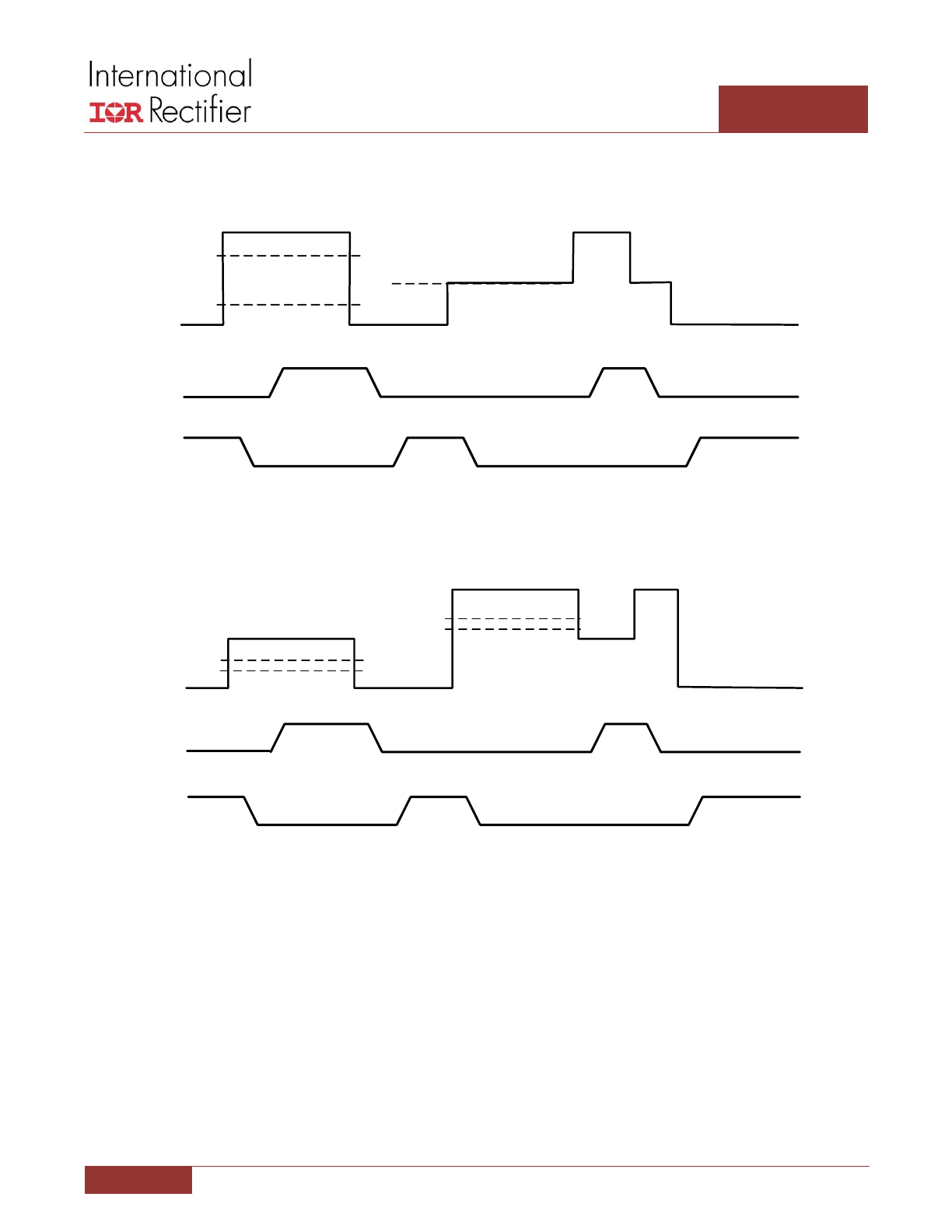
TIMING DIAGRAMS
Figure 6: IR3558 Switching Waveforms in 3.3V Tri-state PWM Mode
Figure 7: IR3558 Switching Waveforms in International Rectifier’s Active Tri-Level® (ATL) PWM Mode
GATEL
PWM
Normal PWM
ATL Tri-state
ATL Tri-state
Normal
PWM
V
ATL_HIGH
V
ATL_LOW
V
ATL_TRI_HIGH
V
ATL_TRI_LOW
SW
PWM
SW
GATEL
Normal PWM
Tri-state
Tri-state
V
PWM_HIGH
V
PWM_LOW
V
PWM_TRI
Normal PWM
September 10, 2012 | FINAL DATASHEET
9
IR3558
45A Integrated PowIRstage®
TYPICAL OPERATING CHARACTERISTICS
Circuit of Figure 32, V
IN
=12V, V
OUT
=1.2V, ƒ
SW
=400kHz, L=150nH (0.29mΩ), VCC=5V, HVCC=LVCC=7V, T
AMB
=25°C, no heat sink,
no air flow, 8-layer PCB board of 3.7” (L) x 2.6” (W), no PWM controller loss, no inductor loss, unless specified otherwise.
Figure 8: Typical IR3558 Efficiency
Figure 9: Typical IR3558 Power Loss
Figure 10: Safe Operating Area, T
CASE
<= 125°C
Figure 11: Normalized Power Loss vs. Input Voltage
Figure 12: Normalized Power Loss vs. Output Voltage
Figure 13: Normalized Power Loss vs. Switching Frequency
80
81
82
83
84
85
86
87
88
89
90
91
92
93
94
0
5
10
15
20
25
30
35
40
Output Current (A)
Ef
fi
ci
en
cy
(
%
)
0
1
2
3
4
5
6
7
8
9
10
0
5
10
15
20
25
30
35
40
Output Current (A)
P
o
w
er
L
o
ss
(
W
)
0.80
0.85
0.90
0.95
1.00
1.05
1.10
1.15
1.20
1.25
1.30
1.35
1.40
0.8
0.9
1
1.1
1.2
1.3
1.4
1.5
1.6
1.7
1.8
1.9
2
Output Voltage (V)
N
or
m
al
iz
ed
P
ower
L
os
s
-4.4
-3.3
-2.2
-1.1
0.0
1.1
2.2
3.3
4.4
5.5
6.6
7.7
8.8
Ca
se
Tem
per
at
ur
e
A
dj
us
tm
en
t
(°
C)
0.85
0.90
0.95
1.00
1.05
1.10
1.15
5
6
7
8
9
10
11
12
13
14
15
Input Voltage (V)
N
o
rma
liz
ed
P
o
w
er
L
o
ss
-3.3
-2.2
-1.1
0.0
1.1
2.2
3.3
Ca
se
T
emp
er
atu
re
A
d
ju
stme
n
t
(°
C)
0.85
0.90
0.95
1.00
1.05
1.10
1.15
1.20
1.25
1.30
1.35
1.40
1.45
200
300
400
500
600
700
800
900
1000
Switching Frequency (kHz)
N
o
rma
liz
ed
P
o
w
er
L
o
ss
-3.3
-2.2
-1.1
0.0
1.1
2.2
3.3
4.4
5.5
6.6
7.7
8.8
9.9
Ca
se
Tem
per
at
ur
e
A
dj
us
tm
en
t
(°
C)
0
5
10
15
20
25
30
35
40
45
50
0
5
10 15 20 25 30 35 40 45 50 55 60 65 70 75 80 85 90
Ambient Temperature (°C)
O
ut
pu
t
C
ur
ren
t
(A
)
400LFM
200LFM
100LFM
0LFM
September 10, 2012 | FINAL DATASHEET
10
IR3558
45A Integrated PowIRstage®
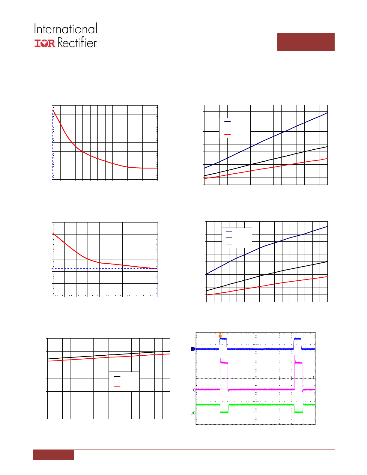
TYPICAL OPERATING CHARACTERISTICS (CONTINUED)
Circuit of Figure 32, V
IN
=12V, V
OUT
=1.2V, ƒ
SW
=400kHz, L=150nH (0.29mΩ), VCC=5V, HVCC=LVCC=7V, T
AMB
=25°C, no heat sink,
no air flow, 8-layer PCB board of 3.7” (L) x 2.6” (W), no PWM controller loss, no inductor loss, unless specified otherwise.
Figure 14: Normalized Power Loss vs. HVCC & LVCC Voltage
Figure 15: Power Loss vs. Output Inductor
0.0
0.5
1.0
1.5
2.0
2.5
3.0
200
250
300
350
400
450
500
550
600
650
700
750
800
850
900
950 1000
fsw (kHz)
V
C
C
C
u
rr
en
t
(m
A
)
Vcc=5.5V
Vcc=5V
Figure 16: VCC Current vs. Switching Frequency
0
5
10
15
20
25
30
35
40
45
50
55
60
200
250
300
350
400
450
500
550
600
650
700
750
800
850
900
950 1000
fsw (kHz)
LV
C
C
C
u
rr
en
t
(m
A
)
LVCC=12V
LVCC=7V
LVCC=5V
Figure 17: LVCC Current vs. Switching Frequency
0.0
2.5
5.0
7.5
10.0
12.5
15.0
17.5
20.0
22.5
25.0
27.5
30.0
200
250
300
350
400
450
500
550
600
650
700
750
800
850
900
950 1000
fsw (kHz)
LV
C
C
C
u
rr
en
t
(m
A
)
HVCC=12V
HVCC=7V
HVCC=5V
Figure 18: HVCC Current vs. Switching Frequency
Figure 19: Switching Waveform in Tri-state Mode, I
OUT
= 0A
PWM
5V/div
SW
5V/div
GATEL
10V/div
400ns/div
0.85
0.90
0.95
1.00
1.05
1.10
1.15
1.20
1.25
5.0 5.5 6.0 6.5 7.0 7.5 8.0 8.5 9.0 9.5 10.0 10.5 11.0 11.5 12.0
HVCC and LVCC Voltage (V)
N
o
rma
liz
ed
P
o
w
er
L
o
ss
-3.3
-2.2
-1.1
0.0
1.1
2.2
3.3
4.4
5.5
Ca
se
T
emp
er
atu
re
A
d
ju
stme
n
t
(°
C)
0.85
0.90
0.95
1.00
1.05
1.10
1.15
120
130
140
150
160
170
180
190
200
210
Output Inductor (nH)
N
o
rma
liz
ed
P
o
w
er
L
o
ss
-3.3
-2.2
-1.1
0.0
1.1
2.2
3.3
Ca
se
T
emp
er
atu
re
A
d
ju
stme
n
t
(°
C)