
July 16, 2014 | DATASHEET V3.3
1
IR3553
40A Integrated PowIRstage®
FEATURES
Peak efficiency up to 93.2% at 1.2V
Integrated driver, control MOSFET, synchronous
MOSFET and Schottky diode
Input voltage (VIN) operating range up to 15V
Output voltage range from 0.25V to Vcc-2.5V, or to
5.5V if internal current sense amplifier is not used
Output current capability of 40A DC
Operation up to 1.0MHz
Integrated current sense amplifier
VCC under voltage lockout
Thermal flag
Body-Braking® load transient support
Diode-emulation high efficiency mode
Compatible with 3.3V PWM logic and VCC tolerant
Compliant with Intel DrMOS V4.0
PCB footprint compatible with IR3550 and IR3551
Efficient dual sided cooling
Small 4mm x 6mm x 0.9mm PQFN package
Lead free RoHS compliant package
APPLICATIONS
Voltage Regulators for CPUs, GPUs, and DDR
memory arrays
High current, low profile DC-DC converters
BASIC APPLICATION
SW
PWM
VIN
PGND
VCC
VCC
BOOST
VIN
VOUT
PWM
CSIN+
CSIN-
4.5V to 7V
LGND
IOUT
IOUT
BBRK#
BBRK#
REFIN
REFIN
4.5V to 15V
IR3553
PHSFLT#
PHSFLT#
Figure 1: IR3553 Basic Application Circuit
DESCRIPTION
The IR3553 integrated PowIRstage® is a synchronous buck
gate driver co-packed with a control MOSFET and a
synchronous MOSFET with integrated Schottky diode. It is
optimized internally for PCB layout, heat transfer and
driver/MOSFET timing. Custom designed gate driver and
MOSFET combination enables higher efficiency at lower
output voltages required by cutting edge CPU, GPU and
DDR memory designs.
Up to 1.0MHz switching frequency enables high
performance transient response, allowing miniaturization
of output inductors, as well as input and output capacitors
while maintaining industry leading efficiency. The IR3553’s
superior efficiency enables smallest size and lower solution
cost. The IR3553 PCB footprint is compatible with the
IR3550 (60A) and the IR3551 (50A).
Integrated current sense amplifier achieves superior
current sense accuracy and signal to noise ratio vs. best-in-
class controller based Inductor DCR sense methods.
The IR3553 incorporates the Body- Braking® feature which
enables reduction of output capacitors. Synchronous diode
emulation mode in the IR3553 removes the zero-current
detection burden from the PWM controller and increases
system light-load efficiency.
The IR3553 is optimized specifically for CPU core power
delivery in server applications. The ability to meet the
stringent requirements of the server market also makes
the IR3553 ideally suited to powering GPU and DDR
memory designs and other high current applications.
Figure 2: Typical IR3553 Efficiency & Power Loss
(See Note 2 on Page 8)
74
76
78
80
82
84
86
88
90
92
94
0
5
10
15
20
25
30
35
40
Output Current (A)
Ef
fi
ci
en
cy
(
%
)
0
2
4
6
8
10
12
14
16
18
20
P
o
w
er
L
o
ss
(
W
)
July 16, 2014 | DATASHEET V3.3
2
IR3553
40A Integrated PowIRstage®
PINOUT DIAGRAM
Figure 3: IR3553 Pin Diagram, Top View
ORDERING INFORMATION
Package
Tape & Reel Qty
Part Number
PQFN, 25 Lead
4mm x 6mm
3000
IR3553MTRPBF
Package
Qty
Part Number
PQFN, 25 Lead
4mm x 6mm
100
IR3553MPBF
TYPICAL APPLICATION DIAGRAM
SW
PWM
VIN
PGND
Gate
Drivers
and
Current
Sense
Amplifier
LGND
VCC
PHSFLT#
IOUT
VCC
BOOST
VIN
PWM
IOUT
PHSFLT#
BBRK#
BBRK#
REFIN
REFIN
CSIN-
CSIN+
IR3553
4.5V to 7V
4.5V to 15V
C2
10uF x 2
C5
0.22uF
C3
1uF
R1
10k
C4
0.22uF
R2
2.49k
L1
150nH
3
14-16
17
18
19
20
22
21
23
1
2
12, 13
6-11
C1
0.22uF
PGND 4
24
TGND
No Connect
C8
1nF
C9
22nF
Optional for
diode emulation
setup
VOUT
C7
470uF
C6
22uF
Figure 4: Application Circuit with Current Sense Amplifier
July 16, 2014 | DATASHEET V3.3
3
IR3553
40A Integrated PowIRstage®
TYPICAL APPLICATION DIAGRAM (CONTINUED)
SW
PWM
VIN
PGND
Gate
Drivers
and
Current
Sense
Amplifier
IOUT
VCC
PHSFLT#
VCC
BOOST
VIN
PWM
REFIN
PHSFLT#
BBRK#
BBRK#
CS+
LGND
CSIN-
CSIN+
IR3553
4.5V to 7V
4.5V to 15V
C2
10uF x 2
C5
0.22uF
C3
0.22uF
R1
10k
C4
0.22uF
R2
2.49k
L1
150nH
3
14-16
17
18
19
20
21
23
22
1
2
12, 13
6-11
C1
0.22uF
PGND 4
24
TGND
No Connect
CS-
VOUT
C7
470uF
C6
22uF
Figure 5: Application Circuit without Current Sense Amplifier
FUNCTIONAL BLOCK DIAGRAM
PW M
6
7
8
9
10
11
14
15
16
VIN
VIN
VIN
SW
SW
SW
SW
SW
SW
1
4
12
13
CSIN -
PG N D
PG N D
PG N D
17
BO O ST
Pow er-on
Reset
(PO R),
3.3V
Reference,
and
D ead-tim e
Control
19
IO U T
23
VCC
3
BBRK#
20
25
5
G ATEL G ATEL
D river
D river
18
PH SFLT#
2
CSIN +
21
LG N D
22
REFIN
Current Sense
Am plifier
M O SFET
& Therm al
D etection
S Q
R
PO R
3.3V
VCC
-
+
3.3V
24
TG N D
Figure 6: IR3553 Functional Block Diagram
July 16, 2014 | DATASHEET V3.3
4
IR3553
40A Integrated PowIRstage®
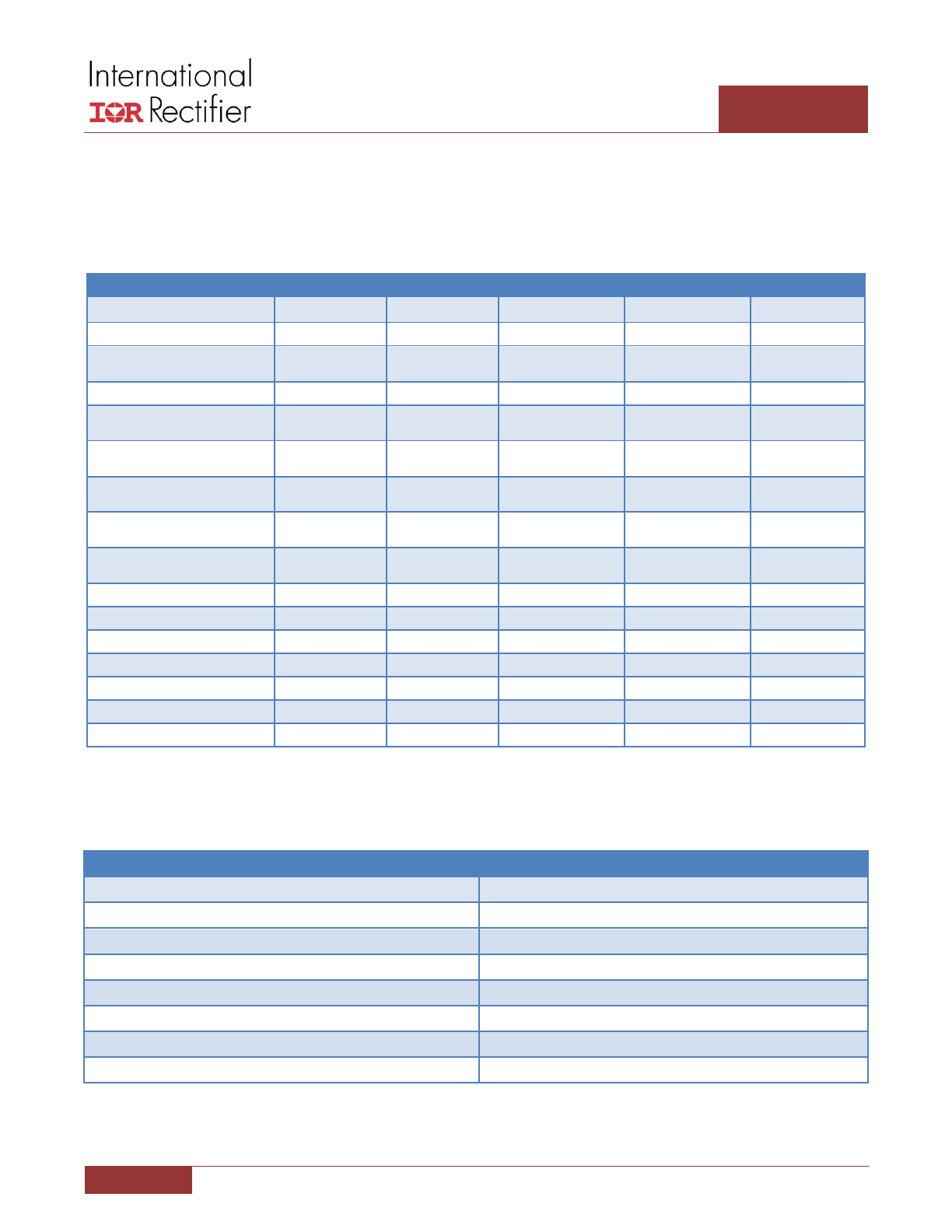
PIN DESCRIPTIONS
PIN #
PIN NAME
PIN DESCRIPTION
1
CSIN-
Inverting input to the current sense amplifier. Connect to LGND if the current sense
amplifier is not used.
2
CSIN+
Non-Inverting input to the current sense amplifier. Connect to LGND if the current sense
amplifier is not used.
3
VCC
Bias voltage for control logic. Connect a minimum 1uF cap between VCC and PGND (pin
4) if current sense amplifier is used. Connect a minimum 0.22uF capacitor between VCC
and PGND (pin 4) if current sense amplifier is not used.
4, 12, 13
PGND
Power ground of MOSFET driver and the synchronous MOSFET. MOSFET driver signal is
referenced to this pin.
5, 25
GATEL
Low-side MOSFET driver pins that can be connected to a test point in order to observe
the waveform.
6 – 11
SW
Switch node of synchronous buck converter.
14 – 16
VIN
High current input voltage connection. Recommended operating range is 4.5V to 15V.
Connect at least two 10uF 1206 ceramic capacitors and a 0.22uF 0402 ceramic
capacitor. Place the capacitors as close as possible to VIN pins and PGND pins (12-13).
The 0.22uF 0402 capacitor should be on the same side of the PCB as the IR3553.
17
BOOST
Bootstrap capacitor connection. The bootstrap capacitor provides the charge to turn on
the control MOSFET. Connect a minimum 0.22µF capacitor from BOOST to SW pin. Place
the capacitor as close to BOOST pin as possible and minimize parasitic inductance of
PCB routing from the capacitor to SW pin.
18
PHSFLT#
Open drain output of the phase fault circuits. Connect to an external pull-up resistor.
Output is low when a MOSFET fault or over temperature condition is detected.
19
PWM
3.3V logic level tri-state PWM input and 7V tolerant. “High” turns the control MOSFET
on, and “Low” turns the synchronous MOSFET on. “Tri-state” turns both MOSFETs off in
Body-Braking® mode. In diode emulation mode, “Tri-state” activates internal diode
emulation control. See “PWM Tri-state Input” Section for further details about the PWM
Tri-State functions.
20
BBRK#
3.3V logic level input and 7V tolerant with internal weak pull-up to 3.3V. Logic low
disables both MOSFETs. Pull up to VCC directly or by a 4.7kΩ resistor if Body-Braking® is
not used. The second function of the BBRK# pin is to select diode emulatiom mode.
Pulling BBRK# low at least 20ns after VCC passes its UVLO threshold selects internal
diode emulation control. See “Body-Braking
®
Mode” Section for further details.
21
LGND
Signal ground. Driver control logic, analog circuits and IC substrate are referenced to
this pin.
22
REFIN
Reference voltage input from the PWM controller. IOUT signal is referenced to the
voltage on this pin. Connect to LGND if the current sense amplifier is not used.
23
IOUT
Current output signal. Voltage on this pin is equal to V(REFIN) + 32.5 * [V(CSIN+) –
V(CSIN-)]. Float this pin if the current sense amplifier is not used.
24
TGND
This pin is connected to internal power and signal ground of the driver. For best
performance of the current sense amplifier, TGND must be electrically isolated from
Power Ground (PGND) and Signal Ground (LGND) in the PCB layout. Connect to PGND if
the current sense amplifier is not used.
July 16, 2014 | DATASHEET V3.3
5
IR3553
40A Integrated PowIRstage®
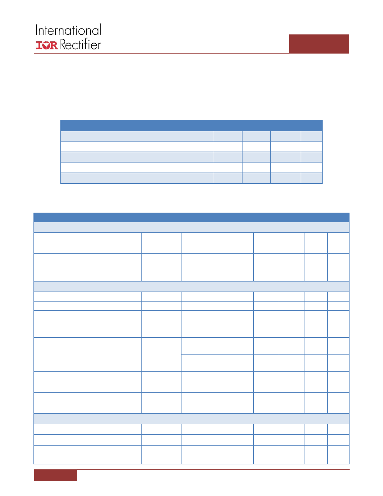
ABSOLUTE MAXIMUM RATINGS
Stresses beyond those listed under “Absolute Maximum Ratings” may cause permanent damage to the device. These are
stress ratings only and functional operation of the device at these or any other conditions beyond those indicated in the
operational sections of the specifications are not implied.
PIN Number
PIN NAME
V
MAX
V
MIN
I
SOURCE
I
SINK
1
CSIN-
VCC + 0.3V
-0.3V
1mA
1mA
2
CSIN+
VCC + 0.3V
-0.3V
1mA
1mA
3
VCC
8V
-0.3V
NA
5A for 100ns,
200mA DC
4
PGND
0.3V
-0.3V
15mA
15mA
5, 25
GATEL
VCC + 0.3V
-3V for 20ns,
-0.3V DC
1A for 100ns,
200mA DC
1A for 100ns,
200mA DC
6-11
SW
2
25V
-5V for 20ns,
-0.3V DC
45A RMS,
60A Peak
20A RMS,
25A Peak
12, 13
PGND
NA
NA
20A RMS,
25A Peak
45A RMS,
60A Peak
14-16
VIN
2
25V
-0.3V
5A RMS
15A RMS,
20A Peak
17
BOOST
1
33V
-0.3V
1A for 100ns,
100mA DC
5A for 100ns,
100mA DC
18
PHSFLT#
VCC + 0.3V
-0.3V
1mA
20mA
19
PWM
VCC + 0.3V
-0.3V
1mA
1mA
20
BBRK#
VCC + 0.3V
-0.3V
1mA
1mA
21
LGND
0.3V
-0.3V
15mA
15mA
22
REFIN
3.5V
-0.3V
1mA
1mA
23
IOUT
VCC + 0.3V
-0.3V
5mA
5mA
24
TGND
0.3V
-0.3V
NA
NA
Note:
1. Maximum BOOST – SW = 8V.
2.
Maximum VIN – SW = 25V.
3. All the maximum voltage ratings are referenced to PGND (Pins 12 and 13).
THERMAL INFORMATION
Thermal Resistance, Junction to Top (θ
JC_TOP
)
23.2 °C/W
Thermal Resistance, Junction to PCB (pin 13) (θ
JB
)
2.5 °C/W
Thermal Resistance (θ
JA
)
1
22.2 °C/W
Maximum Operating Junction Temperature
-40 to 150°C
Maximum Storage Temperature Range
-65°C to 150°C
ESD rating
HBM Class 1B JEDEC Standard
MSL Rating
3
Reflow Temperature
260°C
Note:
1. Thermal Resistance (θ
JA
) is measured with the component mounted on a high effective thermal conductivity test board in free air.
Refer to International Rectifier Application Note AN-994 for details.
July 16, 2014 | DATASHEET V3.3
6
IR3553
40A Integrated PowIRstage®
ELECTRICAL SPECIFICATIONS
The electrical characteristics involve the spread of values guaranteed within the recommended operating conditions.
Typical values represent the median values, which are related to 25°C.
RECOMMENDED OPERATING CONDITIONS FOR RELIABLE OPERATION WITH MARGIN
PARAMETER
SYMBOL
MIN
MAX
UNIT
Recommended VIN Range
VIN
4.5
15
V
Recommended VCC Range
VCC
4.5
7
V
Recommended REFIN Range
REFIN
0.25
VCC – 2.5
V
Recommended Switching Frequency
ƒ
SW
200
1000
kHz
Recommended Operating Junction Temperature
T
J
-40
125
°C
ELECTRICAL CHARACTERISTICS
PARAMETER
SYMBOL
CONDITIONS
MIN
TYP
MAX
UNIT
Efficiency and Maximum Current
IR3553 Peak Efficiency
Note 1
η
Note 2. See Figure 2.
92.7
%
Note 3. See Figure 7.
92.2
%
IR3553 Maximum DC Current
Note 1
I
DC_MAX
Note 2.
40
A
IR3553 Maximum Peak Current
Note 1
I
PK_MAX
Note 4. 5ms load pulse
width, 10% load duty cycle.
60
A
PWM Comparator
PWM Input High Threshold
V
PWM_HIGH
PWM Tri-state to High
2.5
V
PWM Input Low Threshold
V
PWM_LOW
PWM Tri-state to Low
0.8
V
PWM Tri-state Float Voltage
V
PWM_TRI
PWM Floating
1.2
1.65
2.1
V
Hysteresis
V
PWM_HYS
Active to Tri-state or Tri-
state to Active, Note 1
65
76
100
mV
Tri-state Propagation Delay
t
PWM_DELAY
PWM Tri-state to Low
transition to GATEL >1V
38
ns
PWM Tri-state to High
transition to GATEH >1V
18
ns
PWM Sink Impedance
R
PWM_SINK
3.67
5.1
8.70
kΩ
PWM Source Impedance
R
PWM_SOURCE
3.67
5.1
8.70
kΩ
Internal Pull up Voltage
V
PWM_PULLUP
VCC > UVLO
3.3
V
Minimum Pulse Width
t
PWM_MIN
Note 1
41
58
ns
Current Sense Amplifier
CSIN+/- Bias Current
I
CSIN_BIAS
-100
0
100
nA
CSIN+/- Bias Current Mismatch
I
CSIN_BIASMM
-50
0
50
nA
Calibrated Input Offset Voltage
V
CSIN_OFFSET
Self-calibrated offset,
0.5V ≤ V(REFIN) ≤ 2.25V
±450
µV
July 16, 2014 | DATASHEET V3.3
7
IR3553
40A Integrated PowIRstage®
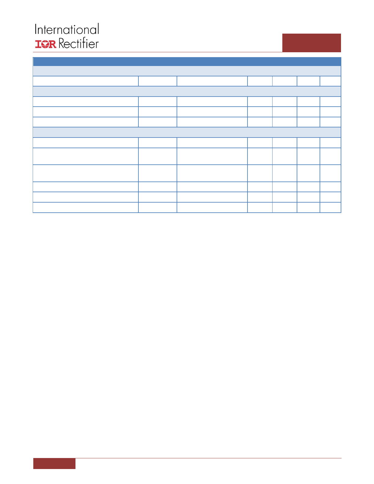
PARAMETER
SYMBOL
CONDITIONS
MIN
TYP
MAX
UNIT
Gain
G
CS
0.5V ≤ V(REFIN) ≤ 2.25V,
-5mV ≤ *V(CSIN+) –V(CSIN-)]
≤ 25mV, 0°C ≤ T
J
≤ 125°C
30.0
32.5
35.0
V/V
0.5V ≤ V(REFIN) ≤ 2.25V,
-5mV ≤ *V(CSIN+) – V(CSIN-)]
≤ 25mV
30.0
33.0
36.0
V/V
0.8V ≤ V(REFIN) ≤ 2.25V,
-10mV ≤*V(CSIN+)–V(CSIN-)]
≤ 25mV
28.0
31.5
35.0
V/V
Unity Gain Bandwidth
f
BW
C(IOUT) = 10pF. Measure at
IOUT. Note 1
4.8
6.8
8.8
MHz
Slew Rate
S
R
6
V/µs
Differential Input Range
V
D_IN
0.8V ≤ V(REFIN) ≤ 2.25V,
-10
25
mV
Common Mode Input Range
V
C_IN
0
VCC-
2.5
V
Output Impedance (IOUT)
R
CS_OUT
62
200
Ω
IOUT Sink Current
I
CS_SINK
Driving external 3 kΩ
0.5
0.8
1.1
mA
Diode Emulation Mode Comparator
Input Offset Voltage
V
IN_OFFSET
Note 1
-12
-3
3
mV
Leading Edge Blanking Time
t
BLANK
V(GATEL)>1V Starts Timer
50
150
200
ns
Negative Current Time-Out
t
NC_TOUT
PWM = Tri-State,
V(SW) ≤ -10mV
12
28
46
µs
Digital Input – BBRK#
Input voltage high
V
BBRK#_IH
2.0
V
Input voltage low
V
BBRK#_IL
0.8
V
Internal Pull Up Resistance
R
BBRK#_PULLUP
VCC > UVLO
69
200
338
kΩ
Internal Pull Up Voltage
V
BBRK#_PULLUP
VCC > UVLO
3.3
V
Digital Output – PHSFLT#
Output voltage high
V
PHASFLT#_OH
VCC
V
Output voltage low
V
PHASFLT#_OL
4mA
150
300
mV
Input current
I
PHASFLT#_IN
V(PHSFLT#) = 5.5V
0
1
µA
Phase Fault Detection
Control MOSFET Short Threshold
V
CM_SHORT
Measure from SW to PGND
3.3
V
Synchronous MOSFET Short Threshold
V
SM_SHORT
Measure from SW to PGND
150
200
250
mV
Synchronous MOSFET Open Threshold
V
SM_OPEN
Measure from SW to PGND
-250
-200
-150
mV
Propagation Delay
t
PROP
PWM High to Low Cycles
15
Cycle
Thermal Flag
Rising Threshold
T
RISE
PHSFLT# Drives Low,
Note 1
160
°C
Falling Threshold
T
FALL
Note 1
135
°C
July 16, 2014 | DATASHEET V3.3
8
IR3553
40A Integrated PowIRstage®
PARAMETER
SYMBOL
CONDITIONS
MIN
TYP
MAX
UNIT
Bootstrap Diode
Forward Voltage
V
FWD
I(BOOST) = 30mA, VCC=6.8V
360
520
920
mV
VCC Under Voltage Lockout
Start Threshold
V
VCC_START
3.3
3.7
4.1
V
Stop Threshold
V
VCC_STOP
3.0
3.4
3.8
V
Hysteresis
V
VCC_HYS
0.2
0.3
0.4
V
General
VCC Supply Current
I
VCC
VCC = 4.5V to 7V
4
8
12
mA
VIN Supply Leakage Current
I
VIN
VIN = 20V, 125C, V(PWM) =
Tri-State
1
µA
BOOST Supply Current
I
BOOST
4.75V < V(BOOST)-V(SW) <
8V
0.5
1.5
3.0
mA
REFIN Bias Current
I
REFIN
-1.5
0
1
µA
SW Floating Voltage
V
SW_FLOAT
V(PWM) = Tri-State
0.2
0.4
V
SW Pull Down Resistance
R
SW_PULLDOWN
BBRK# is Low or VCC = 0V
18
kΩ
Notes
1. Guaranteed by design but not tested in production
2. V
IN
=12V, V
OUT
=1.2V, ƒ
SW
= 300kHz, L=210nH (0.2mΩ), VCC=6.8V, C
IN
=47uF x 4, C
OUT
=470uF x3, 400LFM airflow, no heat sink, 25°C
ambient temperature, and 8-layer PCB of 3.7” (L) x 2.6” (W). PWM controller loss and inductor loss are not included.
3. V
IN
=12V, V
OUT
=1.2V, ƒ
SW
= 400kHz, L=150nH (0.29mΩ), VCC=7V, C
IN
=47uF x 4, C
OUT
=470uF x3, no airflow, no heat sink, 25°C ambient
temperature, and 8-layer PCB of 3.7” (L) x 2.6” (W). PWM controller loss and inductor loss are not included.
4. V
IN
=12V, V
OUT
=1.2V, ƒ
SW
= 400kHz, L=210nH (0.2mΩ, 13mm x 13mm x 8mm), VCC=6.8V, C
IN
=47uF x 4, C
OUT
=470uF x3, no heat sink,
25°C ambient temperature, 8-layer PCB of 3.7” (L) x 2.6” (W), 5ms load pulse width, 10% load duty cycle, and IR3553 junction
temperature below 125°C.
July 16, 2014 | DATASHEET V3.3
9
IR3553
40A Integrated PowIRstage®
TYPICAL OPERATING CHARACTERISTICS
Circuit of Figure 32, V
IN
=12V, V
OUT
=1.2V, ƒ
SW
= 400kHz, L=150nH (0.29mΩ), VCC=7V, T
AMBIENT
= 25°C, no heat sink, no air flow,
8-layer PCB board of 3.7” (L) x 2.6” (W), no PWM controller loss, no inductor loss, unless specified otherwise.
Figure 7: Typical IR3553 Efficiency
Figure 8: Typical IR3553 Power Loss
Figure 9: Thermal Derating Curve, T
CASE
<= 125°C
Figure 10: Normalized Power Loss vs. Input Voltage
Figure 11: Normalized Power Loss vs. Output Voltage
Figure 12: Normalized Power Loss vs. Switching Frequency
80
81
82
83
84
85
86
87
88
89
90
91
92
93
0
5
10
15
20
25
30
35
40
Output Current (A)
Ef
fi
ci
en
cy
(
%
)
0
1
2
3
4
5
6
7
8
9
10
0
5
10
15
20
25
30
35
40
Output Current (A)
P
o
w
er
L
o
ss
(
W
)
0.80
0.85
0.90
0.95
1.00
1.05
1.10
1.15
1.20
1.25
1.30
5
6
7
8
9
10
11
12
13
14
15
Input Voltage (V)
N
o
rm
a
liz
ed
P
o
wer
L
o
ss
-6.0
-4.5
-3.0
-1.5
0.0
1.5
3.0
4.5
6.0
7.5
9.0
C
a
se
T
em
p
er
a
tu
re
A
d
ju
st
m
en
t
(°
C
)
0.8
0.9
1.0
1.1
1.2
1.3
1.4
1.5
0.8
0.9
1
1.1
1.2
1.3
1.4
1.5
1.6
1.7
1.8
1.9
2
Output Voltage (V)
N
o
rm
a
liz
ed
P
o
wer
L
o
ss
-6
-3
0
3
6
9
12
15
C
a
se
T
em
p
er
a
tu
re
A
d
ju
st
m
en
t
(°
C
)
0.80
0.85
0.90
0.95
1.00
1.05
1.10
1.15
1.20
1.25
1.30
200
300
400
500
600
700
800
900
1000
Switching Frequency (kHz)
N
o
rma
liz
ed
P
o
w
er
L
o
ss
-6.0
-4.5
-3.0
-1.5
0.0
1.5
3.0
4.5
6.0
7.5
9.0
C
a
se
T
em
p
er
a
tu
re
A
d
ju
st
m
en
t
(°
C
)
July 16, 2014 | DATASHEET V3.3
10
IR3553
40A Integrated PowIRstage®
TYPICAL OPERATING CHARACTERISTICS (CONTINUED)
Circuit of Figure 32, V
IN
=12V, V
OUT
=1.2V, ƒ
SW
= 400kHz, L=150nH (0.29mΩ), VCC=7V, T
AMBIENT
= 25°C, no heat sink, no air flow,
8-layer PCB board of 3.7” (L) x 2.6” (W), no PWM controller loss, no inductor loss, unless specified otherwise.
Figure 13: Normalized Power Loss vs. VCC Voltage
Figure 14: Power Loss vs. Output Inductor
Figure 15: VCC Current vs. Switching Frequency
Figure 16: Switching Waveform, I
OUT
= 0A
Figure 17: Switching Waveform, I
OUT
= 40A
Figure 18: PWM to SW Delays, I
OUT
= 10A
PWM
2V/div
SW
5V/div
40ns/div
PWM
5V/div
SW
5V/div
GATEL
10V/div
400ns/div
PWM
5V/div
SW
5V/div
GATEL
10V/div
400ns/div
0
10
20
30
40
50
60
200
300
400
500
600
700
800
900
1000
fsw (kHz)
V
CC
Cu
rr
en
t
(mA
)
Vcc=6.8V
Vcc=5V
0.80
0.85
0.90
0.95
1.00
1.05
1.10
1.15
1.20
1.25
1.30
5.00
5.25
5.50
5.75
6.00
6.25
6.50
6.75
7.00
VCC Voltage (V)
N
o
rma
liz
ed
P
o
w
er
L
o
ss
-6.0
-4.5
-3.0
-1.5
0.0
1.5
3.0
4.5
6.0
7.5
9.0
Ca
se
T
emp
er
atu
re
A
d
ju
stme
n
t
(°
C)
0.80
0.85
0.90
0.95
1.00
1.05
1.10
1.15
1.20
1.25
1.30
120
130
140
150
160
170
180
190
200
210
Output Inductor (nH)
N
o
rma
liz
ed
P
o
w
er
L
o
ss
-6.0
-4.5
-3.0
-1.5
0.0
1.5
3.0
4.5
6.0
7.5
9.0
Ca
se
T
emp
er
atu
re
A
d
ju
stme
n
t
(°
C)