
www.irf.com
© 2009 International Rectifier
September 26, 2011
IR1168S
DUAL SMART RECTIFIER DRIVER IC
Features
•
Secondary-side
high
speed
controller
for
synchronous rectification in resonant half bridge
topologies
•
200V proprietary IC technology
•
Max 500KHz switching frequency
•
Anti-bounce logic and UVLO protection
•
4A peak turn off drive current
•
Micropower start-up & ultra low quiescent current
•
10.7V gate drive clamp
•
70ns turn-off propagation delay
•
Wide Vcc operating range
•
Direct sensing for both Synchronous Rectifiers
•
Minimal component count
•
Simple design
•
Lead-free
Typical Applications
•
LCD & PDP TV, Telecom SMPS, AC-DC adapters
Product Summary
Topology
LLC Half-bridge
VD
200V
V
OUT
10.7V Clamped
I
o+
& I
o-
(typical)
+1A & -4A
Turn on Propagation Delay
60ns (typical)
Turn off Propagation Delay
70ns (typical)
Package Options
8-Lead SOIC
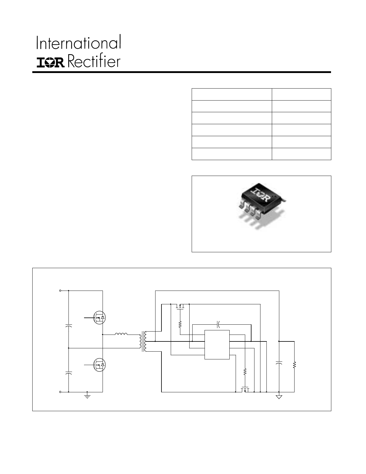
Typical Connection Diagram
LOAD
SR1
SR2
Cdc
1
2
Lr
C1
C2
Rtn
Vin
VD2
5
VS2
6
VS1
3
VCC
2
VD1
4
GND
7
GATE2
8
GATE1
1
IR1168
Cout
Rg2
Rg1
M1
M2
Datasheet No – PD97382
IR1168
IR1168S
www.irf.com
© 2009 International Rectifier
2
Table of Contents
Page
Description
3
Qualification Information
4
Absolute Maximum Ratings
5
Electrical Characteristics
6
Functional Block Diagram
8
Input/Output Pin Equivalent Circuit Diagram
9
Lead Definitions
10
Lead Assignments
10
Application Information and Additional Details
12
Package Details
16
Tape and Reel Details
17
Part Marking Information
18
Ordering Information
19

IR1168S
www.irf.com
© 2009 International Rectifier
3
Description
IR1168 is dual smart secondary-side rectifier driver IC designed to drive two N-Channel power MOSFETs used as
synchronous rectifiers in resonant converter applications. The IC can control one or more paralleled N MOSFETs
to emulate the behavior of Schottky diode rectifiers. The drain to source for each rectifier MOSFET voltage is
sensed differentially to determine the level of the current and the power switch is turned ON and OFF in close
proximity of the zero current transition. Ruggedness and noise immunity are accomplished using an advanced
blanking scheme and double-pulse suppression that allows reliable operation in fixed and variable frequency
applications.
IR1168S
www.irf.com
© 2009 International Rectifier
4
Qualification Information
†
Qualification Level
Industrial
††
Comments: This family of ICs has passed JEDEC’s
Industrial qualification. IR’s Consumer qualification level is
granted by extension of the higher Industrial level.
Moisture Sensitivity Level
SOIC8N
MSL2
†††
260°C
(per IPC/JEDEC J-STD-020)
ESD
Machine Model
Class B
(per JEDEC standard JESD22-A115)
Human Body Model
Class 2
(per EIA/JEDEC standard EIA/JESD22-A114)
IC Latch-Up Test
Class I, Level A
(per JESD78)
RoHS Compliant
Yes
†
Qualification standards can be found at International Rectifier’s web site
http://www.irf.com/
††
Higher qualification ratings may be available should the user have such requirements. Please contact
your International Rectifier sales representative for further information.
††† Higher MSL ratings may be available for the specific package types listed here. Please contact your
International Rectifier sales representative for further information.
IR1168S
www.irf.com
© 2009 International Rectifier
5
Absolute Maximum Ratings
Absolute maximum ratings indicate sustained limits beyond which damage to the device may occur. All voltage
parameters are absolute voltages referenced to COM, all currents are defined positive into any lead. The thermal
resistance and power dissipation ratings are measured under board mounted and still air conditions.
Parameters
Symbol
Min.
Max.
Units
Remarks
Supply Voltage
V
CC
-0.3
20
V
Cont. Drain Sense Voltage
V
D
-3
200
V
Pulse Drain Sense Voltage
V
D
-5
200
V
Source Sense Voltage
V
S
-3
20
V
Gate Voltage
V
GATE
-0.3
20
V
V
CC
=20V, Gate off
Operating Junction Temperature
T
J
-40
150
°C
Storage Temperature
T
S
-55
150
°C
Thermal Resistance
R
θ
JA
128
°C/W
SOIC-8
Package Power Dissipation
P
D
970
mW
SOIC-8, T
AMB
=25°C
Switching Frequency
fsw
500
kHz
IR1168S
www.irf.com
© 2009 International Rectifier
6
Electrical Characteristics
The electrical characteristics involve the spread of values guaranteed within the specified supply voltage and
junction temperature range TJ from – 25° C to 125°C . Typical values represent the median values, which are
related to 25°C. If not otherwise stated, a
supply voltage of V
CC
= 15 V is assumed for test condition.
Supply Section
Parameters
Symbol
Min.
Typ.
Max.
Units
Remarks
Supply Voltage Operating
Range
V
CC
8.6
18
V
GBD
V
CC
Turn On Threshold
V
CC ON
7.5
8.1
8.5
V
V
CC
Turn Off Threshold
V
CC UVLO
7
7.6
8
V
(Under Voltage Lock Out)
V
CC
Turn On/Off Hysteresis V
CC HYST
0.5
V
Operating Current
I
CC
14
18
mA
C
LOAD
=1nF, f
SW
= 400kHz
48
60
mA
C
LOAD
=4.7nF, f
SW
= 400kHz
Quiescent Current
I
QCC
2.6
3.8
mA
Start-up Current
I
CC START
140
µA
V
CC
=V
CC
ON
- 0.1V
Comparator Section
Parameters
Symbol
Min.
Typ.
Max.
Units
Remarks
Turn-off Threshold
V
TH1
-12
-6
0
mV
Turn-on Threshold
V
TH2
-220
-140
-80
mV
Hysteresis
V
HYST
141
mV
Input Bias Current
I
IBIAS1
1
10
µA
V
D
= -50mV
Input Bias Current
I
IBIAS2
10
50
µA
V
D
= 200V
Comparator Input Offset
V
OFFSET
2
mV
GBD
One-Shot Section
Parameters
Symbol
Min.
Typ.
Max.
Units
Remarks
Blanking pulse duration
t
BLANK
9
17
25
µs
Reset Threshold
V
TH3
2.5
V
V
CC
=10V – GBD
5.4
V
V
CC
=20V – GBD
Hysteresis
V
HYST3
40
mV
V
CC
=10V - GBD
Minimum On Time Section
Parameters
Symbol
Min.
Typ.
Max.
Units
Remarks
Minimum on time
T
ONmin
500
750
1000
ns
IR1168S
www.irf.com
© 2009 International Rectifier
7
Electrical Characteristics
The electrical characteristics involve the spread of values guaranteed within the specified supply voltage and
junction temperature range TJ from – 25° C to 125°C . Typical values represent the median values, which are
related to 25°C. If not otherwise stated, a
supply voltage of V
CC
= 15 V is assumed for test condition.
Gate Driver Section
Parameters
Symbol Min.
Typ.
Max.
Units
Remarks
Gate Low Voltage
V
GLO
0.3
0.5
V
I
GATE
= 200mA
Gate High Voltage
V
GTH
8.5
10.7
13.5
V
V
CC
=12V-18V (internally clamped)
Rise Time
t
r1
10
ns
C
LOAD
= 1nF
t
r2
80
ns
C
LOAD
= 4.7nF
Fall Time
t
f1
5
ns
C
LOAD
= 1nF
t
f2
25
ns
C
LOAD
= 4.7nF
Turn on Propagation Delay
t
Don
60
120
ns
V
DS
to V
GATE
-100mV overdrive
Turn off Propagation Delay
t
Doff
70
120
ns
V
DS
to V
GATE
-100mV overdrive
Pull up Resistance
r
up
5
Ω
I
GATE
= 15mA - GBD
Pull down Resistance
r
down
1.2
Ω
I
GATE
= -200mA
Output Peak Current (source) I
O source
1
A
C
LOAD
= 1nF - GBD
Output Peak Current (sink)
I
O sink
4
A
C
LOAD
= 1nF - GBD
IR1168S
www.irf.com
© 2009 International Rectifier
8
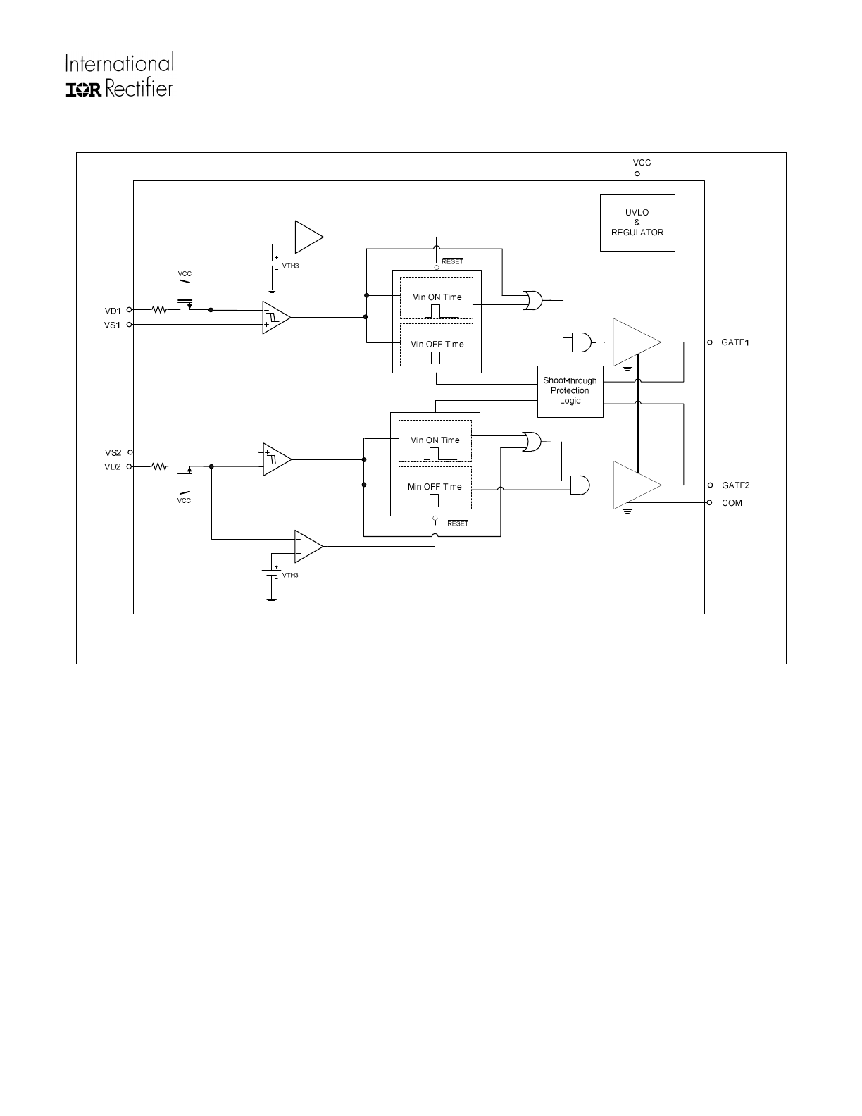
Functional Block Diagram
IR1168S
www.irf.com
© 2009 International Rectifier
9
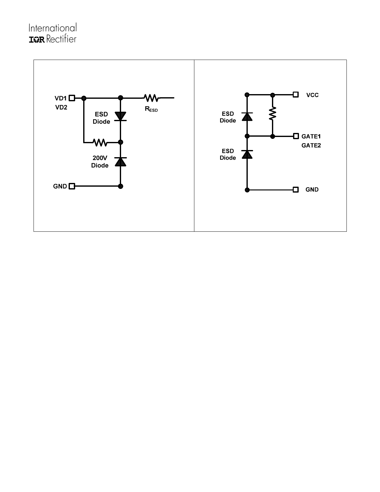
I/O Pin Equivalent Circuit Diagram
IR1168S
www.irf.com
© 2009 International Rectifier
10
Lead Definitions
PIN#
Symbol
Description
1
GATE1
Gate Drive Output 1
2
VCC
Supply Voltage
3
VS1
Sync FET 1 Source Voltage Sense
4
VD1
Sync FET 1 Drain Voltage Sense
5
VD2
Sync FET 2 Drain Voltage Sense
6
VS2
Sync FET 2 Source Voltage Sense
7
GND
Analog and Power Ground
8
GATE2
Gate Drive Output 2
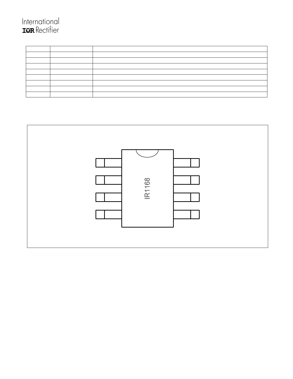
Lead Assignments
4
3
2
1
5
6
7
8
VD2
VD1
GND
GATE2
VCC
VS1
VS2
GATE1