
Datasheet TLE6280GP
1 2007-07-19
3-Phase Bridge Driver IC
Features
• Compatible to very low ohmic normal
level input N-Channel Mosfets
• Separate input for each MOSFET
• PWM frequency up to 30kHz
• Fulfills specification down to 9V
supply voltage
• Low EMC sensitivity and emission
• Separate Source connection for each MOSFET
• Adjustable dead time
• Adjustable dI/dt limitation
• Short circuit protection with adjustable current limitation
• Driver undervoltage warning
• Reverse polarity protection
• Disable function
• Input with TTL characteristics
• Error flag
• Thermal overload warning for driver IC
• Shoot through protection
• Shoot through option
• Integrated bootstrap diodes
• Green Product (RoHS compliant)
• AEC Qualified
Application
• Dedicated for 3-phase high current motor bridges in PWM control mode. This device fulfills requirements in
12V automotive applications
General Description
3-phase bridge driver IC for MOSFET power stages with multiple protection functions.
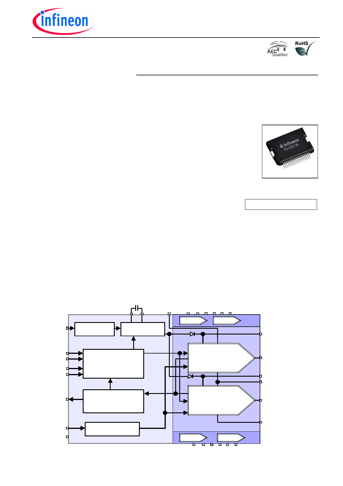
Block Diagram
Product Summary
Turn on current
I
Oxx(on)
0.9 A
Turn off current
I
Oxx(off)
0.85 A
Supply voltage range
V
Vs
8...20 V
Gate Voltage
V
GS
10
V
Temperature range
T
J
-40...+150 °C
PG-DSO36
Input Logic
- Shoot Through Option
- Charge Pump Control
- Programmable Dead Time
Error Logic
- Short Circuit Shut Down
- Under Voltage Warning
- Over Temperature Warning
HS Driver (Channel 2)
- Short Circuit Protection
- Undervoltage Detection
- DI/dt Control
LS Driver (Channel 2)
- Short Circuit Protection
- Undervoltage Detection
- DI/dt Control
Reverse Polarity
Protection
Voltage Regulator
Charge Pump
DI/dt Limitation
HS Driver 3
LS Driver 3
HS Driver 1
LS Driver 1
VDH
CH
CL
DIDT
ERR
DT
MFP
ILx
IHx
BH2
GH2
BL2
SH2
GL2
SL2
VS
BH1 GH1 SH1 BL1
GL1 SL1
BH3
GH3 SH3 BL3 GL3
SL3
GND
- Shoot Through Protection
Marking
TLE6280GP
Datasheet TLE6280GP
2 2007-07-19
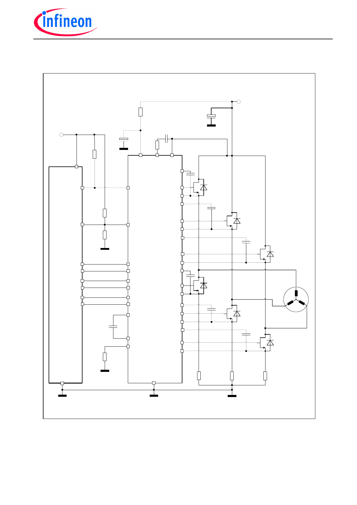
Application Block Diagram
Remark: This application diagram is one possible implementation of this driver IC. There is, e.g., the
possibility to link all three BLx pins and use only one capacitor.
SH1
V
S
=12V
C
1000µF
C
DI/DT
12nF
µC
GH1
R
Q
50 k
Ω
SH2
GH2
BH2
GL1
GL2
VS
V
CC
ERR
MFP
R
Q
82 k
Ω
IL1
IH1
C
BH1
220nF
C
BH2
220nF
C
VS
1µF
R
VS
10
Ω
GND
BH1
SL1
SH3
GH3
BH3
C
BH3
220nF
SL2
GL3
SL3
DI/DT
R
DI/DT
100
Ω
R
Q
20 k
Ω
V
5
=5V
IL2
IH2
IL3
IH3
GND
CH
CL
C
CP
1.5µF
VDH
DT
R
DT
50 k
Ω
BH3
C
BL3
220nF
BL2
C
BL2
220nF
BL1
C
BL1
220nF
TLE6280GP
P-GND
P-GND
Fig. 1 : Application circuit

Datasheet TLE6280GP
3 2007-07-19
Pin
Symbol Function
1;18;19:36 GND
Logic
Ground
8 VS
Voltage
supply
20
21
CL
CH
Charge pump - capacitor
9
11
13
IH1
IH2
IH3
Control inputs for high-side switches 1 to 3
(low active)
10
12
14
IL1
IL2
IL3
Control inputs for low-side switches 1 to 3
(high active)
15
MFP
Multi function pin:
a) Disable the complete device by V
MFP
<1V
b) Program pin for output voltage level under short
circuit condition (V
Gxx
–V
Sxx
= 2xV
MFP
)
c) Enable shoot through option by V
MFP
>4.5V
17
DT
Program pin for dead time
35
DIDT
Program pin dI/dt limitation
34
VDH
Sense pin for drain voltage of the high-side Mosfets
16
ERR
Error flag for driver supply under voltage, over-
temperature and short circuit (open drain output)
2
28
22
BH1
BH2
BH3
Bootstrap supply high-side switches 1 to 3
5
31
25
BL1
BL2
BL3
Backup capacitor connection low switches 1 to 3
3
29
23
GH1
GH2
GH3
Output to gate high-side switches 1 to 3
6
32
26
GL1
GL2
GL3
Output to gate low-side switches 1 to 3
4
30
24
SH1
SH2
SH3
Connection to source high-side switches 1 to 3
7
33
27
SL1
SL2
SL3
Connection to source low-side switches 1 to 3

Datasheet TLE6280GP
4 2007-07-19
Functional description
General
In the automotive sector there are more and more applications requiring high performance
motor drives, such as electro-hydraulic or electric power steering. In these applications
3-phase motors, synchronous and asynchronous, are used, combining high output perform-
ance, low space requirements and high reliability.
The TLE6280GP is a driver IC dedicated to control the 6 to 12 external Mosfets forming the
converter for high current 3 phase motor drives in the automotive sector. It incorporates fea-
tures like short circuit detection, diagnosis and high output performance and combines it with
typical automotive specific requirements like full functionality even at low battery voltages. Its
3 high-side and 3 low-side output stages are powerful enough to drive Mosfets with 250nC
gate charge with approx. 300ns fall and rise times.
Typical applications are cooling fan, water pump, electro-hydraulic and electric power steer-
ing. The TLE6280GP is designed for a 12V power net.
Use in 24V application is possible as well. Limiting factor could be the power dissipation.
This datasheet describes all functionality of this device. Additional application tips are given
in an application note available on the Internet.
Output stages
The 3 low-side and 3 high-side powerful push-pull output stages are all floating blocks, each
with its own Source pin. This allows the direct connection of the output stage to the Source
of each single Mosfet, allowing a perfect control of each Gate-Source voltage even when
200A are driven in the bridge with rise and fall times clearly below 1µs.
All 6 output stages have the same output power and, due to the use of the bootstrap princi-
ple, they can be switched all up to 30kHz.
Its output stages are powerful enough to drive Mosfets with 250nC gate charge with approx.
300ns fall and rise times, or even to run 12 such Mosfets with fall and rise times of approx.
600ns.
Maximum allowed power dissipation and the need to refresh the bootstrap capacitors with a
minimum refresh pulse limit the divice use for higher frequencies.
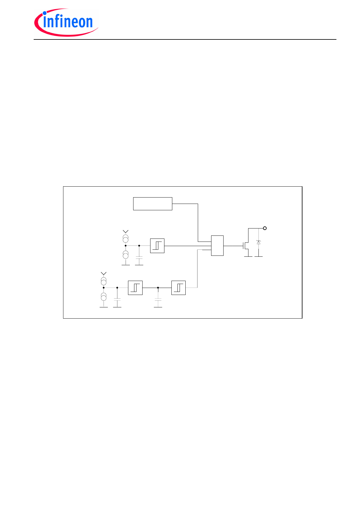
Fig. 2 shows the supply structure of TLE6280GP. The bootstrap capacitors are charged by
the charge pump capacitor C
CP
via the CH pin and diodes.
The exact value for this minimum refresh pulse is given by the RC time constant formed by
the impedance between the CH pin and Bxx pin, and the capacitor formed by the external
Mosfet (C
Mosfet
=Q
Gate-total
/ V
GS
). The size of the bootstrap capacitor has to be adapted to the
external Mosfet that the driver IC has to drive. Usually the bootstrap capacitor is about 10-20
times bigger than C
Mosfet
. External components, such as R-C networks, at the Vs Pin have to
be considered, too.
Operation at Vs<12V – integrated charge pump
The TLE6280GP provides a feature tailored to the requirements of 12V automotive applica-
tions. Often the operation of an application has to be assured even at 9V-supply voltage or
lower. Normally bridge driver ICs provide in such conditions clearly less than 9V to the Gate
of the external Mosfet, increasing its RDSon and associated the power dissipation.
The supply structure of the device is shown in fig.2. The TLE 6280GP has a built-in voltage
regulator with charge pump control to generate an internal supply voltage of 13V within a
supply voltage range of 8-40V. Operation below 8V is possible as well and will result in a re-
duced Gate voltage. The charge pump works with an external capacitor C
CP
connected be-
tween the CL and CH pins. It provides more than 13V at the CH pin and guarantees high
supply voltage for the bootstrap capacitors C
Bx
.
Datasheet TLE6280GP
5 2007-07-19
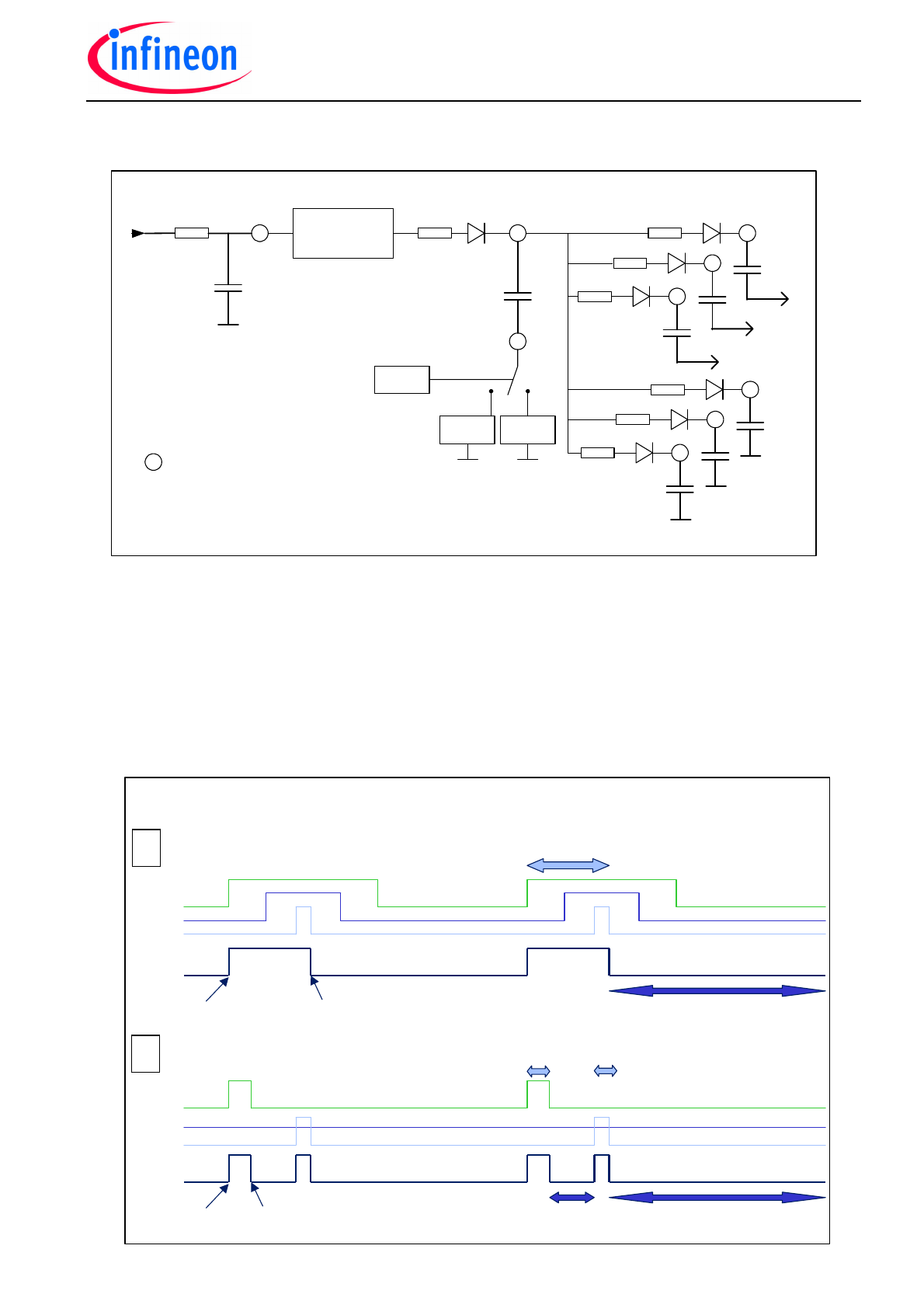
The Input Low-side pins ILx (see Fig. 3) trigger the charge pump. As soon as the first exter-
nal low-side Mosfet is switched on and the corresponding bootstrap capacitor is connected
to GND, the C
CP
is pushed to high and provides about 13V at the CH pin. C
CP
can now di-
rectly feed the low-side output stages and recharge the bootstrap capacitors connected to
GND.
As soon as the first of the 3 external low-side Mosfets is switched off, the C
CP
will be pulled
down to be re-charged.
This synchronous operation with the output stages has the benefit that the electromagnetic
emissions generated by the charge pump can be filtered by the same filter necessary to filter
the EME of the converter itself. At the same time it is assured that the high voltage at the CH
pin is available just in time to charge the high-side bootstrap.
Fig. 3: Trigger timing of charge pump caused by changing input signals
Vreg1 13V
+13 ... +8V
CH
CL
BH
1
BH
2
BH
3
BL
1
BL
2
BL
3
Vreg2=6V
Vreg3 =
Vreg1-8V
Triggered
by ILx
VS
C
CP
C
BH1
C
BL1
Phase A
Phase B
Phase C
= Pin
Bold line = external component
C
VS
from battery
R
VS
Fig. 2: Supply structure with external components (compare to Fig. 1)
IL1
IL2
Timing of charge pump - Examples
1
2
1. ILx high
1. ILx low
IL3
CH
Charge of bootstrap
capacitors
Charge of charge pump
capacitor
IL2
1. ILx high
1. ILx low
CH
Charge of bootstrap capacitors
IL1
IL3
Charge of charge pump capacitor

Datasheet TLE6280GP
6 2007-07-19
The size of the C
Bxx
and C
CP
capacitors depends upon the gate charge of the Mosfet.
(See “output stages”). C
CP
is usually 6 times larger then C
Bxx
.
Dead Time and Shoot through option.
In bridge applications it has to be assured that the external high-side and low-side Mosfets
are not “on” at the same time, such that the battery voltage is directly connected to GND.
This is usually assured by the integration of delays in a driver IC, generating a so-called
dead time between switching off the external Mosfet and switching on the other Mosfet of the
same half-bridge.
The dead times generated in the TLE6280GP are adjustable. The dead time generated by
the TLE6280GP can be varied from 100ns to 4µs by connecting an external resistor from the
DT pin to GND. The dead time has to be long enough to avoid a short between battery and
GND, while the dead time should be as short as possible to reduce extra power dissipation
in the external Mosfets.
In addition to this adjustable delay, the TLE6280GP provides a locking mechanism, prevent-
ing both external Mosfets of one half-bridge from being switched on at the same time. This
functionality is called shoot through protection.
If the command to switch on both high and low-side switches in the same half-bridge is given
at the input pins, the command will be ignored. (See dead time diagrams, fig. 6-8)
This shoot through protection can be deactivated by setting the MFP-pin to 5V.
Short circuit protection / current limitation
The TLE6280GP provides a short circuit protection for the external Mosfets, by monitoring
the Drain-Source voltage of the external Mosfets. As soon as this voltage is higher than the
short circuit detection limit, the Gate-Source voltage of this Mosfet will be limited to twice the
voltage at the MFP-Pin, providing a current limitation.
The short circuit detection level is dependent upon the voltage of the MFP pin as well (see
diagrams).
After a delay of about 11µs all external Mosfets will be switched off until the driver is reset by
the MFP pin. The error flag is set.
The Drain-Source voltage monitoring of the short circuit detection for certain external Mos-
fets is active as soon as the corresponding input is set to “on” and the dead time is expired.
This feature provides a 2-step switch-on behavior for each regular switching-on of a Mosfet.
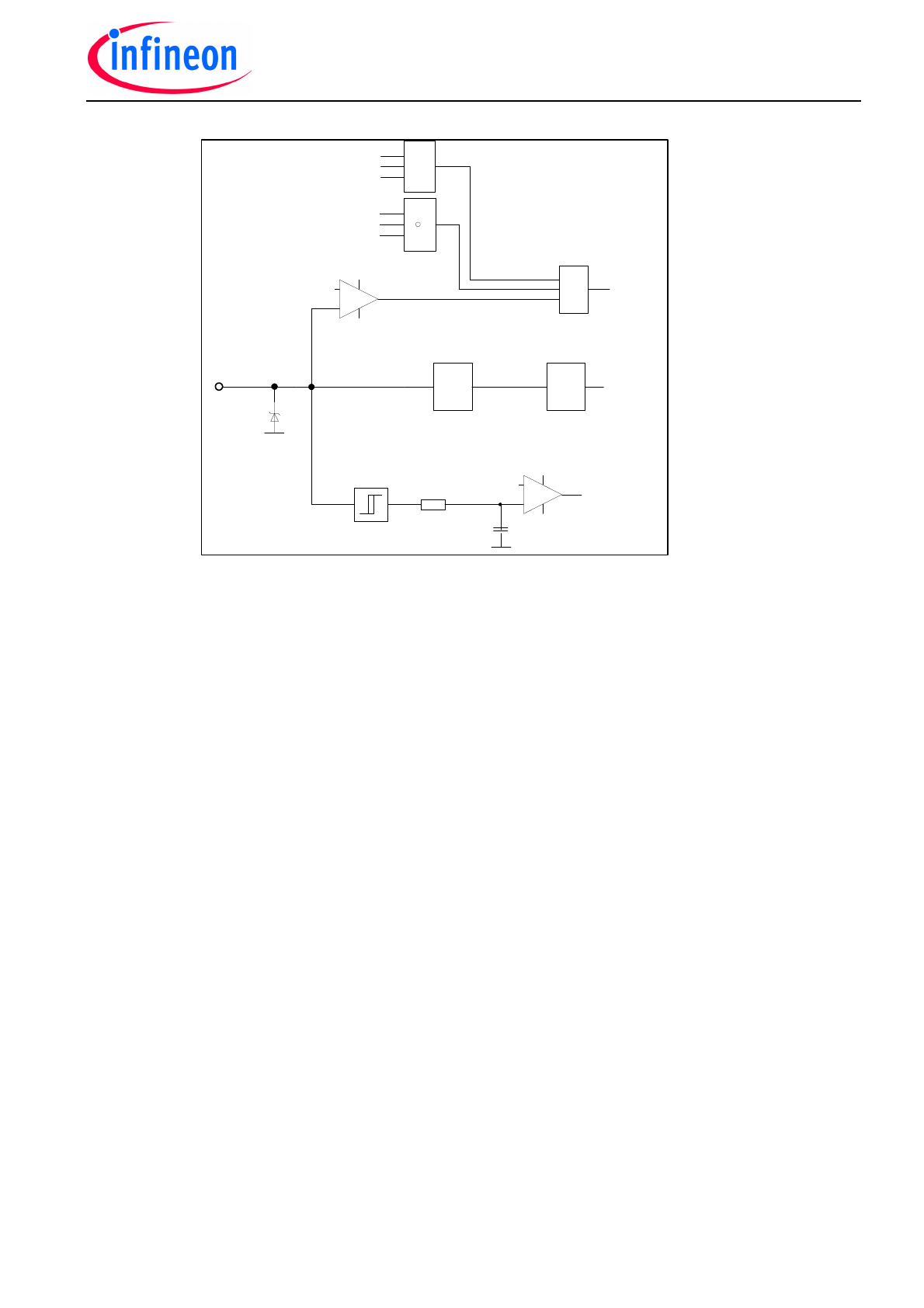
Description of MFP pin (Multi functional pin)
The MFP pin has multiple tasks:
1) Reset the device.
2) Adjust the short circuit detection level of the external Mosfet and define the gate voltage
limitation for current limitation in case of short circuit
3) Deactivate the shoot-through protection
Fig 4. shows the internal structure of the MFP pin.
Condition of MFP pin
Function
0 – 1.1V
Disable the driver. All external Mosfets will be actively
switched off
2.5 – 4.0 V
Adjustable short circuit detection level combined with adjust-
able gate voltage limitation for current limitation. Shoot-
through protection is active.
> 4.5V
Shoot-through protection deactivated.
Datasheet TLE6280GP
7 2007-07-19
Shoot through protection / option
As already mentioned, the device has a built-in shoot-through protection, to avoid a simulta-
neous activation of high- and low-side switch in one half-bridge.
In case there is a short circuit in the bridge, the driver will switch off all external Mosfets. If
there is still current flowing in the motor, it is possible for the user to override this shoot
through protection.
By setting the ILx to “high”, the IHx to “low” and MFP to a level above 4.5V, all external Mos-
fets will be turned on simultaneously to blow a well-dimensioned fuse. The application will be
finally disconnected in this way from battery, and thus guarantee that the motor does not ap-
ply any uncontrolled torque.
Undervoltage warning:
If the voltage of a bootstrap capacitor C
Bxx
reaches the undervoltage warning level the error
flag is set and will remain set until the voltage of the bootstrap capacitor has recovered.
The error signal can be seen as awarning that an undervoltage shut-down could occur soon,
and the user can take appropriate measures to avoid this. Such measures could be the
change of the duty cycle to a range of 10-90% or the ramp down of the motor.
Undervoltage shut down:
The TLE6280GP has an integrated undervoltage shut-down, to guarantee that the behavior
of the device is predictable in all voltage ranges.
If the voltage of a bootstrap capacitor C
Bxx
reaches the undervoltage shut-down level, the
Gate-Source voltage of the affected external Mosfet will be actively pulled to low. In this
situation the short circuit detection of this output stage is deactivated to avoid a complete
&
&
NAND
Vmfp x 2
MFP
Shoot
Through
80ns
1.45 /
1.7V
Gate
control
4.5V
IHx
ILx
Levelshifter
Dissable
=
Reset
Fig. 4: Block diagram of internal structure of MFP pin
Datasheet TLE6280GP
8 2007-07-19
shut down of the driver. This allows continued operation of the motor in case of undervoltage
shut-down for a short period of time.
As soon as the bootstrap voltage recovers, the output stage condition will be aligned to the
input patterns by the next changing input signal at the corresponding input pin.
Diagnosis
The ERR pin is an open collector output and has to be pulled up with external pull-up resis-
tors to 5V. In normal conditions the ERR signal is high. In case of an error the ERR pin is
pulled down. There are 3 different causes for an error signal:
1) Short circuit of an external Mosfet – all external Mosfets are switched off. The driver has
to be reset to start again.
2) Undervoltage warning: at least one of the external capacitors connected to Bxx pins has
a voltage below the warning level.
3) Over-temperature warning: The device works normally but is out of the maximum ratings.
Immediate actions have to be taken to reduce the thermal load. The error flag will be re-
moved when the driver reached temperatures below the over temperature warning level.
dI/dt control
In all high current PWM applications, transient overvoltages and electro-magnetic emmisions
are critical items. The dI/dt regulation of the TLE6280GP helps to reduce transient overvolt-
age as well as electro-magnetic emissions.
Each real bridge configuration has stray inductance in each half-bridge. When the Mosfets in
the bridge are switching and load current is flowing, the stray inductance together with the
dI/dt in the halfbridge causies transient overvoltages. These transient overvoltages can be
feed to the DIDT pin of the gate driver by a high pass filter. Voltages exceeding 2 to 5V or –2
to –5V at this pin will strongly reduce the gate current of the actually switched Mosfet, result-
ing in an increased switching time in the Miller plateau of the Mosfet, and reducing the
switching speed exactly and only in the critical area of the switching process. Through this
regulation over-voltages are reduced and a smoother dI/dt in the bridge is obtained.
For more detailed information please refer to application note.
Fig. 5: Block diagram of ERR functionality
OR
ERR
Iscp (VMFP)
3.3µA
0.3µA
10pF
Temperature
Sensor
I undervoltage
τ approx. 1µs

Datasheet TLE6280GP
9 2007-07-19
Estimation of power dissipation within the driver IC
The power dissipation within the driver IC is strongly dependent upon the use of the driver
and the external components. Nevertheless, a rough estimation of the worst case power dis-
sipation is possible.
Worst case calculation is:
P
D
= (Q
gate
*n*const* f
PWM
+ I
VS(open)
) * V
Vs
- P
RGate
With:
P
D
= Power dissipation in the driver IC
f
PWM
= Switching frequency
Q
gate
= Total gate charge of used MOSFET at 10V V
GS
n
= number of switched Mosfets
const
= constant considering some leakage current in the driver and the power dissipa-
tion caused by the charge pump (nominally = 2)
I
VS(open)
= Current consumption of driver without connected Mosfets during switching
V
VS
= Voltage at Vs
P
RGate
= Power dissipation in the external gate resistors
This value can be reduced dramatically by the use of external gate resistors.
Recommended start up procedure
To assure the driver to be active and functional, a special initialization procedure is required
whenever the gate drive is enabled (V
MFP
is changed from LO to HI). Every time the driver is
enabled, after 10
µs or later, positive-going transition signals at all ILx pins are required in or-
der to ensure proper start-up of the output driver. This procedure assures a proper wake up
the device and allowes to fill the bootstrap capacitors. Not filling the bootstrap capacitors
might lead to low Gate-Source voltages mainly in highside and can cause a short circuit de-
tection when the highside switches are activated. Not changing the ILx input signal after
enabling the device may cause the lowside outputs to stay in off conditions.

Datasheet TLE6280GP
10 2007-07-19
Maximum ratings
Parameter and Conditions Symbol
Values
Unit
at T
j
= -40 … +150 °C, unless otherwise specified
Supply voltage
1
V
S
-4 ... 45V
V
Operating temperature range
Storage temperature range
T
j
T
stg
-40 ...+150
-55 ...+150
°C
Max. voltage range at Ixx, MFP, DT; ERR
-0.3 ...+7
V
Max. voltage range at SLx
2
V
SLx
-7 ...+7
V
Max. voltage range at SHx
3
V
SHx
-7 ...+45
V
Max. voltage range at GLx
2
V
GLx
-7 ...+18
V
Max. voltage range at GHx
3
V
GHx
-7 ...+55
V
Max. voltage range at BHx
3
V
BHx
-0.3 ...+55
V
Max. voltage range at VDH
4
V
VDH
-4 ...+55
V
Max. voltage difference Bxx - Sxx
V
Bxx
-V
Sxx
-0.3 ...+15
V
Max. voltage difference Gxx - Sxx
V
Gxx
-V
Sxx
-0.3...+11
V
Max. voltage range at CL
V
CL
-0.3 ...+10
V
Max. voltage range at CH
V
CH
-0.3 ...+18
V
Max. voltage range at DIDT
V
DIDT
-7 ...+7
V
Power dissipation (DC) @ T
C
=125°C
P
tot
1.2
W
ESD voltage (Human Body Model)
JESD22-A114-B
@ all pins
@ all pins excluding Gxx
V
ESD
1
2
kV
DIN humidity category, DIN 40 040
E
IEC climatic category, DIN IEC 68-1
40/150/56
Jedec Level
3
Thermal resistance junction-case
R
thJC
≤5 K/W
1
With external resistor (
≥10 Ω ) and capacitor – see fig.1
2
The min value -7V is reduced to –(Vs - 0.5V) if Vs<7.5V
3
The min value -7V is reduced to –(V
BHx
-V
SHx
-1V) if bootstrap voltages <8V
4
The min value -4V is increased to –( V
BHx
- V
SHx
) if bootstrap voltages <4V