

RF & Protection Devices
Data Sheet
Revision 1.1, 2012-11-07
BFP420F
Low Noise Silicon Bipolar RF Transistor

Edition 2012-11-07
Published by
Infineon Technologies AG
81726 Munich, Germany
©
2013
Infineon Technologies AG
All Rights Reserved.
Legal Disclaimer
The information given in this document shall in no event be regarded as a guarantee of conditions or
characteristics. With respect to any examples or hints given herein, any typical values stated herein and/or any
information regarding the application of the device, Infineon Technologies hereby disclaims any and all warranties
and liabilities of any kind, including without limitation, warranties of non-infringement of intellectual property rights
of any third party.
Information
For further information on technology, delivery terms and conditions and prices, please contact the nearest
Infineon Technologies Office (
www.infineon.com
).
Warnings
Due to technical requirements, components may contain dangerous substances. For information on the types in
question, please contact the nearest Infineon Technologies Office.
Infineon Technologies components may be used in life-support devices or systems only with the express written
approval of Infineon Technologies, if a failure of such components can reasonably be expected to cause the failure
of that life-support device or system or to affect the safety or effectiveness of that device or system. Life support
devices or systems are intended to be implanted in the human body or to support and/or maintain and sustain
and/or protect human life. If they fail, it is reasonable to assume that the health of the user or other persons may
be endangered.

BFP420F
Data Sheet
3
Revision 1.1, 2012-11-07
Trademarks of Infineon Technologies AG
AURIX™, C166™, CanPAK™, CIPOS™, CIPURSE™, EconoPACK™, CoolMOS™, CoolSET™,
CORECONTROL™, CROSSAVE™, DAVE™, DI-POL™, EasyPIM™, EconoBRIDGE™, EconoDUAL™,
EconoPIM™, EconoPACK™, EiceDRIVER™, eupec™, FCOS™, HITFET™, HybridPACK™, I²RF™,
ISOFACE™, IsoPACK™, MIPAQ™, ModSTACK™, my-d™, NovalithIC™, OptiMOS™, ORIGA™,
POWERCODE™; PRIMARION™, PrimePACK™, PrimeSTACK™, PRO-SIL™, PROFET™, RASIC™,
ReverSave™, SatRIC™, SIEGET™, SINDRION™, SIPMOS™, SmartLEWIS™, SOLID FLASH™, TEMPFET™,
thinQ!™, TRENCHSTOP™, TriCore™.
Other Trademarks
Advance Design System™ (ADS) of Agilent Technologies, AMBA™, ARM™, MULTI-ICE™, KEIL™,
PRIMECELL™, REALVIEW™, THUMB™, µVision™ of ARM Limited, UK. AUTOSAR™ is licensed by AUTOSAR
development partnership. Bluetooth™ of Bluetooth SIG Inc. CAT-iq™ of DECT Forum. COLOSSUS™,
FirstGPS™ of Trimble Navigation Ltd. EMV™ of EMVCo, LLC (Visa Holdings Inc.). EPCOS™ of Epcos AG.
FLEXGO™ of Microsoft Corporation. FlexRay™ is licensed by FlexRay Consortium. HYPERTERMINAL™ of
Hilgraeve Incorporated. IEC™ of Commission Electrotechnique Internationale. IrDA™ of Infrared Data
Association Corporation. ISO™ of INTERNATIONAL ORGANIZATION FOR STANDARDIZATION. MATLAB™ of
MathWorks, Inc. MAXIM™ of Maxim Integrated Products, Inc. MICROTEC™, NUCLEUS™ of Mentor Graphics
Corporation. MIPI™ of MIPI Alliance, Inc. MIPS™ of MIPS Technologies, Inc., USA. muRata™ of MURATA
MANUFACTURING CO., MICROWAVE OFFICE™ (MWO) of Applied Wave Research Inc., OmniVision™ of
OmniVision Technologies, Inc. Openwave™ Openwave Systems Inc. RED HAT™ Red Hat, Inc. RFMD™ RF
Micro Devices, Inc. SIRIUS™ of Sirius Satellite Radio Inc. SOLARIS™ of Sun Microsystems, Inc. SPANSION™
of Spansion LLC Ltd. Symbian™ of Symbian Software Limited. TAIYO YUDEN™ of Taiyo Yuden Co.
TEAKLITE™ of CEVA, Inc. TEKTRONIX™ of Tektronix Inc. TOKO™ of TOKO KABUSHIKI KAISHA TA. UNIX™
of X/Open Company Limited. VERILOG™, PALLADIUM™ of Cadence Design Systems, Inc. VLYNQ™ of Texas
Instruments Incorporated. VXWORKS™, WIND RIVER™ of WIND RIVER SYSTEMS, INC. ZETEX™ of Diodes
Zetex Limited.
Last Trademarks Update 2011-11-11
BFP420F, Low Noise Silicon Bipolar RF Transistor
Revision History: 2012-11-07, Revision 1.1
Previous Revision: Rev. 1.0
Page
Subjects (major changes since last revision)
This datasheet replaces the revision from 2012-01-30.
The product itself has not been changed and the device characteristics remain unchanged.
Only the product description and information available in the datasheet has been expanded and
updated.

BFP420F
Table of Contents
Data Sheet
4
Revision 1.1, 2012-11-07
Table of Contents
. . . . . . . . . . . . . . . . . . . . . . . . . . . . . . . . . . . . . . . . . . . . . . . . . . . . . . . . . . . . . . . . 4
List of Figures
. . . . . . . . . . . . . . . . . . . . . . . . . . . . . . . . . . . . . . . . . . . . . . . . . . . . . . . . . . . . . . . . . . . 5
List of Tables
. . . . . . . . . . . . . . . . . . . . . . . . . . . . . . . . . . . . . . . . . . . . . . . . . . . . . . . . . . . . . . . . . . . . 6
1
Product Brief
. . . . . . . . . . . . . . . . . . . . . . . . . . . . . . . . . . . . . . . . . . . . . . . . . . . . . . . . . . . . . . . . . . . . 7
2
Features
. . . . . . . . . . . . . . . . . . . . . . . . . . . . . . . . . . . . . . . . . . . . . . . . . . . . . . . . . . . . . . . . . . . . . . . . 8
3
Maximum Ratings
. . . . . . . . . . . . . . . . . . . . . . . . . . . . . . . . . . . . . . . . . . . . . . . . . . . . . . . . . . . . . . . . 9
4
Thermal Characteristics
. . . . . . . . . . . . . . . . . . . . . . . . . . . . . . . . . . . . . . . . . . . . . . . . . . . . . . . . . . 10
5
Electrical Characteristics
. . . . . . . . . . . . . . . . . . . . . . . . . . . . . . . . . . . . . . . . . . . . . . . . . . . . . . . . . 11
5.1
DC Characteristics . . . . . . . . . . . . . . . . . . . . . . . . . . . . . . . . . . . . . . . . . . . . . . . . . . . . . . . . . . . . . . . 11
5.2
General AC Characteristics . . . . . . . . . . . . . . . . . . . . . . . . . . . . . . . . . . . . . . . . . . . . . . . . . . . . . . . . 11
5.3
Frequency Dependent AC Characteristics . . . . . . . . . . . . . . . . . . . . . . . . . . . . . . . . . . . . . . . . . . . . . 12
5.4
Characteristic DC Diagrams . . . . . . . . . . . . . . . . . . . . . . . . . . . . . . . . . . . . . . . . . . . . . . . . . . . . . . . . 18
5.5
Characteristic AC Diagrams . . . . . . . . . . . . . . . . . . . . . . . . . . . . . . . . . . . . . . . . . . . . . . . . . . . . . . . . 21
6
Simulation Data
. . . . . . . . . . . . . . . . . . . . . . . . . . . . . . . . . . . . . . . . . . . . . . . . . . . . . . . . . . . . . . . . . 28
7
Package Information TSFP-4-1
. . . . . . . . . . . . . . . . . . . . . . . . . . . . . . . . . . . . . . . . . . . . . . . . . . . . 29
Table of Contents

BFP420F
List of Figures
Data Sheet
5
Revision 1.1, 2012-11-07
Figure 4-1
Total Power Dissipation
P
tot
=
f
(
T
s
) . . . . . . . . . . . . . . . . . . . . . . . . . . . . . . . . . . . . . . . . . . . . . . . . 10
Figure 5-1
BFP420F Testing Circuit. . . . . . . . . . . . . . . . . . . . . . . . . . . . . . . . . . . . . . . . . . . . . . . . . . . . . . . . . 12
Figure 5-2
Collector Current vs. Collector Emitter Voltage
I
C =
f
(V
CE
),
I
B
= Parameter in
μA . . . . . . . . . . . . 18
Figure 5-3
DC Current Gain
h
FE
=
f
(
I
C
),
V
CE
= 3 V . . . . . . . . . . . . . . . . . . . . . . . . . . . . . . . . . . . . . . . . . . . . . 18
Figure 5-4
Collector Current vs. Base Emitter Voltage
I
C
=
f
(
V
BE
),
V
CE
= 3 V. . . . . . . . . . . . . . . . . . . . . . . . . 19
Figure 5-5
Base Current vs. Base Emitter Forward Voltage
I
B
=
f
(
V
BE
),
V
CE
= 3 V . . . . . . . . . . . . . . . . . . . . 19
Figure 5-6
Base Current vs. Base Emitter Reverse Voltage
I
B
=
f
(
V
EB
),
V
CE
= 3 V . . . . . . . . . . . . . . . . . . . . 20
Figure 5-7
Collector Emitter Breakdown Voltage
V
CER
=
f
(
R
BE
),
I
C
= 1 mA. . . . . . . . . . . . . . . . . . . . . . . . . . . 20
Figure 5-8
Transition Frequency
f
T
=
f
(
I
C
),
f
= 2 GHz,
V
CE
= Parameter in V . . . . . . . . . . . . . . . . . . . . . . . . . 21
Figure 5-9
3rd Order Intercept Point
OIP
3
=
f
(
I
C
),
Z
S
=
Z
L
= 50 Ω,
V
CE
,
f
= Parameters . . . . . . . . . . . . . . . . . 21
Figure 5-10 3rd Order Intercept Point at output
OIP
3
[dBm]=
f
(
I
C
,
V
CE
),
Z
S
=
Z
L
= 50 Ω,
f
= 1900 MHz . . . . . . 22
Figure 5-11 Compression Point at output
OP
1dB
[dBm]=
f
(
I
C
,
V
CE
),
Z
S
=
Z
L
= 50 Ω,
f
= 1900 MHz . . . . . . . . . . 22
Figure 5-12 Collector Base Capacitance
C
CB
= f
(
V
CB
),
f
= 1 MHz . . . . . . . . . . . . . . . . . . . . . . . . . . . . . . . . . . 23
Figure 5-13 Gain
G
ma
,
G
ms
, I
S
21
I² =
f
(
f
),
V
CE
= 3 V,
I
C
= 15 mA . . . . . . . . . . . . . . . . . . . . . . . . . . . . . . . . . . . . 23
Figure 5-14 Maximum Power Gain
G
max
=
f
(
I
C
),
V
CE
= 3 V,
f
= Parameter in GHz . . . . . . . . . . . . . . . . . . . . . . 24
Figure 5-15 Maximum Power Gain
G
max
=
f
(
V
CE
),
I
C
= 15 mA,
f
= Parameter in GHz . . . . . . . . . . . . . . . . . . . 24
Figure 5-16 Input Matching
S
11
=
f
(
f
),
V
CE
= 3 V,
I
C
= 4 / 15 / 40 mA . . . . . . . . . . . . . . . . . . . . . . . . . . . . . . . . 25
Figure 5-17 Source Impedance for Minimum Noise Figure
Z
opt
=
f
(
f
),
V
CE
= 3 V,
I
C
= 4 / 15 mA . . . . . . . . . . . 25
Figure 5-18 Output Matching
S
22
=
f
(
f
),
V
CE
= 3 V,
I
C
= 4 / 15 / 40 mA . . . . . . . . . . . . . . . . . . . . . . . . . . . . . . . 26
Figure 5-19 Noise Figure
NF
min
=
f
(f
),
V
CE
= 3 V,
I
C
= 4 / 16 mA,
Z
S
=
Z
opt
. . . . . . . . . . . . . . . . . . . . . . . . . . . 26
Figure 5-20 Noise Figure
NF
min
=
f
(
I
C
),
V
CE
= 3 V,
Z
S
=
Z
opt
,
f
= Parameter in GHz. . . . . . . . . . . . . . . . . . . . . 27
Figure 5-21 Noise Figure
NF
50
=
f
(
I
C
),
V
CE
= 3 V,
Z
S
= 50 Ω,
f
= Parameter in GHz . . . . . . . . . . . . . . . . . . . . 27
Figure 7-1
Package Outline . . . . . . . . . . . . . . . . . . . . . . . . . . . . . . . . . . . . . . . . . . . . . . . . . . . . . . . . . . . . . . . 29
Figure 7-2
Package Footprint. . . . . . . . . . . . . . . . . . . . . . . . . . . . . . . . . . . . . . . . . . . . . . . . . . . . . . . . . . . . . . 29
Figure 7-3
Marking Description (Marking BFP420F: AMs) . . . . . . . . . . . . . . . . . . . . . . . . . . . . . . . . . . . . . . . 29
Figure 7-4
Tape Dimensions . . . . . . . . . . . . . . . . . . . . . . . . . . . . . . . . . . . . . . . . . . . . . . . . . . . . . . . . . . . . . . 29
List of Figures

BFP420F
List of Tables
Data Sheet
6
Revision 1.1, 2012-11-07
Table 3-1
Maximum Ratings at
T
A
= 25 °C (unless otherwise specified) . . . . . . . . . . . . . . . . . . . . . . . . . . . . . 9
Table 4-1
Thermal Resistance . . . . . . . . . . . . . . . . . . . . . . . . . . . . . . . . . . . . . . . . . . . . . . . . . . . . . . . . . . . . 10
Table 5-1
DC Characteristics at
T
A
= 25 °C . . . . . . . . . . . . . . . . . . . . . . . . . . . . . . . . . . . . . . . . . . . . . . . . . 11
Table 5-2
General AC Characteristics at
T
A
= 25 °C . . . . . . . . . . . . . . . . . . . . . . . . . . . . . . . . . . . . . . . . . . . 11
Table 5-3
AC Characteristics,
f
= 150 MHz . . . . . . . . . . . . . . . . . . . . . . . . . . . . . . . . . . . . . . . . . . . . . . . . . . 12
Table 5-4
AC Characteristics,
f
= 450 MHz . . . . . . . . . . . . . . . . . . . . . . . . . . . . . . . . . . . . . . . . . . . . . . . . . . 13
Table 5-5
AC Characteristics,
f
= 900 MHz . . . . . . . . . . . . . . . . . . . . . . . . . . . . . . . . . . . . . . . . . . . . . . . . . . 13
Table 5-6
AC Characteristics,
f
= 1500 MHz . . . . . . . . . . . . . . . . . . . . . . . . . . . . . . . . . . . . . . . . . . . . . . . . . 14
Table 5-7
AC Characteristics,
f
= 1900 MHz . . . . . . . . . . . . . . . . . . . . . . . . . . . . . . . . . . . . . . . . . . . . . . . . . 15
Table 5-8
AC Characteristics,
f
= 2400 MHz . . . . . . . . . . . . . . . . . . . . . . . . . . . . . . . . . . . . . . . . . . . . . . . . . 15
Table 5-9
AC Characteristics,
f
= 3500 MHz . . . . . . . . . . . . . . . . . . . . . . . . . . . . . . . . . . . . . . . . . . . . . . . . . 16
Table 5-10 AC Characteristics,
f
= 5500 MHz . . . . . . . . . . . . . . . . . . . . . . . . . . . . . . . . . . . . . . . . . . . . . . . . . 17
List of Tables

BFP420F
Product Brief
Data Sheet
7
Revision 1.1, 2012-11-07
1
Product Brief
The BFP420F is a low noise wideband NPN bipolar RF transistor. The collector design supports voltages up to
V
CEO
= 4.5 V and currents up to
I
C
= 60 mA. The device is especially suited for mobile applications in which low
power consumption is a key requirement. The typical transition frequency is approximately 25 GHz, hence the
device offers high power gain at frequencies up to 4.5 GHz in amplifier applications. The device is housed in a thin
small flat plastic package with visible leads.
BFP420F
Features
Data Sheet
8
Revision 1.1, 2012-11-07
2
Features
Applications
As Low Noise Amplifier (LNA) in
•
Satellite communication systems: Navigation systems (GPS, Glonass), satellite radio (SDARs, DAB)
•
Multimedia applications such as mobile/portable TV, CATV, FM Radio
•
ISM applications like RKE, AMR and Zigbee, as well as for emerging wireless applications
As discrete active mixer in RF Frontends
As active device in discrete oscillators
Attention: ESD (Electrostatic discharge) sensitive device, observe handling precautions
•
General purpose low noise NPN bipolar RF transistor
•
Based on Infineon´s reliable very high volume 25 GHz
silicon bipolar technology
•
0.95 dB minimum noise figure typical at 900 MHz, 3 V, 4 mA
•
16.5 dB maximum gain (
G
ma
) typical at 2.4 GHz, 3 V, 15 mA
•
28 dBm
OIP
3
typical at 2.4 GHz, 4 V, 40 mA
•
16.5 dBm
OP
1dB
typical at 2.4 GHz, 4 V, 40 mA
•
Popular in discrete oscillators
•
Thin, small, flat, Pb-free (RoHS compliant) and Halogen-free
package with visible leads
•
Qualification report according to AEC-Q101 available
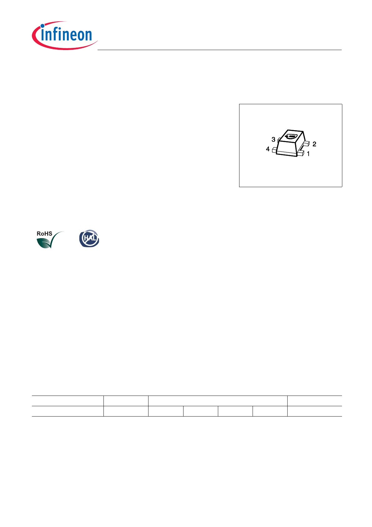
Product Name
Package
Pin Configuration
Marking
BFP420F
TSFP-4-1
1 = B
2 = E
3 = C
4 = E
AMs

BFP420F
Maximum Ratings
Data Sheet
9
Revision 1.1, 2012-11-07
3
Maximum Ratings
Attention: Stresses above the max. values listed here may cause permanent damage to the device.
Exposure to absolute maximum rating conditions for extended periods may affect device
reliability. Maximum ratings are absolute ratings; exceeding only one of these values may
cause irreversible damage to the integrated circuit.
Table 3-1
Maximum Ratings at
T
A
= 25 °C (unless otherwise specified)
Parameter
Symbol
Values
Unit
Note / Test Condition
Min.
Max.
Collector emitter voltage
V
CEO
–
–
4.5
4.1
V
Open base
T
A
= 25 °C
T
A
= -55 °C
Collector base voltage
V
CBO
–
15
V
Open emitter
Collector emitter voltage
V
CES
–
15
V
E-B short circuited
Emitter base voltage
V
EBO
–
1.5
V
Open collector
Base current
I
B
–
9
mA
–
Collector current
I
C
–
60
mA
–
Total power dissipation
1)
1)
T
S
is the soldering point temperature.
T
S
is measured on the emitter lead at the soldering point of the pcb.
P
tot
–
210
mW
T
S
≤ 100 °C
Junction temperature
T
J
–
150
°C
–
Storage temperature
T
Stg
-55
150
°C
–
BFP420F
Thermal Characteristics
Data Sheet
10
Revision 1.1, 2012-11-07
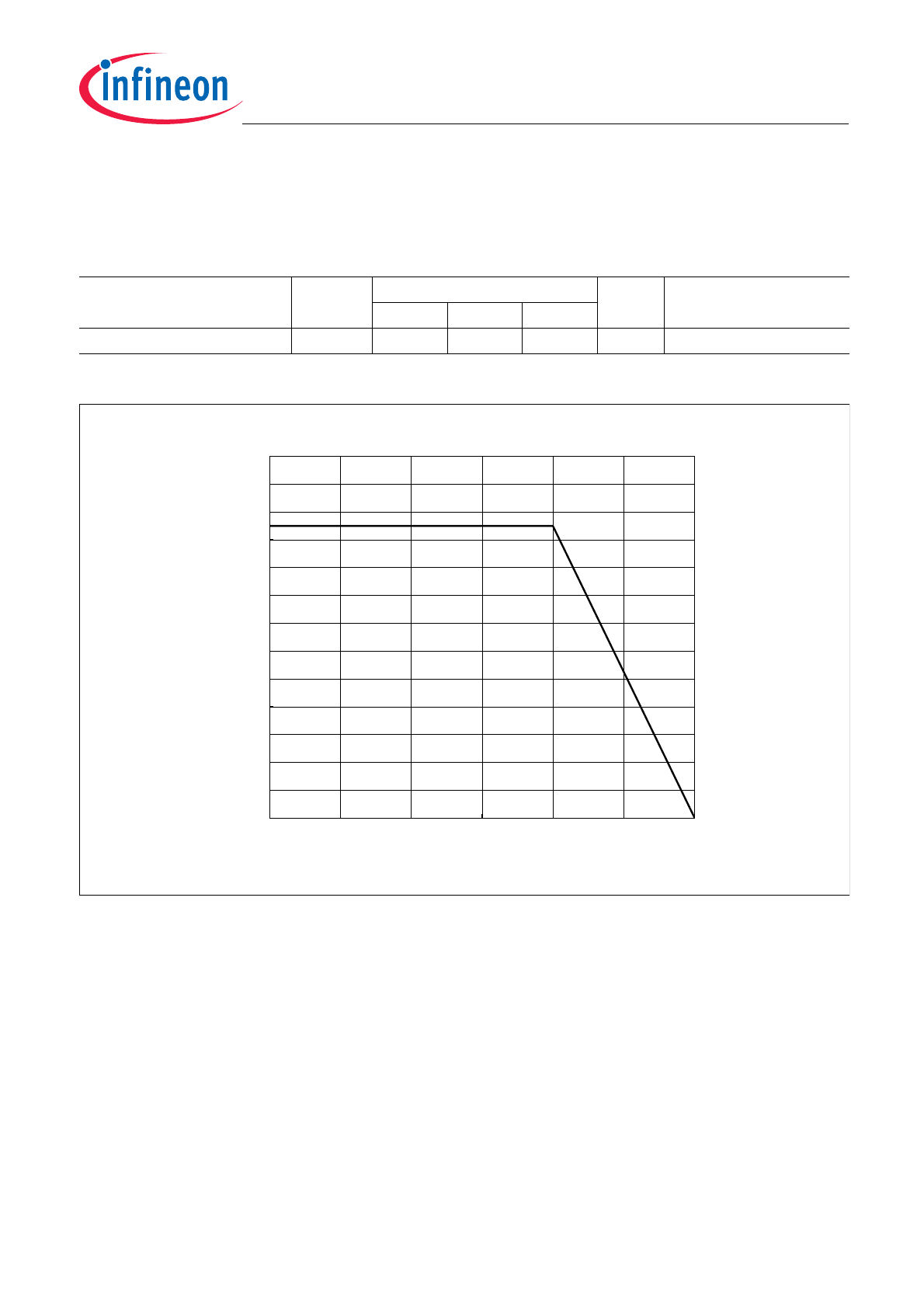
4
Thermal Characteristics
Figure 4-1 Total Power Dissipation
P
tot
=
f
(
T
s
)
Table 4-1
Thermal Resistance
Parameter
Symbol
Values
Unit
Note / Test Condition
Min.
Typ.
Max.
Junction - soldering point
1)
1)For the definition of R
thJS
please refer to Application Note AN077 (Thermal Resistance Calculation)
R
thJS
–
240
–
K/W
–
0
25
50
75
100
125
150
0
20
40
60
80
100
120
140
160
180
200
220
240
260
T
S
[°C]
P
tot
[mW]