
www.irf.com
© 2008 International Rectifier
1
IRS20957S
Protected Digital Audio Driver
Features
Floating PWM input enables easy half bridge
implementation
Programmable bidirectional over-current protection with
self-reset function
Programmable preset dead-time for improved THD
performances
High noise immunity
100V ratings deliver up to 500W in output power
3.3 V/ 5 V logic compatible input
Operates up to 800kHz
Typical Applications
Home theatre systems
Mini component stereo systems
Powered speaker systems
General purpose audio power amplifiers
Product Summary
Topology
Half-Bridge
V
OFFSET (max)
+/- 100 V
I
O+
& I
O-
(typical)
1.0 A & 1.2 A
Selectable deadtime
15/25/35/80ns
Ton & toff (typical)
95ns & 80ns
OC protection delay
500ns (max)
Shutdown
propagation delay
250ns (max)
Package
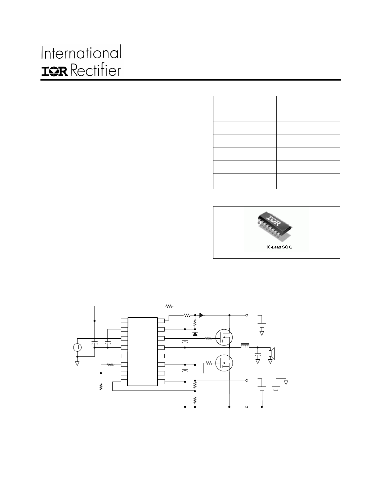
Typical Connection Diagram
IRS20957S
12V
-B
Vcc
Speaker
+B
PWM
VDD
CSD
IN
OCSET
COM
VSS
LO
VCC
VREF
HO
VS
NC
CSH
VB
DT
2
16
1
4
3
5
6
7
8
15
14
13
12
11
10
9
NC
Note: Please refer to Lead Assignments for correct pin configuration. This diagram shows
electrical connections only.
Sept 19, 2016
Datasheet No
– PD
IRS20957S
www.irf.com
© 2008 International Rectifier
2
Table of Contents
Page
Description
3
Qualification Information
4
Absolute Maximum Ratings
5
Recommended Operating Conditions
6
Electrical Characteristics
7
Functional Block Diagram
9
Input/Output Pin Equivalent Circuit Diagram
10
Lead Definitions
11
Lead Assignments
11
Waveform definitions
12
Application information and additional information
12
Package Details
13
Tape and Reel Details
14
Part Marking Information
15
Ordering Information
16

IRS20957S
www.irf.com
© 2008 International Rectifier
3
Description
The IRS20957S is a high voltage, high speed MOSFET driver with a floating PWM input designed for Class
D audio amplifier applications.
Bi-directional current sensing detects over current conditions during positive and negative load currents
without any external shunt resistors. A built-in protection control block provides a secure protection
sequence against over-current conditions and a programmable reset timer.
The internal dead-time generation block enables accurate gate switching and optimum dead-time setting
for better audio performance, such as lower THD and lower audio noise floor.
IRS20957S
www.irf.com
© 2008 International Rectifier
4
Qualification Information
†
Qualification Level
Industrial
††
Comments: This family of ICs has passed JEDEC’s
Industrial qualification. IR’s Consumer qualification level is
granted by extension of the higher Industrial level.
Moisture Sensitivity Level
SOIC16N
MSL2
†††
260°C
(per IPC/JEDEC J-STD-020)
ESD
Machine Model
Class B
(per JEDEC standard EIA/JESD22-A115)
Human Body Model
Class 2
(per EIA/JEDEC standard JESD22-A114)
IC Latch-Up Test
Class I , Level A
(per JESD78)
RoHS Compliant
Yes
†
Qualification standards can be found at International Rectifier’s web site
http://www.irf.com/
†† Higher qualification ratings may be available should the user have such requirements. Please
contact your International Rectifier sales representative for further information.
††† Higher MSL ratings may be available for the specific package types listed here. Please contact
your International Rectifier sales representative for further information.
IRS20957S
www.irf.com
© 2008 International Rectifier
5
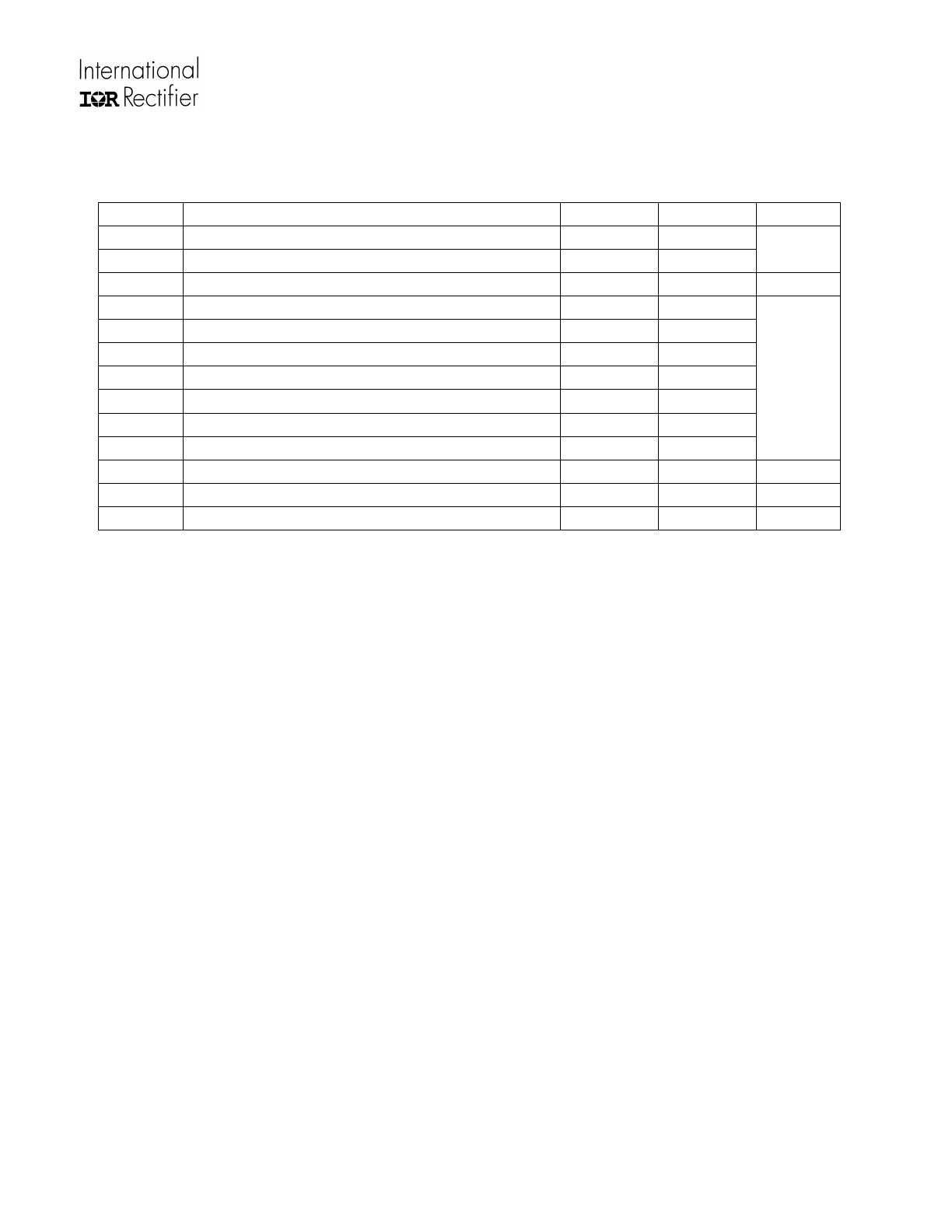
Absolute Maximum Ratings
Absolute Maximum Ratings indicate sustained limits beyond which damage to the device may occur. All
voltage parameters are absolute voltages referenced to COM; all currents are defined positive into any
lead. The Thermal Resistance and Power Dissipation ratings are measured under board mounted and still
air conditions.
Symbol
Definition
Min.
Max.
Units
V
B
High side floating supply voltage
-0.3
215
V
V
S
High side floating supply voltage
†
V
B
-15
V
B
+0.3
V
HO
High side floating output voltage
Vs-0.3
V
B
+0.3
V
CSH
CSH pin input voltage
Vs-0.3
V
B
+0.3
V
CC
Low side fixed supply voltage
†
-0.3
20
V
LO
Low side output voltage
-0.3
V
CC
+0.3
V
DD
Floating input supply voltage
-0.3
210
V
SS
Floating input supply voltage
†
(See I
DDZ
)
V
DD
+0.3
V
IN
PWM input voltage
V
SS
-0.3
V
DD
+0.3
V
CSD
CSD pin input voltage
V
SS
-0.3
V
DD
+0.3
V
DT
DT pin input voltage
-0.3
V
CC
+0.3
V
OCSET
OCSET
pin input voltage
-0.3
V
CC
+0.3
V
REF
VREF pin voltage
-0.3
V
CC
+0.3
I
DDZ
Floating input supply zener clamp current
†
-
10
mA
I
CCZ
Low side supply zener clamp current
†
-
10
I
BSZ
Floating supply zener clamp current
†
-
10
I
OREF
Reference output current
-
5
d V
S
/dt
Allowable V
S
voltage slew rate
-
50
V/ns
d V
SS
/dt
Allowable V
SS
voltage slew rate
††
-
50
d V
SS
/dt
Allowable V
SS
voltage slew rate upon power-up
†††
-
50
V/ms
Pd
Maximum power dissipation
-
1.0
W
Rth
JA
Thermal resistance, Junction to ambient
-
115
C/W
T
J
Junction Temperature
-
150
C
T
S
Storage Temperature
-55
150
T
L
Lead temperature (Soldering, 10 seconds)
-
300
†
V
DD
- V
SS
, V
CC
-COM and V
B
- V
S
contain internal shunt zener diodes. Please note that the
voltage ratings of these can be limited by the clamping current.
††
For the rising and falling edges of step signal of 10V. Vss=15V to 200V.
††† Vss ramps up from 0V to 200V.
IRS20957S
www.irf.com
© 2008 International Rectifier
6
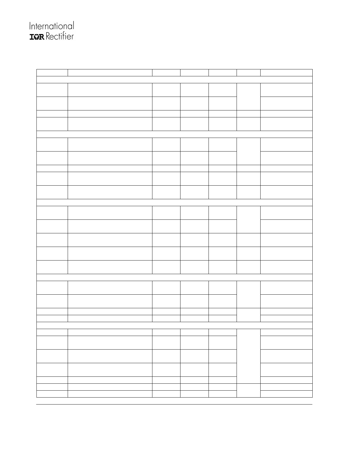
Recommended Operating Conditions
For proper operation, the device should be used within the recommended conditions below. The Vs and
COM offset ratings are tested with supplies biased at I
DD
=5mA, V
CC
=12V and V
B
-V
S
=12V.
Symbol
Definition
Min.
Max.
Units
V
B
High side floating supply absolute voltage
Vs+10
Vs+14
V
V
S
High side floating supply offset voltage
†
200
I
DDZ
Floating input supply zener clamp current
1
5
mA
V
SS
Floating input supply absolute voltage
0
100
V
V
HO
High side floating output voltage
Vs
V
B
V
CC
Low side fixed supply voltage
10
15
V
LO
Low side output voltage
0
V
CC
V
IN
PWM input voltage
V
SS
V
DD
V
CSD
CSD pin input voltage
V
SS
V
DD
V
DT
DT pin input voltage
0
V
CC
I
OREF
Reference output current to COM
†
0.3
0.8
mA
V
OCSET
OCSET
pin input voltage
0.5
5
V
T
A
Ambient Temperature
-40
125
C
†
Logic operational for Vs equal to
–5V to +200V. Logic state held for Vs equal to –5V to –V
BS
.
††
Nominal voltage for V
REF
is 5V. I
OREF
of 0.3
– 0.8mA dictates total external resistor value on
VREF to be 6.3k to 16.7k Ω.
IRS20957S
www.irf.com
© 2008 International Rectifier
7
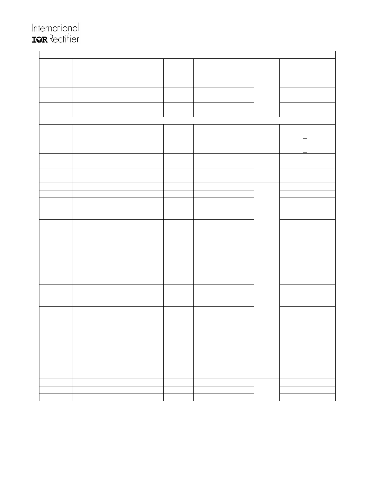
Electrical Characteristics
V
CC
,V
BS
= 12 V, I
DD
=5mA, V
SS
=20V, V
S
=0V,C
L
=1nF and T
A
=25
C unless otherwise specified.
Symbol
Description
Min
Typ
Max
Units
Test Conditions
Low Side Supply
UV
CC+
V
CC
supply UVLO positive
threshold
8.4
8.9
9.4
V
UV
CC-
V
CC
supply UVLO negative
threshold
8.2
8.7
9.2
I
QCC
Low side quiescent current
-
-
3
mA
V
DT
= V
CC
V
CLAMPL
Low side zener diode clamp
voltage
19.6
20.4
21.6
V
I
CC
=5mA
High Side Floating Supply
UV
BS+
High side well UVLO positive
threshold
8.0
8.5
9.0
V
UV
BS-
High side well UVLO negative
threshold
7.8
8.3
8.8
I
QBS
High side quiescent current
-
-
1
mA
I
LKH
High to Low side leakage
current
-
-
50
µA
V
B
=V
S
=200V
V
CLAMPH
High side zener diode clamp
voltage
14.7
15.3
16.2
V
I
BS
=5mA
Floating Input Supply
UV
DD+
V
DD
, V
SS
floating supply
UVLO positive threshold
8.2
8.7
9.2
V
V
SS
=0V
UV
DD-
V
DD
, V
SS
floating supply
UVLO negative threshold
7.7
8.2
8.7
V
SS
=0V
I
QDD
Floating Input quiescent
current
-
-
1
mA
V
DD
=9.5V +Vss
V
CLAMPM
Floating Input zener diode
clamp voltage
9.8
10.2
10.8
V
I
DD
=5mA
I
LKM
Floating input side to Low side
leakage current
-
-
50
µA
V
DD
=V
SS
=200V
Floating PWM Input
V
IH
Logic high input threshold
voltage
2.3
1.9
-
V
V
IL
Logic low input threshold
voltage
-
1.9
1.5
I
IN+
Logic “1” input bias current
-
-
40
µA
V
IN
=3.3V
I
IN-
Logic “0” input bias current
-
-
1
V
IN
= V
SS
Protection
V
REF
Reference output voltage
4.8
5.1
5.4
V
I
OREF
=0.5mA
Vth
OCL
Low side OC threshold in Vs
1.1
1.2
1.3
OCSET=1.2V,
Figure 3
Vth
OCH
High side OC threshold in
V
CSH
1.1+ Vs
1.2+ Vs
1.3+ Vs
Vs=200V,
Figure 4
Vth1
CSD pin shutdown release
threshold
0.62xV
DD
0.70xV
DD
0.78xV
DD
V
SS
=0V
Vth2
CSD pin self reset threshold
0.26xV
DD
0.30xV
DD
0.34xV
DD
V
SS
=0V
I
CSD+
CSD pin discharge current
70
100
130
µA
V
SD
= V
SS
+5V
I
CSD-
CSD pin charge current
70
100
130
V
SD
= V
SS
+5V
IRS20957S
www.irf.com
© 2008 International Rectifier
8
Protection (continued)
Symbol
Description
Min
Typ
Max
Units
Test Conditions
t
SD
Shutdown propagation delay
from V
CSD
> V
SS
+ Vth
OCH
to
Shutdown
-
-
250
ns
Figure 2
t
OCH
Propagation delay time from
V
CSH
> Vth
OCH
to Shutdown
-
-
500
Figure 4
t
OCL
Propagation delay time from
Vs> Vth
OCL
to Shutdown
-
-
500
Figure 3
Gate Driver
Io+
Output high short circuit
current (Source)
-
1.0
-
A
Vo=0V,
PW<10µS
Io-
Output low short circuit
current (Sink)
-
1.2
-
Vo=12V,
PW<10µS
V
OL
Low level out put voltage
LO
– COM, HO – VS
-
-
0.1
V
Io=0A
V
OH
High level out put voltage
VCC
– LO, VB – HO
-
-
1.4
Io=0A
tr
Turn-on rise time
-
15
-
ns
tf
Turn-off fall time
-
10
-
Ton_1
High and low side turn-on
propagation delay, floating
inputs
-
95
-
V
DT
= V
CC,
V
S
= 100V,
V
SS
= 100V
Toff_1
High and low side turn-off
propagation delay, floating
inputs
-
80
-
V
DT
= V
CC,
V
S
= 100V,
V
SS
= 100V
Ton_2
High and low side turn-on
propagation delay, non-
floating inputs
-
95
-
V
DT
= V
CC,
V
S
= 100V,
V
SS
= COM
Toff_2
High and low side turn-off
propagation delay, non-
floating inputs
-
80
-
V
DT
= V
CC,
V
S
= 100V,
V
SS
= COM
DT1
Deadtime: LO turn-off to HO
turn-on (DT
LO-HO
) & HO turn-
off to LO turn-on (DT
HO-LO
)
8
15
22
V
DT
>V
DT1,
V
SS
= COM
DT2
Deadtime: LO turn-off to HO
turn-on (DT
LO-HO
) & HO turn-
off to LO turn-on (DT
HO-LO
)
15
25
35
V
DT1
>V
DT
> V
DT2,
V
SS
= COM
DT3
Deadtime: LO turn-off to HO
turn-on (DT
LO-HO
) & HO turn-
off to LO turn-on (DT
HO-LO
)
20
35
50
V
DT2
>V
DT
> V
DT3,
V
SS
= COM
DT4
Deadtime: LO turn-off to HO
turn-on (DT
LO-HO
) & HO turn-
off to LO turn-on (DT
HO-
LO
)V
DT
= V
DT4
50
80
110
V
DT3
>V
DT,
V
SS
= COM
V
DT1
DT mode select threshold 1
0.51xVcc 0.57xVcc
0.63xVcc
V
V
DT2
DT mode select threshold 2
0.32xVcc 0.36xVcc
0.40xVcc
V
DT3
DT mode select threshold 3
0.21xVcc 0.23xVcc
0.25xVcc
IRS20957S
www.irf.com
© 2008 International Rectifier
9
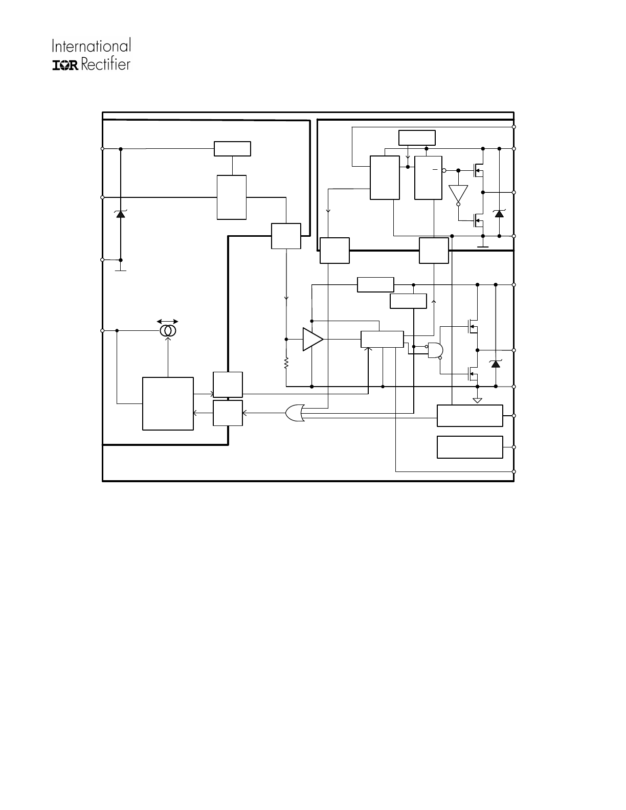
Functional Block Diagram
HIGH
SIDE
CS
VB
HO
VS
IN
LOW SIDE CS
CSD
UV
Q
UV
DETECT
DEAD-TIME
VCC
LO
COM
VDD
VSS
CSH
PROTECTION
CONTROL
SD
OCSET
UV
DETECT
UV
DETECT
CHARGE/
DISCHARGE
HV
LEVEL
SHIFT
HV
LEVEL
SHIFT
HV
LEVEL
SHIFT
FLOATING INPUT
FLOATING HIGH SIDE
HV
LEVEL
SHIFT
HV
LEVEL
SHIFT
5V REG
DT
DT
INPUT
LOGIC
10.2V
1
5
.3
V
2
0
.4
V
VREF
5.1V REFERENCE
IRS20957S
www.irf.com
© 2008 International Rectifier
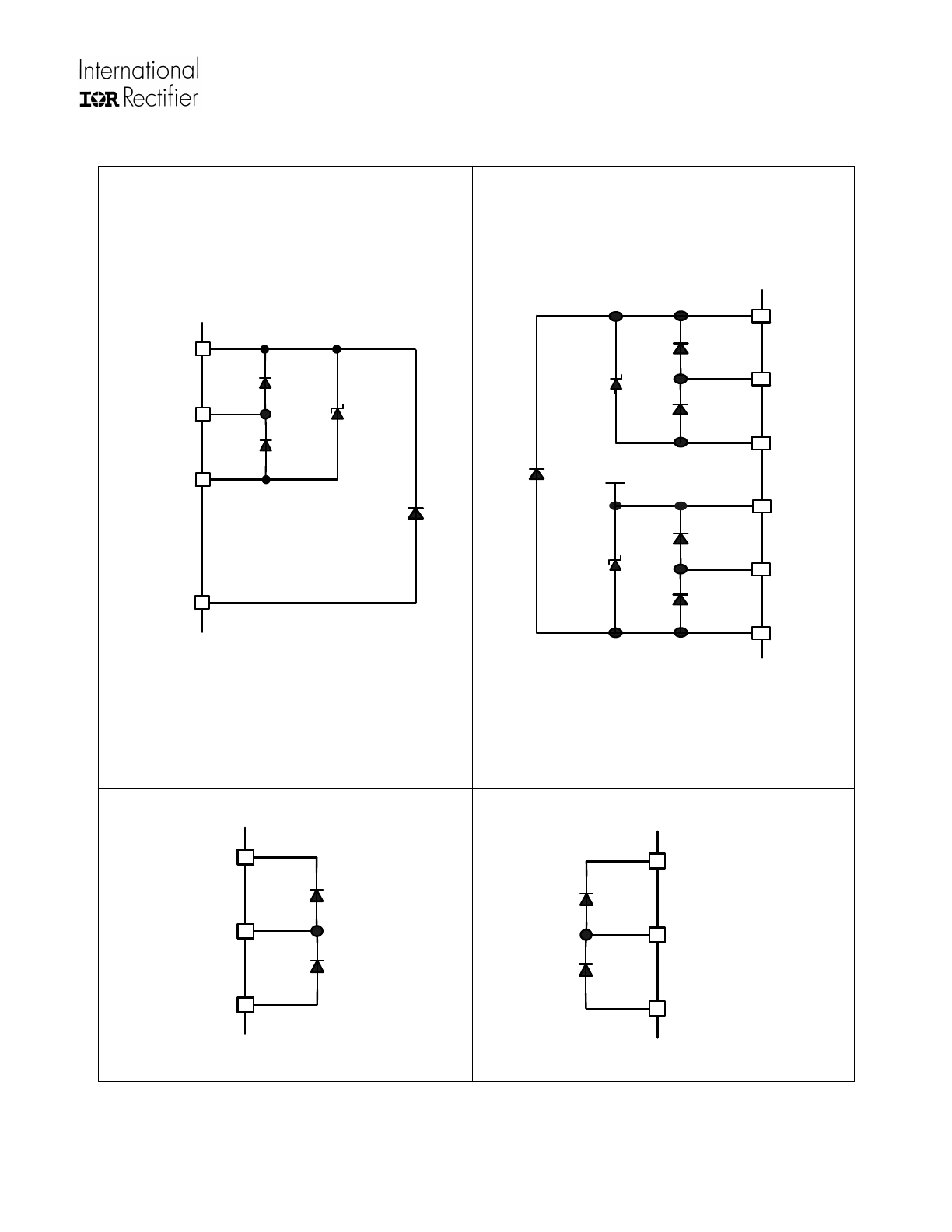
10
I/O Pin Equivalent Circuit Diagrams
ESD
Diode
ESD
Diode
VDD
CSD
VSS
10V
Clamp
VSS
215 V
ESD
Diode
ESD
Diode
VB
HO
VS
ESD
Diode
ESD
Diode
LO
COM
215 V
15 V
Clamp
20 V
Clamp
V
CC
VCC
ESD
Diode
ESD
Diode
VCC
DT, VREF
or
OCSET
COM
ESD
Diode
ESD
Diode
VB
CSH
VS