

Datasheet
Rev. 1.0, 2011-11-16
ILD4071
700mA High Integration - DC/DC Step-Down Converter
LED Driver for High Power LEDs

Datasheet
2
Rev. 1.0, 2011-11-16
ILD4071
Table of Contents
1
Overview . . . . . . . . . . . . . . . . . . . . . . . . . . . . . . . . . . . . . . . . . . . . . . . . . . . . . . . . . . . . . . . . . . . . . . . 3
2
Block Diagram . . . . . . . . . . . . . . . . . . . . . . . . . . . . . . . . . . . . . . . . . . . . . . . . . . . . . . . . . . . . . . . . . . . 5
3
Pin Configuration . . . . . . . . . . . . . . . . . . . . . . . . . . . . . . . . . . . . . . . . . . . . . . . . . . . . . . . . . . . . . . . . 6
3.1
Pin Assignment . . . . . . . . . . . . . . . . . . . . . . . . . . . . . . . . . . . . . . . . . . . . . . . . . . . . . . . . . . . . . . . . . . . 6
3.2
Pin Definitions and Functions . . . . . . . . . . . . . . . . . . . . . . . . . . . . . . . . . . . . . . . . . . . . . . . . . . . . . . . . 6
4
General Product Characteristics . . . . . . . . . . . . . . . . . . . . . . . . . . . . . . . . . . . . . . . . . . . . . . . . . . . . 8
4.1
Absolute Maximum Ratings . . . . . . . . . . . . . . . . . . . . . . . . . . . . . . . . . . . . . . . . . . . . . . . . . . . . . . . . . 8
4.2
Functional Range . . . . . . . . . . . . . . . . . . . . . . . . . . . . . . . . . . . . . . . . . . . . . . . . . . . . . . . . . . . . . . . . . 9
4.3
Thermal Resistance . . . . . . . . . . . . . . . . . . . . . . . . . . . . . . . . . . . . . . . . . . . . . . . . . . . . . . . . . . . . . . . 9
5
Electrical Characteristics . . . . . . . . . . . . . . . . . . . . . . . . . . . . . . . . . . . . . . . . . . . . . . . . . . . . . . . . . 10
5.1
General Parameters . . . . . . . . . . . . . . . . . . . . . . . . . . . . . . . . . . . . . . . . . . . . . . . . . . . . . . . . . . . . . . 10
5.2
Power Supply Monitoring . . . . . . . . . . . . . . . . . . . . . . . . . . . . . . . . . . . . . . . . . . . . . . . . . . . . . . . . . . 11
6
Enable, Dimming Function and Thermal Protection . . . . . . . . . . . . . . . . . . . . . . . . . . . . . . . . . . . 12
6.1
Description . . . . . . . . . . . . . . . . . . . . . . . . . . . . . . . . . . . . . . . . . . . . . . . . . . . . . . . . . . . . . . . . . . . . . 12
6.2
Electrical Characteristics Enable, Bias, Dimming Function and Thermal Protection . . . . . . . . . . . . . 13
6.2.1
PWM Dimming with µC connected to ILD4071 PWMI pin . . . . . . . . . . . . . . . . . . . . . . . . . . . . . . . . 14
6.2.2
Internal PWM dimming Function . . . . . . . . . . . . . . . . . . . . . . . . . . . . . . . . . . . . . . . . . . . . . . . . . . . 15
6.3
Overtemperature Protection of the Device . . . . . . . . . . . . . . . . . . . . . . . . . . . . . . . . . . . . . . . . . . . . . 16
7
Open Load Diagnosis . . . . . . . . . . . . . . . . . . . . . . . . . . . . . . . . . . . . . . . . . . . . . . . . . . . . . . . . . . . . 17
7.1
Description . . . . . . . . . . . . . . . . . . . . . . . . . . . . . . . . . . . . . . . . . . . . . . . . . . . . . . . . . . . . . . . . . . . . . 17
7.2
Electrical Characteristics: Open Load Diagnosis . . . . . . . . . . . . . . . . . . . . . . . . . . . . . . . . . . . . . . . . 17
7.3
Open Load Diagnosis . . . . . . . . . . . . . . . . . . . . . . . . . . . . . . . . . . . . . . . . . . . . . . . . . . . . . . . . . . . . . 18
8
Application Information . . . . . . . . . . . . . . . . . . . . . . . . . . . . . . . . . . . . . . . . . . . . . . . . . . . . . . . . . . 19
8.1
Output Peak Current Adjustment via R
SET
. . . . . . . . . . . . . . . . . . . . . . . . . . . . . . . . . . . . . . . . . . . . . 19
8.2
Switching Frequency Determination . . . . . . . . . . . . . . . . . . . . . . . . . . . . . . . . . . . . . . . . . . . . . . . . . . 20
8.3
ILD4071 in LED Application . . . . . . . . . . . . . . . . . . . . . . . . . . . . . . . . . . . . . . . . . . . . . . . . . . . . . . . . 22
9
Package Outlines . . . . . . . . . . . . . . . . . . . . . . . . . . . . . . . . . . . . . . . . . . . . . . . . . . . . . . . . . . . . . . . 23
10
Revision History . . . . . . . . . . . . . . . . . . . . . . . . . . . . . . . . . . . . . . . . . . . . . . . . . . . . . . . . . . . . . . . . 24
Table of Contents
PG-DSO-8 EP
Type
Package
Marking
ILD4071
PG-DSO-8 EP
ILD4071
Datasheet
3
Rev. 1.0, 2011-11-16
700mA High Integration - DC/DC Step-Down Converter
ILD4071
1
Overview
•
Constant Current Generation
•
Wide Input Voltage Range from 5V to 40V
•
Peak Current Regulation
•
Very low current consumption (<2uA) in Sleep Mode
•
Integrated power transistor with low saturation voltage
•
Integrated fast freewheeling diode
•
Integrated load current sense resistor
•
Integrated status pull down transistor
•
Overtemperature Protection
•
Switching frequency (typ. 200kHz) adjustable via external RC network
•
External PWM Dimming Input
•
Integrated PWM Dimming Engine
•
Analog Dimming (output current adjustable via external low power resistor and possibility to connect PTC
resistor for LED protection during overtemperature conditions)
•
Stable switching frequency due to fix OFF-time concept with V
REC
(supply voltage) feedforward
•
Under- and Overvoltage shutdown with hysteresis
•
Small thermally enhanced exposed heatslug SMD package
•
Green Product (RoHS) Compliant
Description
The ILD4071 is a highly integrated smart LED buck controller with built in protection functions. The main function
of this device is to drive single or multiple series connected LEDs efficiently from a voltage source higher than the
LED forward voltage by regulating a constant LED current. The constant current regulation is especially beneficial
for LED color accuracy and long LED lifetime. The built in freewheeling diode and switching transistor with current
sense requires less external components and saves system costs. High flexibility is achieved by placing low power
resistors to adjust output currents up to 700mA and the regulator switching frequency (typ. 200kHz). An integrated
PWM dimming engine provides a LED dimming function by placing a simple RC network to GND. This feature is
dedicated for simple decentralized light modules without micro controller involvement.

Datasheet
4
Rev. 1.0, 2011-11-16
ILD4071
Overview
Applications
•
LED Controller for Industrial Applications
•
Universal Constant Current and Voltage Source
•
General Illumination e.g. Halogen Replacement
•
Residential Architectural and Industrial Commercial Lighting for in- and outdoor
•
Signal and Marker Lights for Orientation or Navigation (e.g. steps, exit ways, etc.)
For automotive and transportation applications, please refer to the Infineon® Auto LED products.
ILD4071
Block Diagram
Datasheet
5
Rev. 1.0, 2011-11-16
2
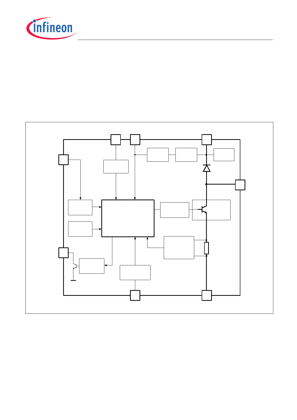
Block Diagram
The ILD4071 regulates the LED current by monitoring the load current (Peak Current Measurement) through the
internal switch cycle by cycle. When the current through the switch reaches the threshold I
peak
the switch is shut-
OFF and it is kept OFF for a time equal to t
OFF
. Both I
peak
and t
OFF
can be fixed through few external components.
The peak current I
peak
is fixed by a resistor connected to the SET pin while the t
OFF
is fixed by RC network. As t
OFF
is fixed and the duty cycle depends on V
REC
, the frequency depends on V
REC
as well. Refer to
Chapter 8.2
for the
evaluation of the switching frequency.
Figure 1
Block Diagram ILD4071
1
5
3
2
8
7
6
GND
VREC
Logic
Power
Switch
FREQ
SW
Internal
Supply
EN
Thermal
Protection
UV+OV
Lockout
SET
PWMI
ST
Power-
Switch Driver
Open Load
Detection
Peak Current
Measurement
ON/OFF
Logic
Peak Current
Adjustment
4
OFF-Time
Control
internal
PWM
Generation
Datasheet
6
Rev. 1.0, 2011-11-16
ILD4071
Pin Configuration
3
Pin Configuration
3.1
Pin Assignment
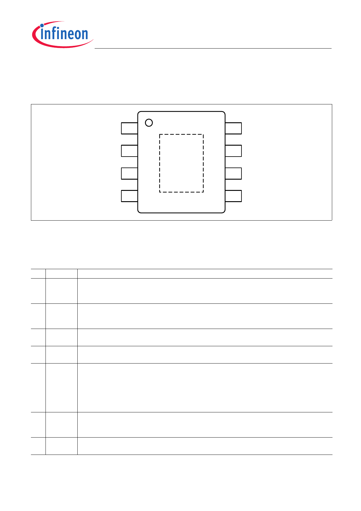
Figure 2
Pin Configuration ILD4071
3.2
Pin Definitions and Functions
Pin
Symbol
Function
1
VREC
Voltage Recirculation Output and Internal Supply Input;
This pin is the supply pin of the IC (see block diagram). Furthermore the cathode of the
integrated fast freewheeling diode is connected to this pin as well.
2
ST
Status Output;
Open collector diagnostic output to indicate an open load failure.
Refer to
Chapter 7
for more details.
3
EN
Enable;
Apply logic HIGH signal to enable the device
4
SET
SET Input;
Connect a low power resistor to adjust the output current.
5
PWMI
PWM Input;
PWM signal for dimming LEDs. Connect external R and C combination to achieve an auto
PWM-dimming function with defined frequency and duty cycle.
1) internal PWM dimming function (external RC connected to GND)
2) external PWM dimming function (µC is controlling this pin)
Refer to
Chapter 6
for more details.
6
FREQ
FREQuency Select Input;
Connect external Resistor and Capacitor to GND to set the OFF-time of the switching
frequency.
7
GND
Ground;
Connect to system ground.
ST
GND
EN
FREQ
SW
5
6
4
3
2
7
1
8
SET
VREC
PWMI
EP

ILD4071
Pin Configuration
Datasheet
7
Rev. 1.0, 2011-11-16
8
SW
Integrated Power-Switch Output;
Collector of the integrated NPN-power transistor.
EP
Exposed Pad;
Connect to external heatspreading copper area with electrically GND (e.g. inner GND layer of
the PCB via thermal vias)
Pin
Symbol
Function
Datasheet
8
Rev. 1.0, 2011-11-16
ILD4071
General Product Characteristics
4
General Product Characteristics
4.1
Absolute Maximum Ratings
Note: Stresses above the ones listed here may cause permanent damage to the device. Exposure to absolute
maximum rating conditions for extended periods may affect device reliability.
Note: Integrated protection functions are designed to prevent IC destruction under fault conditions described in the
data sheet. Fault conditions are considered as “outside” normal operating range. Protection functions are
not designed for continuous repetitive operation.
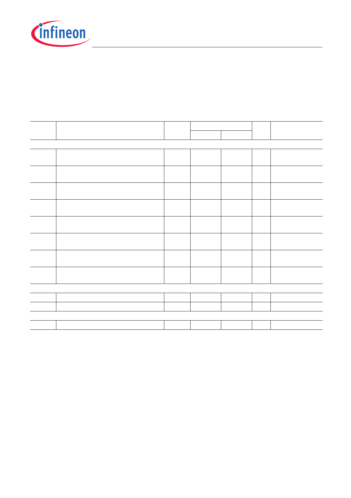
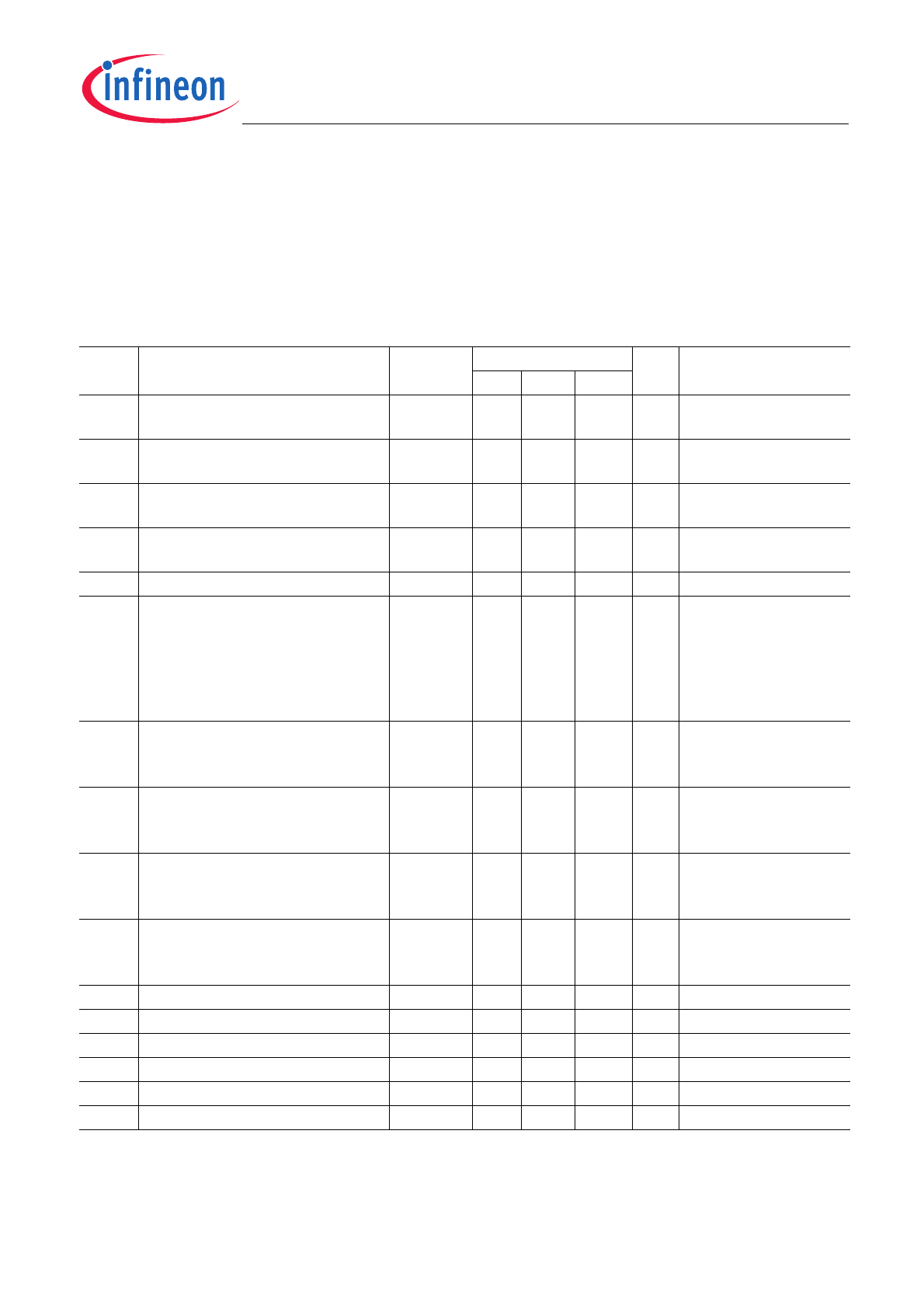
Absolute Maximum Ratings
1)
T
j
= -40
°C to +125 °C; all voltages with respect to ground (unless otherwise specified)
1) Not subject to production test, specified by design.
Pos.
Parameter
Symbol
Limit Values
Unit
Conditions
Min.
Max.
Voltages
4.1.1
VREC (Pin 1)
Recirculation and Supply Input
V
REC
-0.3
45
V
–
4.1.2
ST (Pin 2)
Diagnostic Status Output Voltage
V
ST
-0.3
45
V
–
4.1.3
ST (Pin 2)
Diagnostic Status Current
I
ST
–
150
mA
–
4.1.4
EN (Pin 3)
Enable Input Voltage
V
EN
-0.3
45
V
–
4.1.5
SET (Pin 4)
Peak Current Adjust Input Voltage
V
SET
-0.3
6
V
–
4.1.6
PWMI (Pin 5)
PWM Input Voltage
V
PWMI
-0.3
6
V
–
4.1.7
FREQ (Pin 6)
OFF-time Adjustment Input
V
FREQ
-0.3
6
V
–
4.1.8
SW (Pin 8)
Switch Output
V
SW
-0.3
45
V
–
Temperatures
4.1.9
Junction Temperature
T
j
-40
150
°C
–
4.1.10
Storage Temperature
T
stg
-55
150
°C
–
ESD Susceptibility
4.1.11
ESD Resistivity all Pins to GND
V
ESD,HBM
-2
2
kV
HBM
2)
2) ESD susceptibility HBM according to EIA/JESD 22-A 114B
ILD4071
General Product Characteristics
Datasheet
9
Rev. 1.0, 2011-11-16
4.2
Functional Range
Note: Within the functional range the IC operates as described in the circuit description. The electrical
characteristics are specified within the conditions given in the related electrical characteristics table.
4.3
Thermal Resistance
Note: This thermal data was generated in accordance with JEDEC JESD51 standards.
For more information, go to
www.jedec.org
.
Pos.
Parameter
Symbol
Limit Values
Unit
Conditions
Min.
Max.
4.2.1
Supply Voltage Range
V
REC
5
40
1)
1) Not subject to production test, specified by design.
–
4.2.2
Output current range
I
OUT
100
700
mA
–
4.2.3
Switching Frequency
f
SW
50
300
1)
kHz
T
j
= 25°C to 150°C
4.2.4
Junction Temperature
T
j
-40
125
°C
–
Pos.
Parameter
Symbol
Limit Values
Unit
Conditions
Min.
Typ.
Max.
4.3.1
Junction to Case
R
thJ-case
–
10
–
K/W
1)
2)
1) Not subject to production test, specified by design.
2) Specified
R
thJ-case
value is simulated at natural convection on a cold plate setup (all pins and the exposed Pad are fixed to
ambient temperature). Ta=25°C, Power Switch and freewheeling diode are dissipating 1W.
4.3.2
Junction to Ambient (2s2p)
R
thJA
–
40
–
K/W
1)
3)
3) Specified RthJA value is according to Jedec JESD51-2,-7 at natural convection on FR4 2s2p board; The Product
(Chip+Package) was simulated on a 76.2 x 114.3 x 1.5 mm board with 2 inner copper layers (2 x 70µm Cu, 2 x 35µm Cu).
According to JESD51-5 a thermal via array under the exposed pad contacted the first inner copper layer. Ta=25°C, Power
Switch and freewheeling diode are dissipating 1W.
Datasheet
10
Rev. 1.0, 2011-11-16
ILD4071
Electrical Characteristics
5
Electrical Characteristics
All parameters have been tested at 25°C, unless otherwise specified.
5.1
General Parameters
Electrical Characteristics: Buck Regulator
V
REC
= 24 V,
T
j
= -40
°C to +125 °C, all voltages with respect to ground (unless otherwise specified)
Pos.
Parameter
Symbol
Limit Values
Unit Conditions
Min.
Typ.
Max.
5.1.1
Voltage Drop over Power
Transistor
V
Drop,100
–
0.8
–
V
I
peak
=100mA
5.1.2
Voltage Drop over Power
Transistor
V
Drop,700
–
1.4
–
V
I
peak
=700mA
5.1.3
Freewheeling diode forward
voltage
V
fw,100
–
0.8
–
V
I
peak
=100mA
5.1.4
Freewheeling diode forward
voltage
V
fw,700
–
1.4
–
V
I
peak
=700mA
5.1.5
Peak over current limit
I
peak_lim
–
1.4
–
A
–
5.1.6
Peak current accuracy
I
peak_acc
450
500
550
mA
V
REC
= 12V
V
EN
= 5V
V
LED
= 7.2V
R
SET
= 14k
Ω
L
SW
= 220µH
f
SW
= 200kHz
5.1.7
Input under voltage shutdown
threshold
V
REC,UVOFF
–
–
5
V
V
EN
= 5V
V
REC
decreasing; see
Figure 3
5.1.8
Input voltage startup threshold
V
REC,UVON
–
–
6
V
V
EN
= 5V
V
REC
increasing; see
Figure 3
5.1.9
Input over voltage shutdown
threshold
V
REC,OVOFF
40.5
–
–
V
V
EN
= 5V
V
REC
increasing; see
Figure 3
5.1.10
Input over voltage startup threshold
V
REC,OV
40
–
–
V
V
EN
= 5V
V
REC
decreasing; see
Figure 3
5.1.11
Switch ON delay
t
dON
–
400
600
ns
1)
–
1) The minimum switching ON time t
ON
must be greater than t
dON
+ t
dOFF
5.1.12
Switch OFF delay
t
dOFF
–
500
850
ns
1)
–
5.1.13
Reference Voltage at SET pin
V
SET
1.16
1.225 1.29
V
–
5.1.14
Pull up current for FREQ pin
I
FREQ
5
–
–
mA
V
FREQ
=0V
5.1.15
Oscillator switch off threshold
V
FREQ,HIGH
–
3.2
–
V
–
5.1.16
Oscillator switch on threshold
V
FREQ,LOW
–
1.2
–
V
–