

Standard Power
Data Sheet
Rev. 1.0, 2011-04-08
IFX1050GVIO
High Speed CAN-Transceiver

Data Sheet
2
Rev. 1.0, 2011-04-08
IFX1050GVIO
Table of Contents
1
Overview . . . . . . . . . . . . . . . . . . . . . . . . . . . . . . . . . . . . . . . . . . . . . . . . . . . . . . . . . . . . . . . . . . . . . . . 3
2
Pin Configuration . . . . . . . . . . . . . . . . . . . . . . . . . . . . . . . . . . . . . . . . . . . . . . . . . . . . . . . . . . . . . . . . 4
3
Block Diagram . . . . . . . . . . . . . . . . . . . . . . . . . . . . . . . . . . . . . . . . . . . . . . . . . . . . . . . . . . . . . . . . . . . 5
4
Electrical Characteristics . . . . . . . . . . . . . . . . . . . . . . . . . . . . . . . . . . . . . . . . . . . . . . . . . . . . . . . . . . 6
4.1
Operating Range . . . . . . . . . . . . . . . . . . . . . . . . . . . . . . . . . . . . . . . . . . . . . . . . . . . . . . . . . . . . . . . . . 6
5
Diagrams . . . . . . . . . . . . . . . . . . . . . . . . . . . . . . . . . . . . . . . . . . . . . . . . . . . . . . . . . . . . . . . . . . . . . . 11
6
Application Information . . . . . . . . . . . . . . . . . . . . . . . . . . . . . . . . . . . . . . . . . . . . . . . . . . . . . . . . . . 13
7
Package Outlines . . . . . . . . . . . . . . . . . . . . . . . . . . . . . . . . . . . . . . . . . . . . . . . . . . . . . . . . . . . . . . . 17
8
Revision History . . . . . . . . . . . . . . . . . . . . . . . . . . . . . . . . . . . . . . . . . . . . . . . . . . . . . . . . . . . . . . . . 18
Table of Contents
PG-DSO-8
Type
Package
Marking
IFX1050GVIO
PG-DSO-8
1050IO
Data Sheet
3
Rev. 1.0, 2011-04-08
High Speed CAN-Transceiver
IFX1050GVIO
1
Overview
Features
•
CAN data transmission rate up to 1 MBaud
•
Stand-by Mode
•
Suitable for 12 V and 24 V applications
•
Excellent EMC performance (very high immunity and very low
emission)
•
Bus pins are short circuit proof to ground and battery voltage
•
Versions for 5V and 3.3V microcontrollers
•
Overtemperature protection
•
Green Product (RoHS compliant)
Description
The HS CAN-transceiver IFX1050GVIO is optimized for high speed differential mode data transmission in
industrial applications and is compatible to ISO/DIS 11898. It works as an interface between the CAN protocol
controller and the physical differential bus in both, 12 V and 24 V systems.
The IFX1050GVIO is designed to withstand the conditions of industrial applications and provides excellent EMC
performance.
IFX1050GVIO
3.3 V logic I/O version (logic I/O voltage adaptive to
V
33
pin within the range 3.3 V to 5 V):
RxD, TxD, INH. One control pin (INH) and two operation modes: Normal Mode and Standby Mode.
Data Sheet
4
Rev. 1.0, 2011-04-08
IFX1050GVIO
Pin Configuration
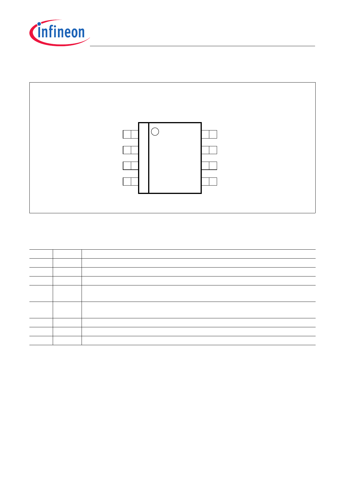
2
Pin Configuration
Figure 1
Pin Configuration IFX1050GVIO (top view)
Table 1
Pin Definitions and Functions IFX1050GVIO
Pin No. Symbol
Function
1
TxD
CAN transmit data input; 20 k
Ω pull-up, LOW in dominant state
2
GND
Ground
3
V
CC
5 V Supply input
4
RxD
CAN receive data output; LOW in dominant state,
integrated pull-up
5
V
33V
Logic supply input; 3.3V or 5V microcontroller logic supply can be connected here! The
digital I/Os of the IFX1050GVIO adopt to the connected microcontroller logic supply a
V
33V
6
CANL
Low line I/O; LOW in dominant state
7
CANH
High line I/O; HIGH in dominant state
8
INH
Inhibit Input; control input, 20 k
Ω pull, set LOW for normal mode
1
TxD
2
GND
3
V
CC
4
RxD
8
7
6
5
CANH
CANL
INH
V
33V
IFX1050GVIO
(PG-DSO-8)
IFX1050GVIO
Block Diagram
Data Sheet
5
Rev. 1.0, 2011-04-08
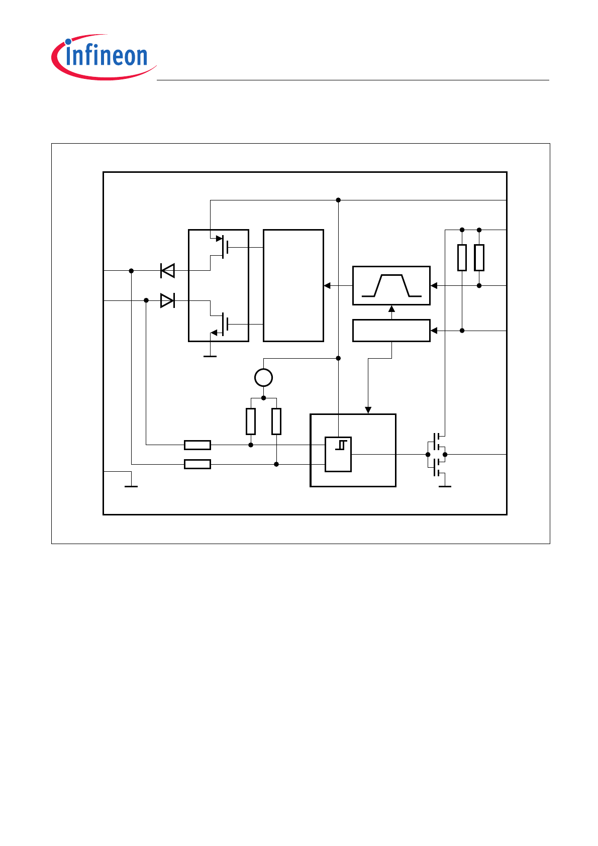
3
Block Diagram
Figure 2
Block Diagram IFX1050GVIO
IFX1050GVIO
Receiver
Output
Stage
Driver
Temp-
Protection
Mode Control
*
=
7
CANH
6
CANL
2
GND
TxD
1
3
V
CC
INH
8
RxD
4
5
V
33
Data Sheet
6
Rev. 1.0, 2011-04-08
IFX1050GVIO
Electrical Characteristics
4
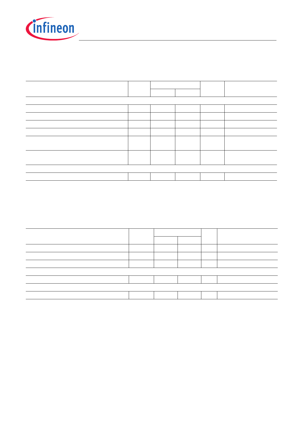
Electrical Characteristics
Note: Maximum ratings are absolute ratings; exceeding any one of these values may cause irreversible damage
to the integrated circuit.
4.1
Operating Range
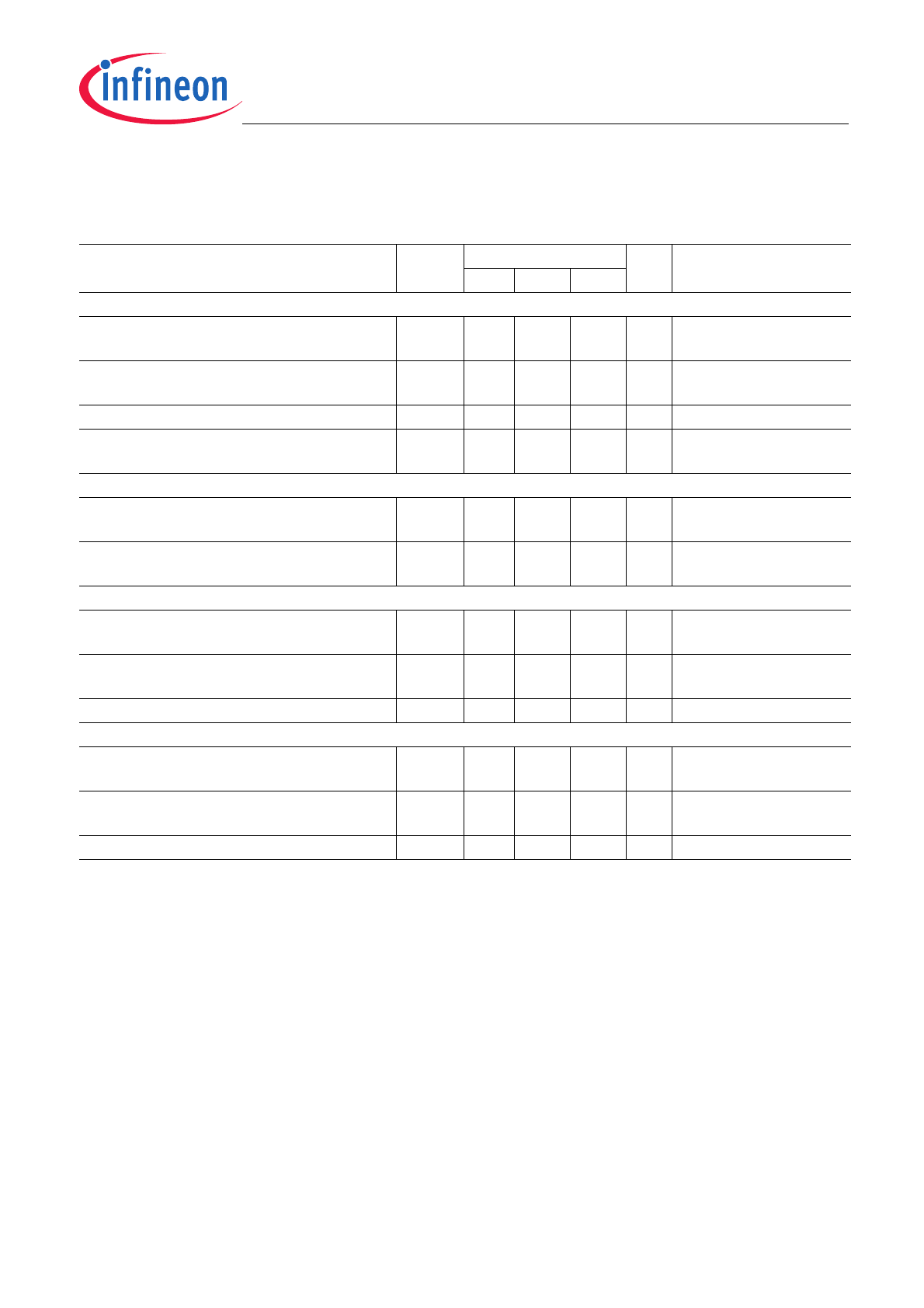
Table 2
Absolute Maximum Ratings
Parameter
Symbol
Limit Values
Unit
Remarks
Min.
Max.
Voltages
Supply voltage
V
CC
-0.3
6.5
V
–
3.3V supply
V
33V
-0.3
6.5
V
–
CAN input voltage (CANH, CANL)
V
CANH/L
-40
40
V
–
Logic voltages at INH, RM, TxD, RxD
V
I
-0.3
V
CC
V
0 V <
V
CC
< 5.5 V
Electrostatic discharge voltage at CANH,
CANL
V
ESD
-6
6
kV
human body model
(100 pF via 1.5 k
Ω)
Electrostatic discharge voltage
V
ESD
-2
2
kV
human body model
(100 pF via 1.5 k
Ω)
Temperatures
Junction temperature
T
j
-40
150
°C
–
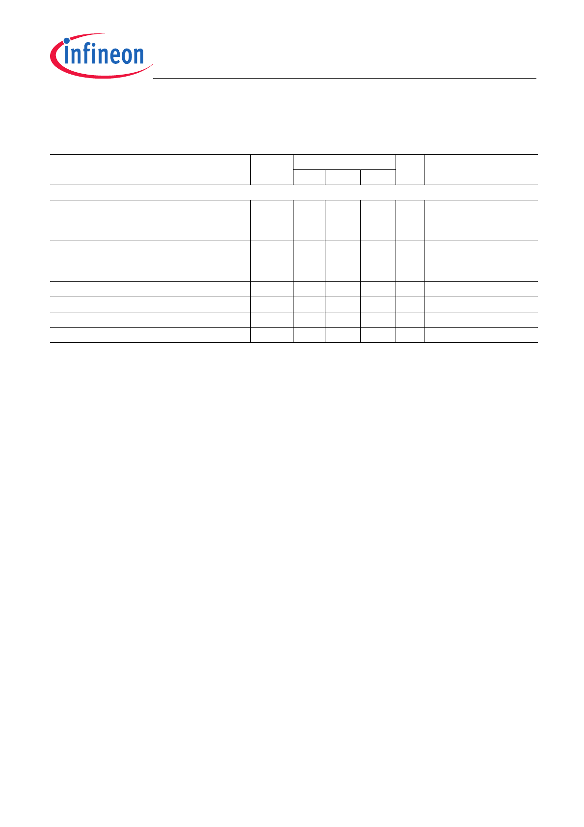
Table 3
Operating Range
Parameter
Symbol
Limit Values
Unit
Remarks
Min.
Max.
Supply voltage
V
CC
4.5
5.5
V
–
3.3V supply voltage
V
33V
3.0
5.5
V
–
Junction temperature
T
j
-40
125
°C
–
Thermal Resistances
Junction ambient
R
thj-a
–
185
K/W
–
Thermal Shutdown (junction temperature)
Thermal shutdown temperature
T
jsD
160
200
°C
10
°C hysteresis
IFX1050GVIO
Electrical Characteristics
Data Sheet
7
Rev. 1.0, 2011-04-08
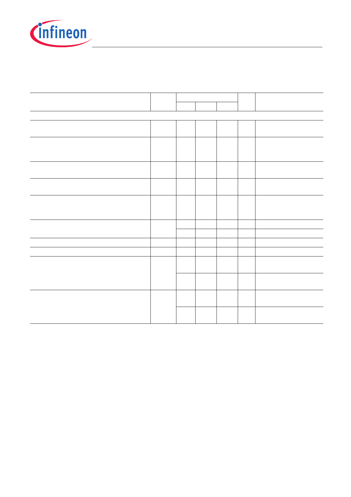
Table 4
Electrical Characteristics
4.5 V <
V
CC
< 5.5 V; 3.0 V <
V
33V
< 5.5 V
R
L
= 60
Ω;
V
INH
<
V
INH,ON
; -40
°C <
T
j
< 125
°C; all voltages with respect
to ground; positive current flowing into pin; unless otherwise specified.
Parameter
Symbol
Limit Values
Unit Remarks
Min.
Typ.
Max.
Current Consumption
Current consumption
I
CC+33V
–
6
10
mA
recessive state;
V
TxD
=
V
33V
Current consumption
I
CC+33V
–
45
70
mA
dominant state;
V
TxD
= 0 V
Current consumption
I
33V
–
–
2
mA
–
Current consumption
I
CC+33V,stb
–
1
10
μA
stand-by mode;
TxD = high
Receiver Output RxD
HIGH level output current
I
RD,H
–
-2
-1
mA
V
RD
= 0.8
×
V
33V
,
V
diff
< 0.4 V
1)
LOW level output current
I
RD,L
1
2
–
mA
V
RD
= 0.2
×
V
33V
,
V
diff
> 1 V
1)
Transmission Input TxD
HIGH level input voltage threshold
V
TD,H
–
0.55
×
V
33V
0.7
×
V
33V
V
recessive state
LOW level input voltage threshold
V
TD,L
0.3
×
V
33V
0.45
×
V
33V
–
V
dominant state
TxD pull-up resistance
R
TD
10
25
50
k
Ω
–
Inhibit Input (pin INH)
HIGH level input voltage threshold
V
INH,H
–
0.55
×
V
33V
0.7
×
V
33V
V
stand-by mode;
LOW level input voltage threshold
V
INH,L
0.3
×
V
33V
0.45
×
V
33V
–
V
normal mode
INH pull-up resistance
R
INH
10
25
50
k
Ω
–
Data Sheet
8
Rev. 1.0, 2011-04-08
IFX1050GVIO
Electrical Characteristics
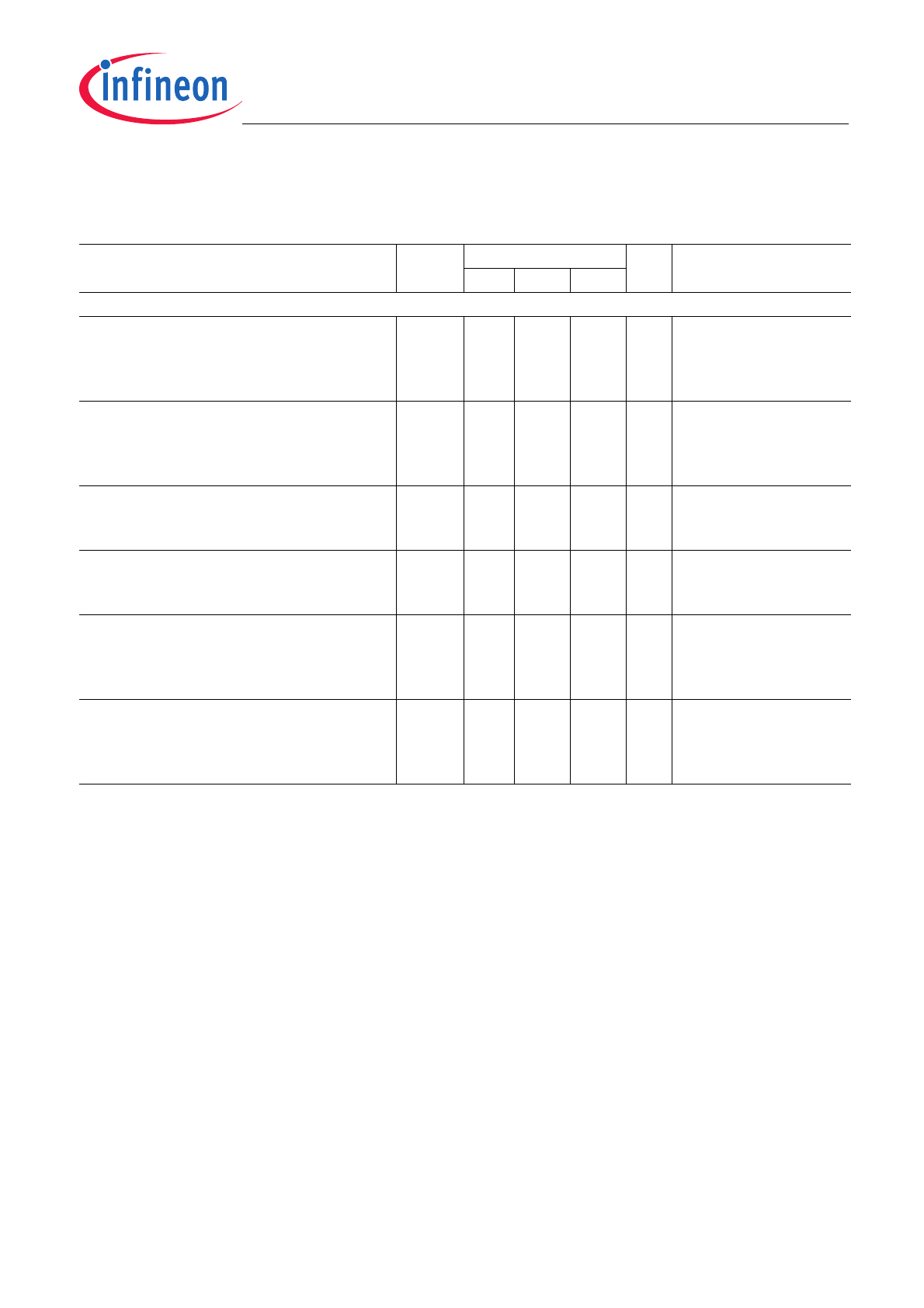
Bus Receiver
Differential receiver threshold voltage,
recessive to dominant edge
V
diff,d
–
0.75
0.90
V
-20 V < (
V
CANH
,
V
CANL
) <
25 V
V
diff
=
V
CANH
-
V
CANL
Differential receiver threshold voltage
dominant to recessive edge
V
diff,r
0.50
0.60
–
V
-20 V < (
V
CANH
,
V
CANL
) <
25 V
V
diff
=
V
CANH
-
V
CANL
Common Mode Range
CMR
-20
–
25
V
V
CC
= 5 V
Differential receiver hysteresis
V
diff,hys
–
150
–
mV
–
CANH, CANL input resistance
R
i
10
20
30
k
Ω
recessive state
Differential input resistance
R
diff
20
40
60
k
Ω
recessive state
Table 4
Electrical Characteristics (cont’d)
4.5 V <
V
CC
< 5.5 V; 3.0 V <
V
33V
< 5.5 V
R
L
= 60
Ω;
V
INH
<
V
INH,ON
; -40
°C <
T
j
< 125
°C; all voltages with respect
to ground; positive current flowing into pin; unless otherwise specified.
Parameter
Symbol
Limit Values
Unit Remarks
Min.
Typ.
Max.
IFX1050GVIO
Electrical Characteristics
Data Sheet
9
Rev. 1.0, 2011-04-08
Bus Transmitter
CANL/CANH recessive output voltage
V
CANL/H
0.4
×
V
CC
–
0.6
×
V
CC
V
V
TxD
=
V
33V
CANH, CANL recessive output voltage
difference
V
diff
=
V
CANH
-
V
CANL
, no load
2)
V
diff
-1
–
0.05
V
V
TxD
=
V
33V
CANL dominant output voltage
V
CANL
–
–
2.0
V
V
TxD
= 0 V;
V
CC
= 5 V
CANH dominant output voltage
V
CANH
2.8
–
–
V
V
TxD
= 0 V;
V
CC
= 5 V
CANH, CANL dominant output voltage
difference
V
diff
=
V
CANH
-
V
CANL
V
diff
1.5
–
3.0
V
V
TxD
= 0 V;
V
CC
= 5 V
CANL short circuit current
I
CANLsc
50
120
200
mA
V
CANLshort
= 18 V
–
150
–
mA
V
CANLshort
= 36 V
CANH short circuit current
I
CANHsc
-200
-120
-50
mA
V
CANHshort
= 0 V
CANH short circuit current
I
CANHsc
–
-120
–
mA
V
CANHshort
= -5 V
Output current
I
CANH/L,lk
-50
-300
-400
μA
V
CC
= 0 V,
V
CANH
=
V
CANL
= -7 V
-50
-100
-150
μA
V
CC
= 0 V,
V
CANH
=
V
CANL
= -2 V
Output current
I
CANH/L,lk
50
280
400
μA
V
CC
= 0 V,
V
CANH
=
V
CANL
= 7 V
50
100
150
μA
V
CC
= 0 V,
V
CANH
=
V
CANL
= 2 V
Table 4
Electrical Characteristics (cont’d)
4.5 V <
V
CC
< 5.5 V; 3.0 V <
V
33V
< 5.5 V
R
L
= 60
Ω;
V
INH
<
V
INH,ON
; -40
°C <
T
j
< 125
°C; all voltages with respect
to ground; positive current flowing into pin; unless otherwise specified.
Parameter
Symbol
Limit Values
Unit Remarks
Min.
Typ.
Max.
Data Sheet
10
Rev. 1.0, 2011-04-08
IFX1050GVIO
Electrical Characteristics
Dynamic CAN-Transceiver Characteristics
Propagation delay TxD-to-RxD LOW
(recessive to dominant)
t
d(L),TR
–
150
280
ns
C
L
= 47 pF;
R
L
= 60
Ω;
V
CC
= 5 V;
C
RxD
= 20 pF
Propagation delay TxD-to-RxD HIGH
(dominant to recessive)
t
d(H),TR
–
150
280
ns
C
L
= 47 pF;
R
L
= 60
Ω;
V
CC
= 5 V;
C
RxD
= 20 pF
Propagation delay
TxD LOW to bus dominant
t
d(L),T
–
100
140
ns
C
L
= 47 pF;
R
L
= 60
Ω;
V
CC
= 5 V
Propagation delay
TxD HIGH to bus recessive
t
d(H),T
–
100
140
ns
C
L
= 47 pF;
R
L
= 60
Ω;
V
CC
= 5 V
Propagation delay bus dominant to RxD LOW
t
d(L),R
–
50
140
ns
C
L
= 47 pF;
R
L
= 60
Ω;
V
CC
= 5 V;
C
RxD
= 20 pF
Propagation delay bus recessive to RxD
HIGH
t
d(H),R
–
50
140
ns
C
L
= 47 pF;
R
L
= 60
Ω;
V
CC
= 5 V;
C
RxD
= 20 pF
1)
V
diff
=
V
CANH
-
V
CANL
2) Deviation from ISO/DIS 11898
Table 4
Electrical Characteristics (cont’d)
4.5 V <
V
CC
< 5.5 V; 3.0 V <
V
33V
< 5.5 V
R
L
= 60
Ω;
V
INH
<
V
INH,ON
; -40
°C <
T
j
< 125
°C; all voltages with respect
to ground; positive current flowing into pin; unless otherwise specified.
Parameter
Symbol
Limit Values
Unit Remarks
Min.
Typ.
Max.