

CCM-PFC
ICE1PCS01
ICE1PCS01G
Standalone Power Factor
Correction (PFC) Controller in
Continuous Conduction Mode
(CCM)
N e v e r s t o p t h i n k i n g .
Datasheet, V1.3, 06 Feb 2007
P o w e r M a n a g e m e n t & S u p p l y

Edition 2007-02-06
Published by Infineon Technologies AG,
St.-Martin-Strasse 53,
D-81541 München
©
Infineon Technologies AG 1999.
All Rights Reserved.
Attention please!
The information herein is given to describe certain components and shall not be considered as warranted charac-
teristics.
Terms of delivery and rights to technical change reserved.
We hereby disclaim any and all warranties, including but not limited to warranties of non-infringement, regarding
circuits, descriptions and charts stated herein.
Infineon Technologies is an approved CECC manufacturer.
Information
For further information on technology, delivery terms and conditions and prices please contact your nearest Infi-
neon Technologies Office in Germany or our Infineon Technologies Representatives worldwide (see address list).
Warnings
Due to technical requirements components may contain dangerous substances. For information on the types in
question please contact your nearest Infineon Technologies Office.
Infineon Technologies Components may only be used in life-support devices or systems with the express written
approval of Infineon Technologies, if a failure of such components can reasonably be expected to cause the failure
of that life-support device or system, or to affect the safety or effectiveness of that device or system. Life support
devices or systems are intended to be implanted in the human body, or to support and/or maintain and sustain
and/or protect human life. If they fail, it is reasonable to assume that the health of the user or other persons may
be endangered.
For questions on technology, delivery and prices please contact the Infineon Technologies Offices in Germany or
the Infineon Technologies Companies and Representatives worldwide: see our webpage at http://
www.infineon.com
CoolMOST™, CoolSET™ are trademarks of Infineon Technologies AG.
CCM-PFC
Revision History:
2007-02-06
Datasheet
Previous Version: V1.2
Page
Subjects ( major changes since last revision )
Update package information
CCM-PFC
ICE1PCS01
ICE1PCS01G
Version 1.2
3
06 Feb 2007
Type
Package
ICE1PCS01
PG-DIP-8
ICE1PCS01G
PG-DSO-8
Standalone Power Factor Correction
(PFC) Controller in Continuous
Conduction Mode (CCM)
ICE1PCS01
PG-DIP-8
ICE1PCS01G
PG-DSO-8
Product Highlights
• Wide Input Range
• Output Power Controllable by External Sense Resistor
• Programmable Operating Frequency
• Output Under-Voltage Detection
• Fast Output Dynamic Response during LoadJumps
• Pb-free lead plating; RoHS compliant
Features
• Ease of Use with Few External Components
• Supports Wide Range
• Average Current Control
• External Current and Voltage Loop Compensation
for Greater User Flexibility
• Programmable Operating/Switching Frequency
(50kHz - 250kHz)
• Max Duty Cycle of 95% (typ) at 125kHz
• Trimmed Internal Reference Voltage (5V+2%)
• VCC Under-Voltage Lockout
• Cycle by Cycle Peak Current Limiting
• Over-Voltage Protection
• Open Loop Detection
• Output Under-Voltage Detection
• Brown-Out Protection
• Enhanced Dynamic Response
• Unique Soft-Start to Limit Start Up Current
• Fulfills Class D Requirements of IEC 1000-3-2
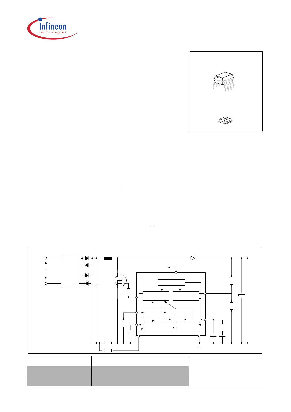
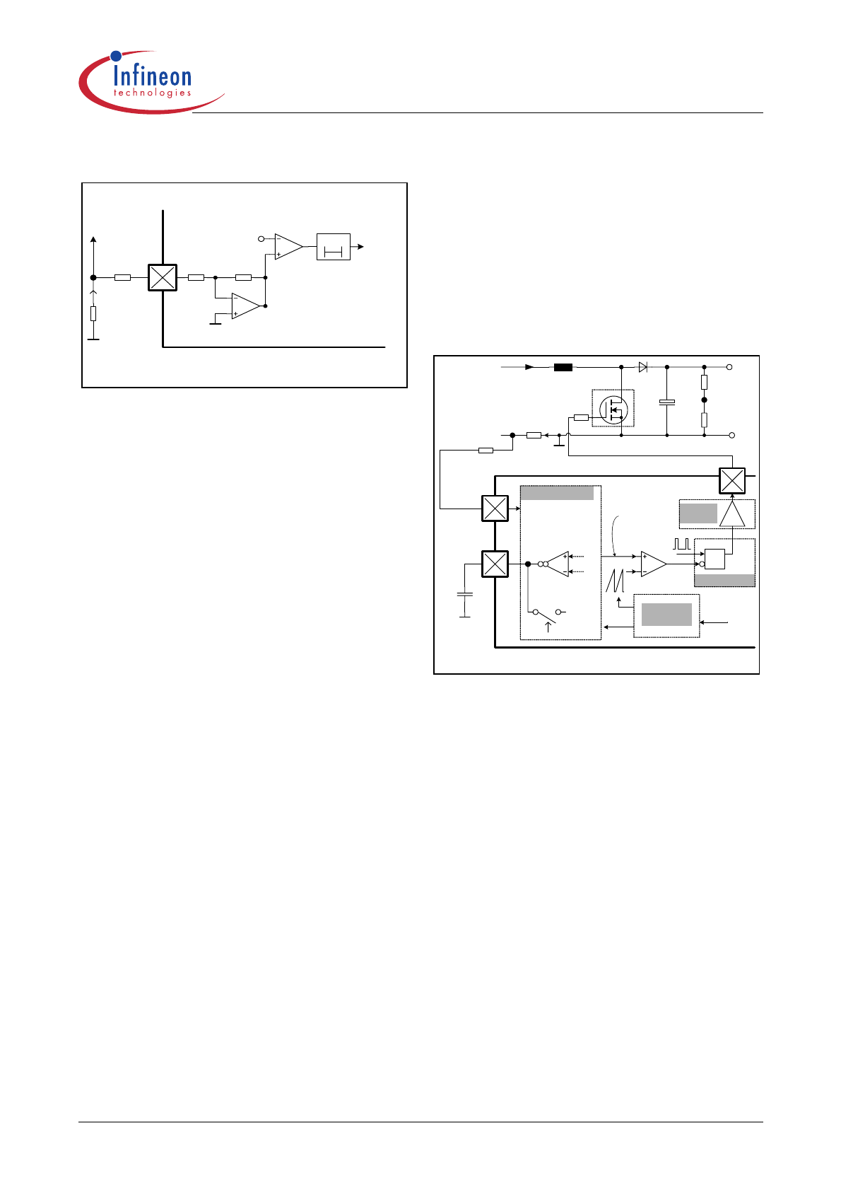
Description
The ICE1PCS01/G is a 8-pin wide input range controller
IC for active power factor correction converters. It is de-
signed for converters in boost topology, and requires few
external components. Its power supply is recommended
to be provided by an external auxiliary supply which will
switch on and off the IC.
The IC operates in the CCM with average current control,
and in DCM only under light load condition. The switching
frequency is programmable by the resistor at pin 4. Both
compensations for the current and voltage loop are exter-
nal to allow full user control.
There are various protection features incorporated to en-
sure safe system operation conditions. Examples are
peak current limitation, brown-out protection and output
under voltage detection. The internal reference is trimmed
(5V+2%) to ensure precise protection and control level.
The device has an unique soft-start function which limits
the start up current thus reducing the stress on the boost
diode.
85 ... 265 VAC
EMI-Filter
Voltage Loop
Compensation
Protection Unit
Variable
Oscillator
Current Loop
Compensation
PWM Logic
Driver
ICE1PCS01/
ICE1PCS01G
PFC-Controller
VCC
Auxiliary Supply
V
OUT
Typical Application
SWITCH
Ramp
Generator
FREQ
ICOMP
VSENSE
VCOMP
ISENSE
GND
Nonlinear
Gain
GATE

CCM-PFC
ICE1PCS01/G
Version 1.2
4
06 Feb 2007
1
Pin Configuration and Functionality . . . . . . . . . . . . . . . . . . . . . . . . . . . . .5
1.1
Pin Configuration . . . . . . . . . . . . . . . . . . . . . . . . . . . . . . . . . . . . . . . . . . . . . .5
1.2
Pin Functionality . . . . . . . . . . . . . . . . . . . . . . . . . . . . . . . . . . . . . . . . . . . . . .5
2
Representative Block diagram . . . . . . . . . . . . . . . . . . . . . . . . . . . . . . . . . .6
3
Functional Description . . . . . . . . . . . . . . . . . . . . . . . . . . . . . . . . . . . . . . . .7
3.1
General . . . . . . . . . . . . . . . . . . . . . . . . . . . . . . . . . . . . . . . . . . . . . . . . . . . . .7
3.2
Power Supply . . . . . . . . . . . . . . . . . . . . . . . . . . . . . . . . . . . . . . . . . . . . . . . . .7
3.3
Start-up (Soft-Start) . . . . . . . . . . . . . . . . . . . . . . . . . . . . . . . . . . . . . . . . . . . .7
3.4
System Protection . . . . . . . . . . . . . . . . . . . . . . . . . . . . . . . . . . . . . . . . . . . . .8
3.4.1
Brown-Out Protection (BOP) . . . . . . . . . . . . . . . . . . . . . . . . . . . . . . . . . . .8
3.4.2
Soft Over Current Control (SOC) . . . . . . . . . . . . . . . . . . . . . . . . . . . . . . . .8
3.4.3
Peak Current Limit (PCL) . . . . . . . . . . . . . . . . . . . . . . . . . . . . . . . . . . . . . .8
3.4.4
Open Loop Protection / Input Under Voltage Protect (OLP) . . . . . . . . . . .9
3.4.5
Output Under Voltage Detection (OUV) . . . . . . . . . . . . . . . . . . . . . . . . . . .9
3.4.6
Over-Voltage Protection (OVP) . . . . . . . . . . . . . . . . . . . . . . . . . . . . . . . . .9
3.5
Frequency Setting . . . . . . . . . . . . . . . . . . . . . . . . . . . . . . . . . . . . . . . . . . . . .9
3.6
Average Current Control . . . . . . . . . . . . . . . . . . . . . . . . . . . . . . . . . . . . . . . .9
3.6.1
Complete Current Loop . . . . . . . . . . . . . . . . . . . . . . . . . . . . . . . . . . . . . . .9
3.6.2
Current Loop Compensation . . . . . . . . . . . . . . . . . . . . . . . . . . . . . . . . . . .9
3.6.3
Pulse Width Modulation (PWM) . . . . . . . . . . . . . . . . . . . . . . . . . . . . . . . . .9
3.6.4
Nonlinear Gain Block . . . . . . . . . . . . . . . . . . . . . . . . . . . . . . . . . . . . . . . .10
3.7
PWM Logic . . . . . . . . . . . . . . . . . . . . . . . . . . . . . . . . . . . . . . . . . . . . . . . . .10
3.8
Voltage Loop . . . . . . . . . . . . . . . . . . . . . . . . . . . . . . . . . . . . . . . . . . . . . . . .10
3.8.1
Voltage Loop Compensation . . . . . . . . . . . . . . . . . . . . . . . . . . . . . . . . . .10
3.8.2
Enhanced Dynamic Response . . . . . . . . . . . . . . . . . . . . . . . . . . . . . . . .11
3.9
Output Gate Driver . . . . . . . . . . . . . . . . . . . . . . . . . . . . . . . . . . . . . . . . . . . .11
4
Electrical Characteristics . . . . . . . . . . . . . . . . . . . . . . . . . . . . . . . . . . . . .12
4.1
Absolute Maximum Ratings . . . . . . . . . . . . . . . . . . . . . . . . . . . . . . . . . . . . .12
4.2
Operating Range . . . . . . . . . . . . . . . . . . . . . . . . . . . . . . . . . . . . . . . . . . . . .12
4.3
Characteristics . . . . . . . . . . . . . . . . . . . . . . . . . . . . . . . . . . . . . . . . . . . . . . .13
4.3.1
Supply Section . . . . . . . . . . . . . . . . . . . . . . . . . . . . . . . . . . . . . . . . . . . . .13
4.3.2
Variable Frequency Section . . . . . . . . . . . . . . . . . . . . . . . . . . . . . . . . . . .13
4.3.3
PWM Section . . . . . . . . . . . . . . . . . . . . . . . . . . . . . . . . . . . . . . . . . . . . . .13
4.3.4
System Protection Section . . . . . . . . . . . . . . . . . . . . . . . . . . . . . . . . . . . .14
4.3.5
Current Loop Section . . . . . . . . . . . . . . . . . . . . . . . . . . . . . . . . . . . . . . . .15
4.3.6
Voltage Loop Section . . . . . . . . . . . . . . . . . . . . . . . . . . . . . . . . . . . . . . . .15
4.3.7
Driver Section . . . . . . . . . . . . . . . . . . . . . . . . . . . . . . . . . . . . . . . . . . . . .16
5
Outline Dimension . . . . . . . . . . . . . . . . . . . . . . . . . . . . . . . . . . . . . . . . . . .17
Version 1.2
5
06 Feb 2007
CCM-PFC
ICE1PCS01/G
Pin Configuration and Functionality
1
Pin Configuration and Functionality
1.1
Pin Configuration
Figure 1
Pin Configuration (top view)
1.2
Pin Functionality
GND (Ground)
The ground potential of the IC.
ICOMP (Current Loop Compensation)
Low pass filter and compensation of the current control
loop. The capacitor which is connected at this pin
integrates the output current of OTA2 and averages the
current sense signal.
ISENSE (Current Sense Input)
The ISENSE Pin senses the voltage drop at the
external sense resistor (R1). This is the input signal for
the average current regulation in the current loop. It is
also fed to the peak current limitation block.
During power up time, high inrush currents cause high
voltage drop at R1, driving currents into pin 3 which
could be beyond the absolute maximum ratings.
Therefore a series resistor (R2) of around 220
Ω is
recommended in order to limit this current into the IC.
FREQ (Frequency Setting)
This pin allows the setting of the operating switching
frequency by connecting a resistor to ground. The
frequency range is from 50kHz to 250kHz.
VSENSE (Voltage Sense/Feedback)
The output bus voltage is sensed at this pin via a
resistive divider. The reference voltage for this pin is
5V.
VCOMP (Voltage Loop Compensation)
This pin provides the compensation of the output
voltage loop with a compensation network to ground
(see Figure 2). This also gives the soft start function
which controls an increasing AC input current during
start-up.
VCC (Power Supply)
The VCC pin is the positive supply of the IC and should
be connected to an external auxiliary supply. The
operating range is between 10V and 21V. The turn-on
threshold is at 11.2V and under voltage occurs at
10.2V. There is no internal clamp for a limitation of the
power supply.
GATE
The GATE pin is the output of the internal driver stage,
which has a capability of 1.5A source and sink current.
Its gate drive voltage is clamped at 11.5V (typically).
Pin
Symbol
Function
1
GND
IC Ground
2
ICOMP
Current Loop Compensation
3
ISENSE Current Sense Input
4
FREQ
Switching Frequency Setting
5
VCOMP Voltage Loop Compensation
6
VSENSE V
OUT
Sense (Feedback) Input
7
VCC
IC Supply Voltage
8
GATE
Gate Drive Output
Package PG-DIP-8 / PG-DSO-8
1
6
7
8
4
3
2
5
GATE
GND
ICOMP
ISENSE
VCC
VSENSE
FREQ
VCOMP
CCM-PFC
ICE1PCS01/G
Representative Block diagram
Version 1.2
6
06 Feb 2007
2
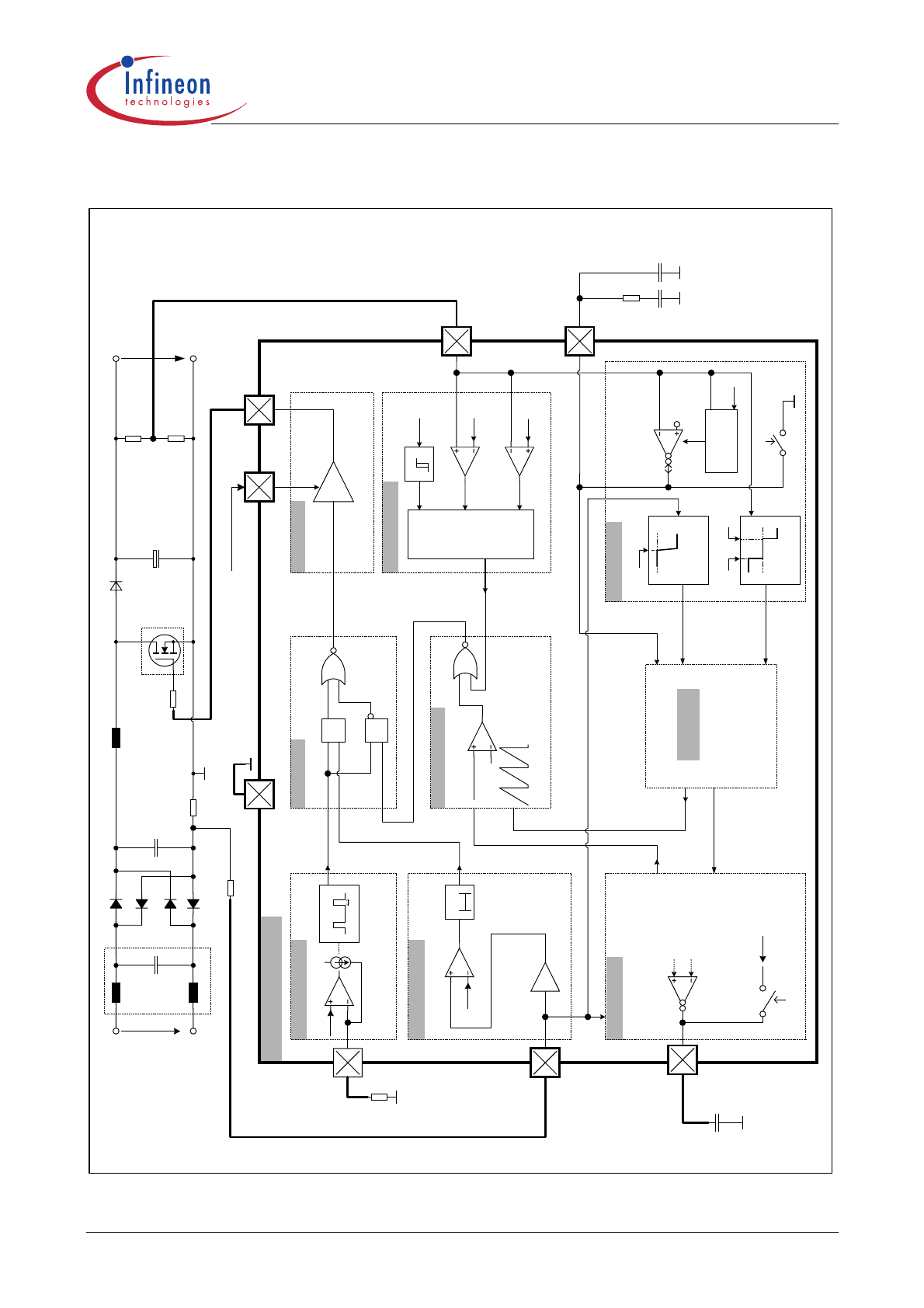
Representative Block diagram
Figure 2
Representative Block diagram
ICE1PCS01/G
8
5
...
26
5 VAC
Vo
ut
au
xil
iary
s
u
p
p
ly
30
0n
s
C2
1.
5V
-1.
43x
OT
A
3
2.
5V
ISENSE
GAT
E
VS
ENSE
VC
C
FR
EQ
C1
VCOMP
OT
A
2
IC
OMP
4.
0V
Fault
UVLO
VCC
0.
8V
GND
PWM
Com
par
ator
Ra
mp Ge
ne
rat
or
V
a
ri
ab
le
Osc
il
la
to
r
Tof
f m
in
O
ver
-cur
ren
t
Com
par
ator
D
e
gl
itch
er
PW
M Lo
gi
c
Gate
Drive
r
under
volt
age lockout
open-
lo
o
p
pr
ot
ect
Vol
tag
e
Loo
p
Cur
rent
Loop
Com
pensat
io
n
Prot
ec
tion
Bl
oc
k
2.
5V
out
put
uv pr
ot
e
c
t
P
e
a
k
C
u
rr
e
nt
Li
mi
t
Curre
nt Lo
op
Non
lin
ea
r
Gain
C3
C4
OT
A
1
5V
+
/-
30uA,
4
2uS
1.
1m
S
+
/-50u
A li
near
r
ange
R1
R5
L1
C2
R3
R4
C3
C5
C4
R6
R2
S2
Vin
D1
Fault
4.
75V
5.
25V
0.
73 V
0
-ve
Wi
nd
ow D
e
te
ct
+v
e
0
-ve
Sof
t Ove
r
Cur
re
nt
Cont
ro
l
4.
0V
S1
Fault
Soft
St
art
OP
1
Cur
rent
Sense
Opam
p
O
S
C CL
K
250n
s
R
S
R
S
Prot
ecti
on
Logi
c
C1
RF
I F
ilt
er
D2
...
D5
R7
CCM-PFC
ICE1PCS01/G
Functional Description
Version 1.2
7
06 Feb 2007
3.1
General
The ICE1PCS01/G is a 8 pin control IC for power factor
correction converters. It comes in both DIP and DSO
packages and is suitable for wide range line input
applications from 85 to 265 VAC. The IC supports
converters in boost topology and it operates in
continuous conduction mode (CCM) with average
current control.
The IC operates with a cascaded control; the inner
current loop and the outer voltage loop. The inner
current loop of the IC controls the sinusoidal profile for
the average input current. It uses the dependency of
the PWM duty cycle on the line input voltage to
determine the corresponding input current. This means
the average input current follows the input voltage as
long as the device operates in CCM. Under light load
condition, depending on the choke inductance, the
system may enter into discontinuous conduction mode
(DCM). In DCM, the average current waveform will be
distorted but the resultant harmonics are still low
enough to meet the Class D requirement of IEC 1000-
3-2.
The outer voltage loop controls the output bus voltage.
Depending on the load condition, OTA1 establishes an
appropriate voltage at VCOMP pin which controls the
amplitude of the average input current.
The IC is equipped with various protection features to
ensure safe operating condition for both the system
and device. Important protection features are namely
Brown-out protection, Current Limitation and Output
Under-voltage Protection.
3.2
Power Supply
An internal under voltage lockout (UVLO) block
monitors the VCC power supply. As soon as it exceeds
11.2V and the voltage at pin 6 (VSENSE) is >0.8V, the
IC begins operating its gate drive and performs its Soft-
Start as shown in Figure 3.
.
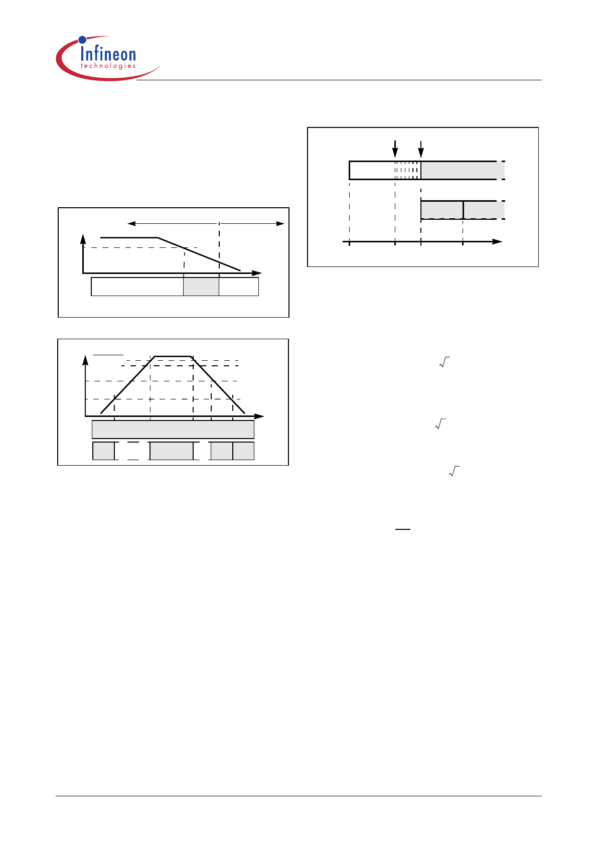
Figure 3
State of Operation respect to VCC
If VCC drops below 10.2V, the IC is off. The IC will then
be consuming typically 200
µA, whereas consuming
18mA during normal operation.
The IC can be turned off and forced into standby mode
by pulling down the voltage at pin 6 (VSENSE) to lower
than 0.8V. The current consumption is reduced to 3mA
in this mode.
3.3
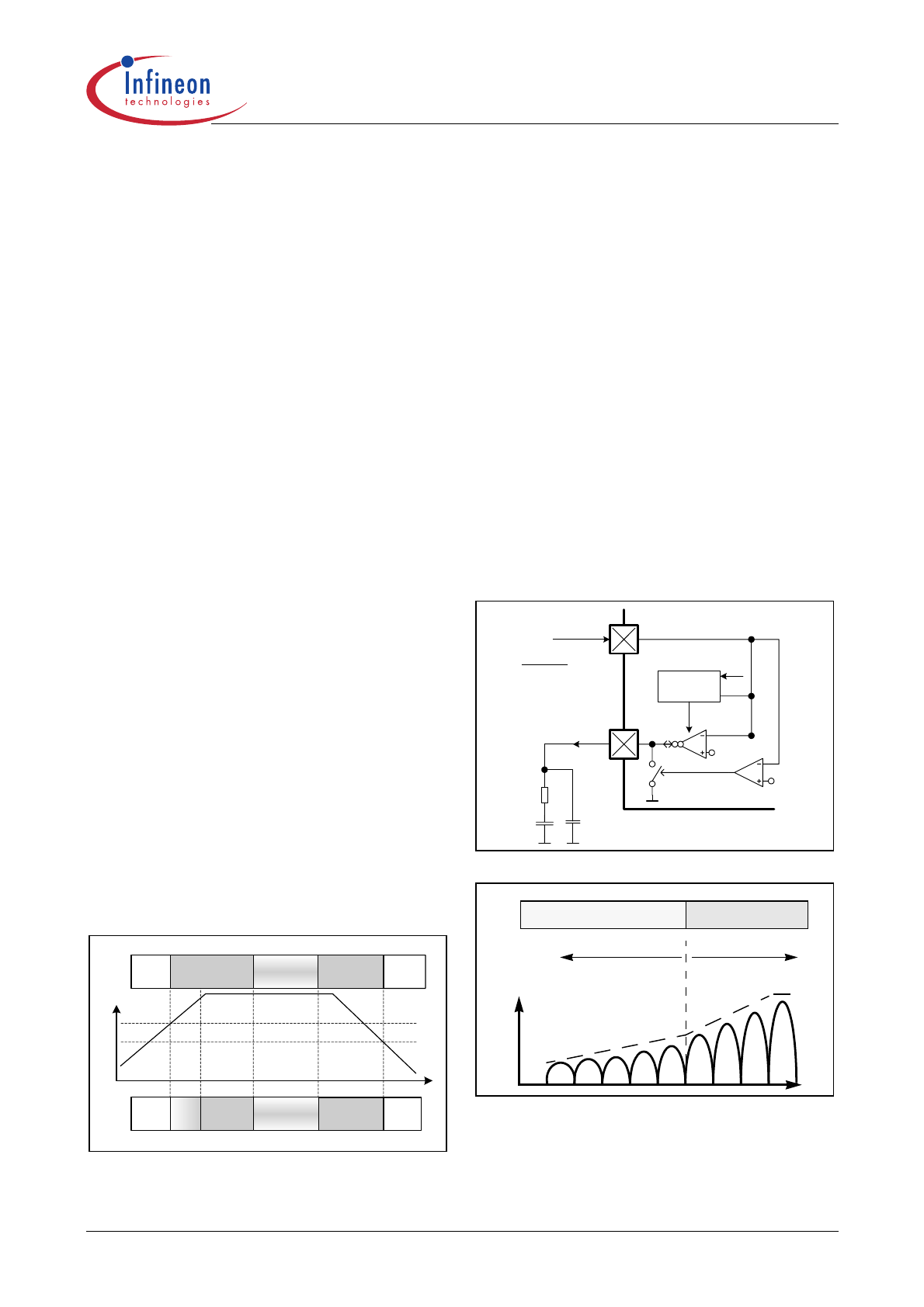
Start-up (Soft-Start)
Figure 4 and 5 show the operation of OTA1 during
startup. It sources a constant 10.8
µA into the
compensation network at pin 5 (VCOMP). The voltage
at this pin rises linearly and so does the amplitude of
the input current. As soon as the output voltage V
OUT
reaches 80% of its rated level, the startup procedure is
finished and the normal voltage control takes over. In
normal operation, the IC operates with a higher
maximum current at OTA1 and therefore with a higher
voltage loop gain in order to improve the dynamic
behavior of the device.
.
Figure 4
Soft Start Circuit
Figure 5
Soft Start with controlled current
The advantage of this technique is a soft-start function
with lower stress for the boost diode but without the risk
of audible noise.
V
CC
V
VSENSE
> 0,8 V
V
VSENSE
< 0,8 V
11.2 V
10.5 V
t
OFF
Soft
start
Open loop/
Standby
Normal
Operation
IC's
State
OFF
V
VSENSE
> 0,8 V
Normal
Operation
VCOMP
C5
C4
VSENSE
OTA1
5V
ICE1PCS01/G
C3
Open-Loop
Protect
(OLP)
0.8V
R3 + R4
R4
x V
OUT
)
(
10.8uA during
Soft Start
R6
S1
4.0V
Soft Start
Soft Start
Normal Operation
av(I
IN
)
V
OUT
< 80% rated
V
OUT
> 80% rated
t
3
Functional Description
CCM-PFC
ICE1PCS01/G
Functional Description
Version 1.2
8
06 Feb 2007
3.4
System Protection
The IC provides several protection features in order to
ensure the PFC system in safe operating range.
Depending on the input line voltage (V
IN
) and output
bus voltage (V
OUT
), Figure 6 and 7 show the conditions
when these protections are active.
Figure 6
V
IN
Related Protection Features
Figure 7
V
OUT
Related Protection Features
The following sections describe the functionality of
these protection features.
3.4.1
Brown-Out Protection (BOP)
Brown-out occurs when the input voltage V
IN
falls below
the minimum input voltage of the design (i.e. 85V for
universal input voltage range) and the VCC has not
entered into the V
CCUVLO
level yet. For a system without
BOP, the boost converter will increasingly draw a
higher current from the mains at a given output power
which may exceed the maximum design values of the
input current. The ICE1PCS01/G limits internally the
current drawn from the mains and therefore also limits
the input power. The difference of input and output
power will result in decreasing output voltage. If the
condition prolongs, the decreasing V
OUT
will terminate
in output under voltage condition (OUV, 50% of rated),
and the IC will be shut down (See section 3.4.5).
Figure 8 shows the occurrence of BOP in respect to the
ISENSE voltage.
Figure 8
BOP, SOC and PCL Protection as function
of V
ISENSE
The V
IN
threshold for BOP to occur is dependent on the
voltage at ISENSE and thus the output power. The
rated output power with a minimum V
IN
(V
INMIN
) is
Due to the internal parameter tolerance, the maximum
power with V
INMIN
before BOP occurs is
And the BOP takes over the normal operation under
rated output power latest at an input voltage of
3.4.2
Soft Over Current Control (SOC)
The IC is designed not to support any output power
that corresponds to a voltage lower than -0.73V at the
ISENSE pin. A further increase in the inductor current,
which results in a lower ISENSE voltage, will activate
the Soft Over Current Control (SOC). This is a soft
control as it does not directly switch off the gate drive
like the PCL. It acts on the nonlinear gain block to result
in a reduced PWM duty cycle.
3.4.3
Peak Current Limit (PCL)
The IC provides a cycle by cycle peak current limitation
(PCL). It is active when the voltage at pin 3 (ISENSE)
reaches -1.08V. This voltage is amplified by OP1 by a
factor of -1.43 and connected to comparator C2 with a
reference voltage of 1.5V as shown in Figure 9. A
deglitcher with 300ns after the comparator improves
noise immunity to the activation of this protection.
t
V
INMIN
(1)
V
IN
(VAC)
VCC > V
CCUVLO
Normal
Operation
IC OFF
BOP
VCC<V
CCUVLO
(1)
V
INMIN
where BOP activates depends on the output power
IC’s
State
t
V
OUT
PCL / SOC
16%
50%
100%
OLP
OLP
OUV
105%
OVP
V
OUT,Rated
V
ISENSE
-0.6V -0.73V
-1.08V
Normal
Operation
SOC
PCL
P
OUT
(rated)
BOP
IC’s
State
0
(BOP occurs at V
ISENSE
= -0.6V Max)
P
OUT
(max)
P
OUT
rated
(
)
V
INMIN
0.6
R1
2
⋅
-------------------
×
=
P
OUT
max
(
)
V
INMIN
0.73
R1
2
⋅
-------------------
×
=
V
BOPMAX
P
OUT
rated
(
) R1
2
⋅
0.73
-------------------
×
=
CCM-PFC
ICE1PCS01/G
Functional Description
Version 1.2
9
06 Feb 2007
Figure 9
Peak Current Limit (PCL)
3.4.4
Open Loop Protection / Input Under
Voltage Protect (OLP)
Whenever VSENSE voltage falls below 0.8V, or
equivalently V
OUT
falls below 16% of its rated value, it
indicates an open loop condition (i.e. VSENSE pin not
connected) or an insufficient input voltage V
IN
for
normal operation. In this case, most of the blocks within
the IC will be shutdown. It is implemented using
comparator C3 with a threshold of 0.8V as shown in the
IC block diagram in Figure 2.
3.4.5
Output Under Voltage Detection (OUV)
In the event of main interrupt or brown-out condition,
the PFC system is not able to deliver the rated output
power. This will cause the output voltage V
OUT
to drop
below its rated value. The IC provides an output under
voltage detection that checks if V
OUT
is falling below
50% of its rated value. Comparator C4 as shown in the
device block diagram (Figure 2) senses the voltage at
pin 6 (VSENSE) with a reference of 2.5V. If comparator
C4 trips, the IC will be shut down as in OLP. The IC will
be ready to restart if there is sufficient V
IN
to pull V
OUT
out of OLP.
3.4.6
Over-Voltage Protection (OVP)
Whenever V
OUT
exceeds the rated value by 5%, the
over-voltage protection OVP is active as shown in
Figure 7. This is implemented by sensing the voltage at
pin VSENSE with respect to a reference voltage of
5.25V. A VSENSE voltage higher than 5.25V will
immediately reduce the output duty cycle, bypassing
the normal voltage loop control. This results in a lower
input power to reduce the output voltage V
OUT
.
3.5
Frequency Setting
The switching frequency of the PFC converter can be
set with an external resistor R5 at FREQ pin. The pin
voltage V
FREQ
is typically 2.5V. The corresponding
capacitor for the oscillator is integrated in the device
and the R5/frequency relationship is given at the
“Electrical Characteristic” section. The
recommended operating frequency range is from
50kHz to 250kHz. As an example, a R5 of 33k
Ω at pin
FREQ will set a switching frequency F
SW
of 133kHz
typically.
3.6
Average Current Control
3.6.1
Complete Current Loop
The complete system current loop is shown in Figure
10.
Figure 10 Complete System Current Loop
It consists of the current loop block which averages the
voltage at pin ISENSE, resulted from the inductor
current flowing across R1. The averaged waveform is
compared with an internal ramp in the ramp generator
and PWM block. Once the ramp crosses the average
waveform, the comparator C1 turns on the driver stage
through the PWM logic block. The Nonlinear Gain block
defines the amplitude of the inductor current. The
following sections describe the functionality of each
individual blocks.
3.6.2
Current Loop Compensation
The compensation of the current loop is done at the
ICOMP pin. This is the OTA2 output and a capacitor C3
has to be installed at this node to ground (see Figure
10). Under normal mode of operation, this pin gives a
voltage which is proportional to the averaged inductor
current. This pin is internally shorted to 5V in the event
of IC shuts down when OLP and UVLO occur.
3.6.3
Pulse Width Modulation (PWM)
The IC employs an average current control scheme in
continuous conduction mode (CCM) to achieve the
power factor correction.
ISENSE
ICE1PCS01/G
R1
R2
I
INDUCTOR
OP1
1.43x
Current Limit
300ns
C2
Deglitcher
Turn Off
Driver
1.5V
Full-wave
Rectifier
R
S
ICE1PCS01/G
Vout
L1
C2
R3
R4
Gate
Driver
D1
From
Full-wave
Retifier
GATE
R1
R2
OTA2
ICOMP
4V
Current Loop
Compensation
Current Loop
Nonlinear
Gain
1.1mS
+/-50uA (linear range)
C3
S2
Fault
ISENSE
C1
PWM
Comparator
PWM Logic
Q
Input From
Voltage Loop
voltage
proportional to
averaged
Inductor current
R7
CCM-PFC
ICE1PCS01/G
Functional Description
Version 1.2
10
06 Feb 2007
Assuming the voltage loop is working and output
voltage is kept constant, the off duty cycle D
OFF
for a
CCM PFC system is given as
From the above equation, D
OFF
is proportional to V
IN
.
The objective of the current loop is to regulate the
average inductor current such that it is proportional to
the off duty cycle D
OFF
, and thus to the input voltage
V
IN
. Figure 11 shows the scheme to achieve the
objective.
Figure 11 Average Current Control in CCM
The PWM is performed by the intersection of a ramp
signal with the averaged inductor current at pin 5
(ICOMP). The PWM cycle starts with the Gate turn off
for a duration of T
OFFMIN
(250ns typ.) and the ramp is
kept discharged. The ramp is then allowed to rise after
T
OFFMIN
expires. The off time of the boost transistor
ends at the intersection of the ramp signal and the
averaged current waveform. This results in the
proportional relationship between the average current
and the off duty cycle D
OFF
.
Figure 12 shows the timing diagrams of T
OFFMIN
and the
PWM waveforms.
Figure 12 Ramp and PWM waveforms
3.6.4
Nonlinear Gain Block
The nonlinear gain block controls the amplitude of the
regulated inductor current. The input of this block is the
voltage at pin VCOMP. This block has been designed
to support the wide input voltage range (85-265VAC).
3.7
PWM Logic
The PWM logic block prioritizes the control input
signals and generates the final logic signal to turn on
the driver stage. The speed of the logic gates in this
block, together with the width of the reset pulse T
OFFMIN
,
are designed to meet a maximum duty cycle D
MAX
of
95% at the GATE output under 133kHz of operation.
In case of high input currents which result in Peak
Current Limitation, the GATE will be turned off
immediately and maintained in off state for the current
PWM cycle. The signal Toffmin resets (highest priority,
overriding other input signals) both the current limit
latch and the PWM on latch as illustrated in Figure 13.
Figure 13 PWM Logic
3.8
Voltage Loop
The voltage loop is the outer loop of the cascaded
control scheme which controls the PFC output bus
voltage V
OUT
. This loop is closed by the feedback
sensing voltage at VSENSE which is a resistive divider
tapping from V
OUT
. The pin VSENSE is the input of
OTA1 which has an internal reference of 5V. Figure 14
shows the important blocks of this voltage loop.
3.8.1
Voltage Loop Compensation
The compensation of the voltage loop is installed at the
VCOMP pin (see Figure 14). This is the output of OTA1
and the compensation must be connected at this pin to
ground. The compensation is also responsible for the
soft start function which controls an increasing AC input
current during start-up.
D
OFF
V
IN
V
OUT
--------------
=
t
ave(I
IN
) at ICOMP
ramp profile
GATE
drive
T
OFFMIN
250ns
V
CREF
(1)
V
RAMP
PWM
ramp
released
PWM cycle
(1)
V
CREF
is a function of V
ICOMP
t
G1
R
S
L1
R
S
L2
Peak Current
Limit
Current Loop
PWM on signal
Toffmin
250ns
Current
Limit Latch
PWM on
Latch
HIGH =
turn GATE on
Q
Q