
February, 10
th
2012
Automotive grade
AUIPS7145R
www.irf.com
1
CURRENT SENSE HIGH SIDE SWITCH
Features
Suitable for 24V systems
Over current shutdown
Over temperature shutdown
Current sensing
Active clamp
Reverse circulation immunization
Low current
ESD protection
Optimized Turn On/Off for EMI
Applications
21W Filament lamp
Solenoid
24V loads for trucks
Description
The AUIPS7145R is a fully protected four terminal high
side switch specifically designed for driving lamp. It
features current sensing, over-current, over-temperature,
ESD protection and drain to source active clamp. The Ifb
pin is used for current sensing. The over-current shutdown
is higher than inrush current of the lamp.
Product Summary
Rds(on) 100m
max.
Vclamp 65V
Current shutdown 20A min.
Packages
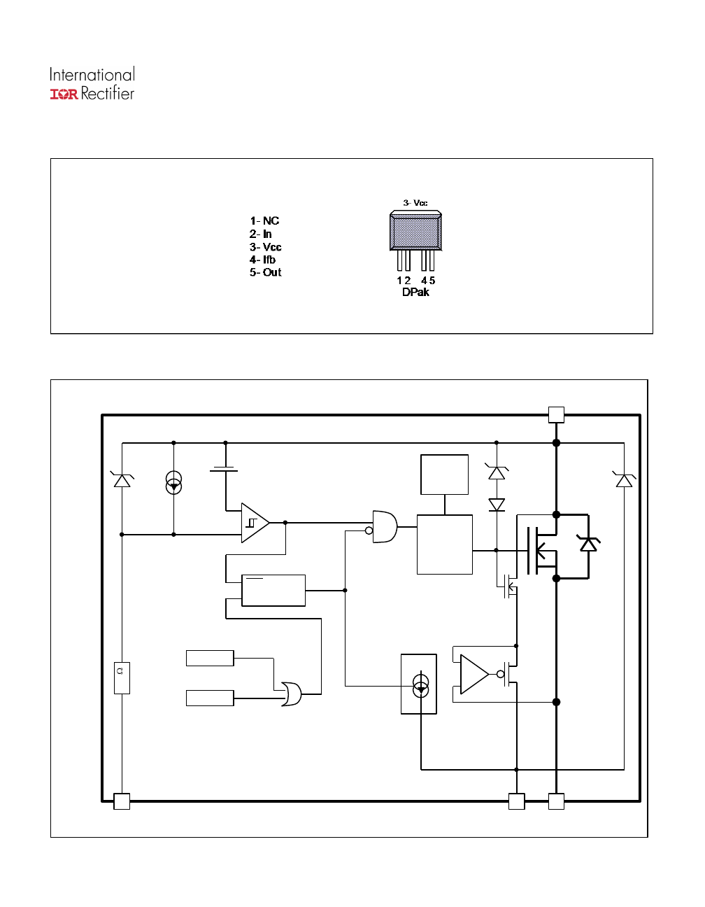
DPak
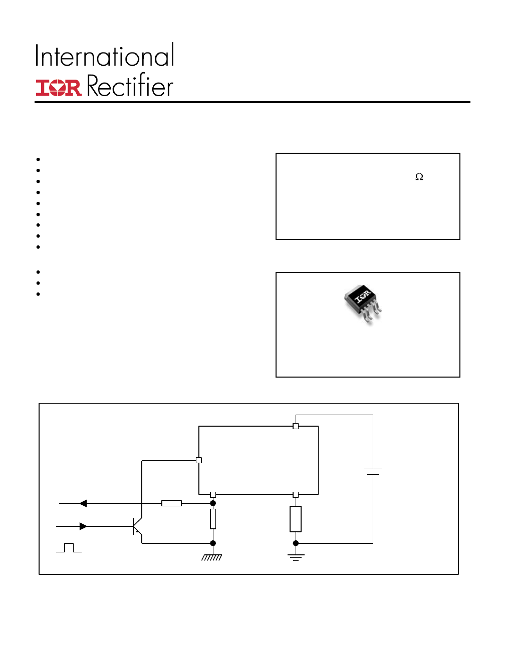
Typical Connection
Out
IPS
IN
2.5k
Vcc
Load
Battery
Input
Power
Ground
Ifb
Logic
Ground
Current feeback
10k
On
Off
AUIPS7145R
www.irf.com
2
Qualification Information
†
Qualification Level
Automotive
(per AEC-Q100
††
)
Comments: This family of ICs has passed an Automotive qualification.
IR’s
Industrial and Consumer qualification level is granted by extension of the
higher Automotive level.
Moisture Sensitivity Level
DPAK-5L
MSL1,
260°C
(per IPC/JEDEC J-STD-020)
ESD
Machine Model
Class M2 (200 V)
(per AEC-Q100-003)
Human Body Model
Class H1C (1500 V)
(per AEC-Q100-002)
Charged Device Model
Class C5 (1000 V)
(per AEC-Q100-011)
IC Latch-Up Test
Class II, Level A
(per AEC-Q100-004)
RoHS Compliant
Yes
†
Qualification standards can be found at International Rectifier’s web site
http://www.irf.com/
††
Exceptions to AEC-Q100 requirements are noted in the qualification report.
AUIPS7145R
www.irf.com
3
Absolute Maximum Ratings
Absolute maximum ratings indicate sustained limits beyond which damage to the device may occur. (Tj= -40°C..150°C,
Vcc=6..50V unless otherwise specified).
Symbol
Parameter
Min.
Max.
Units
Vout
Maximum output voltage
Vcc-60 Vcc+0.3
V
I rev
Maximum reverse pulsed current (t=100µs) see page 8
30
A
Isd cont.
Maximum diode continuous current Tambient=25°C, Rth=70°C/W
2.3
Vcc-Vin max. Maximum Vcc voltage
-16
60
V
Iifb, max.
Maximum feedback current
-50
10
mA
Vcc sc.
Maximum Vcc voltage with short circuit protection see page 8
50
V
Pd
Maximum power dissipation (internally limited by thermal protection)
W
Rth=50°C/W DPack 6cm² footprint
2.5
Tj max.
Maximum operating junction temperature
-40
150
°C
Maximum storage junction temperature
-55
150
Thermal Characteristics
Symbol
Parameter
Typ.
Max.
Units
Rth1
Thermal resistance junction to ambient DPak Std footprint
70
°C/W
Rth2
Thermal resistance junction to ambient Dpak 6cm² footprint
50
Rth3
Thermal resistance junction to case Dpak
4
Recommended Operating Conditions
These values are given for a quick design.
Symbol
Parameter
Min.
Max.
Units
Iout
Continuous output current, Tambient=85°C, Tj=125°C
A
Rth=50°C/W, Dpak 6cm² footprint
2.1
RIfb
Ifb resistor
1.5
k
AUIPS7145R
www.irf.com
4
Static Electrical Characteristics
Tj=-40°C..150°C, Vcc=6-50V (unless otherwise specified)
Symbol
Parameter
Min.
Typ.
Max.
Units
Test Conditions
Vcc op.
Operating voltage
6
60
V
Rds(on)
ON state resistance Tj=25°C
75
100
m
Ids=2A
ON state resistance Tj=150°C(2)
135
180
Icc off
Supply leakage current
1
3
µA
Vin=Vcc / Vifb=Vgnd
Vout=Vgnd, Tj=25°C
Iout off
Output leakage current
1
3
I in on
Input current while on
0.6
2
4
mA
Vcc-Vin=28V, Tj=25°C
V clamp1
Vcc to Vout clamp voltage 1
60
64
V
Id=10mA
V clamp2
Vcc to Vout clamp voltage 2
60
65
72
Id=6A see fig. 2
Vih(1)
High level Input threshold voltage
3
5
Id=10mA
Vil(1)
Low level Input threshold voltage
1.5
2.3
4.7
Vf
Forward body diode voltage Tj=25°C
0.8
0.9
If=1A
Forward body diode voltage Tj=125°C
0.65
0.75
(1) Input thresholds are measured directly between the input pin and the tab.
Switching Electrical Characteristics
Vcc=28V, Resistive load=27 , Tj=25°C
Symbol
Parameter
Min.
Typ. Max.
Units
Test Conditions
tdon
Turn on delay time to 20%
4
10
20
µs
See fig. 1
tr
Rise time from 20% to 80% of Vcc
2
5
10
tdoff
Turn off delay time
20
40
80
µs
tf
Fall time from 80% to 20% of Vcc
2.5
5
10
Protection Characteristics
Tj=-40°C..150°C, Vcc=6-50V (unless otherwise specified)
Symbol
Parameter
Min. Typ. Max.
Units
Test Conditions
Tsd
Over temperature threshold
150(2)
165
°C
See fig. 3 and fig.11
Isd
Over-current shutdown
20
25
35
A
See fig. 3 and page 7
I fault
Ifb after an over-current or an over-
temperature (latched)
2.2
3
5
mA
See fig. 3
Current Sensing Characteristics
Tj=-40°C..150°C, Vcc=6-50V (unless otherwise specified). Specified 500µs after the turn on. Vcc-Vifb>4V
Symbol
Parameter
Min. Typ. Max.
Units
Test Conditions
Ratio
I load / Ifb current ratio
2000
2400
2800
Iout<4A
Ratio_TC
I load / Ifb variation over temperature(2)
-5%
0
+5
%
Tj=-40°C to +150°C
I offset
Load current offset
-0.02
0
0.02
A
Iout<4A
Ifb leakage
Ifb leakage current On in open load
0
1
10
µA
Iout=0A, Vcc-Vin=28V
(2) Guaranteed by design
AUIPS7145R
www.irf.com
5
Lead Assignments
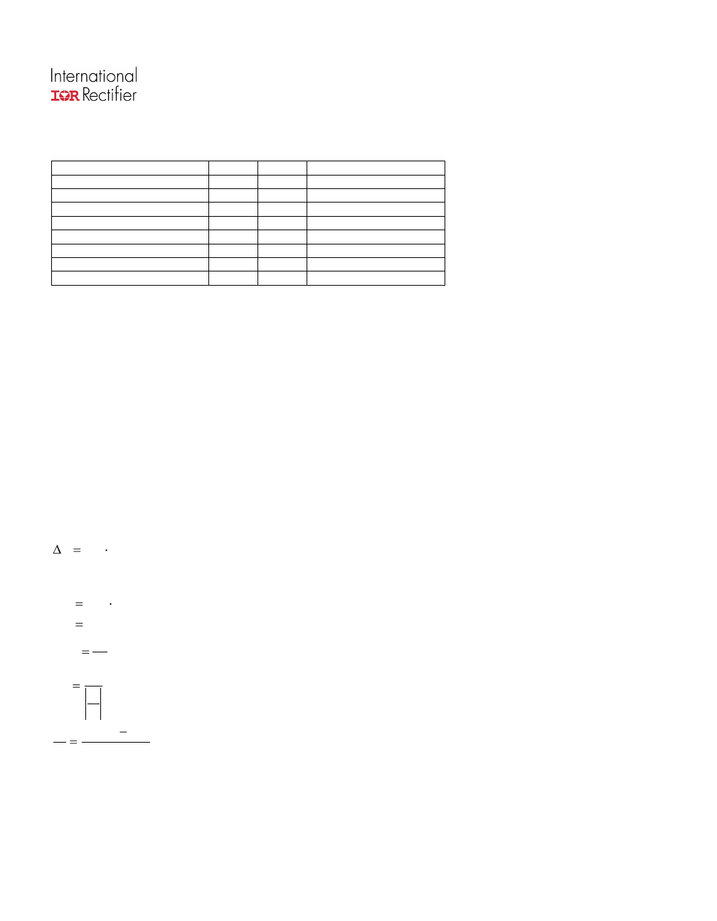
Functional Block Diagram
All values are typical
Diag
Charge
Pump
Driver
IFB OUT
VCC
75V
100
Tj > 165°C
Iout > 25A
60V
75V
-
+
75V
IN
Set
Reset
Latch
Q
1.5mA
+
-
3V
AUIPS7145R
www.irf.com
6
Truth Table
Op. Conditions
Input
Output
Ifb pin voltage
Normal mode
H
L
0V
Normal mode
L
H
I load x Rfb / Ratio
Open load
H
L
0V
Open load
L
H
0V
Short circuit to GND
H
L
0V
Short circuit to GND
L
L
V fault (latched)
Over temperature
H
L
0V
Over temperature
L
L
V fault (latched)
Operating voltage
Maximum Vcc voltage : this is the maximum voltage before the breakdown of the IC process.
Operating voltage : This is the Vcc range in which the functionality of the part is guaranteed. The AEC-Q100 qualification
is run at the maximum operating voltage specified in the datasheet.
Reverse battery
During the reverse battery the Mosfet is kept off and the load current is flowing into the body diode of the power Mosfet.
Power dissipation in the IPS : P = I load * Vf
There is no protection, so Tj must be lower than 150°C in the worst case condition of current and ambient temperature.
If the power dissipation is too high in Rifb, a diode in serial can be added to block the current.
The transistor used to pull-down the input should be a bipolar in order to block the reverse current. The 100ohm input
resistor can not sustain continuously 16V (see Vcc-Vin max. in the Absolute Maximum Ratings section)
Active clamp
The purpose of the active clamp is to limit the voltage across the MOSFET to a value below the body diode break down
voltage to reduce the amount of stress on the device during switching.
The temperature increase during active clamp can be estimated as follows:
)
t
(
Z
P
CLAMP
TH
CL
Tj
Where:
)
t
(
Z
CLAMP
TH
is the thermal impedance at t
CLAMP
and can be read from the thermal impedance curves given in the
data sheets.
CLavg
CL
CL
I
V
P
: Power dissipation during active clamp
65V
V
CL
: Typical V
CLAMP
value.
2
I
I
CL
CLavg
: Average current during active clamp
dt
di
I
t
CL
CL
: Active clamp duration
L
V
V
dt
di
CL
Battery
: Demagnetization current
Figure 9 gives the maximum inductance versus the load current in the worst case : the part switches off after an over
temperature detection. If the load inductance exceeds the curve, a free wheeling diode is required.
AUIPS7145R
www.irf.com
7
Over-current protection
The threshold of the over-current protection is set in order to guarantee that the device is able to turn on a load with an
inrush current lower than the minimum of Isd. Nevertheless for high current and high temperature the device may switch
off for a lower current due to the over-temperature protection. This behavior is shown in Figure 11.
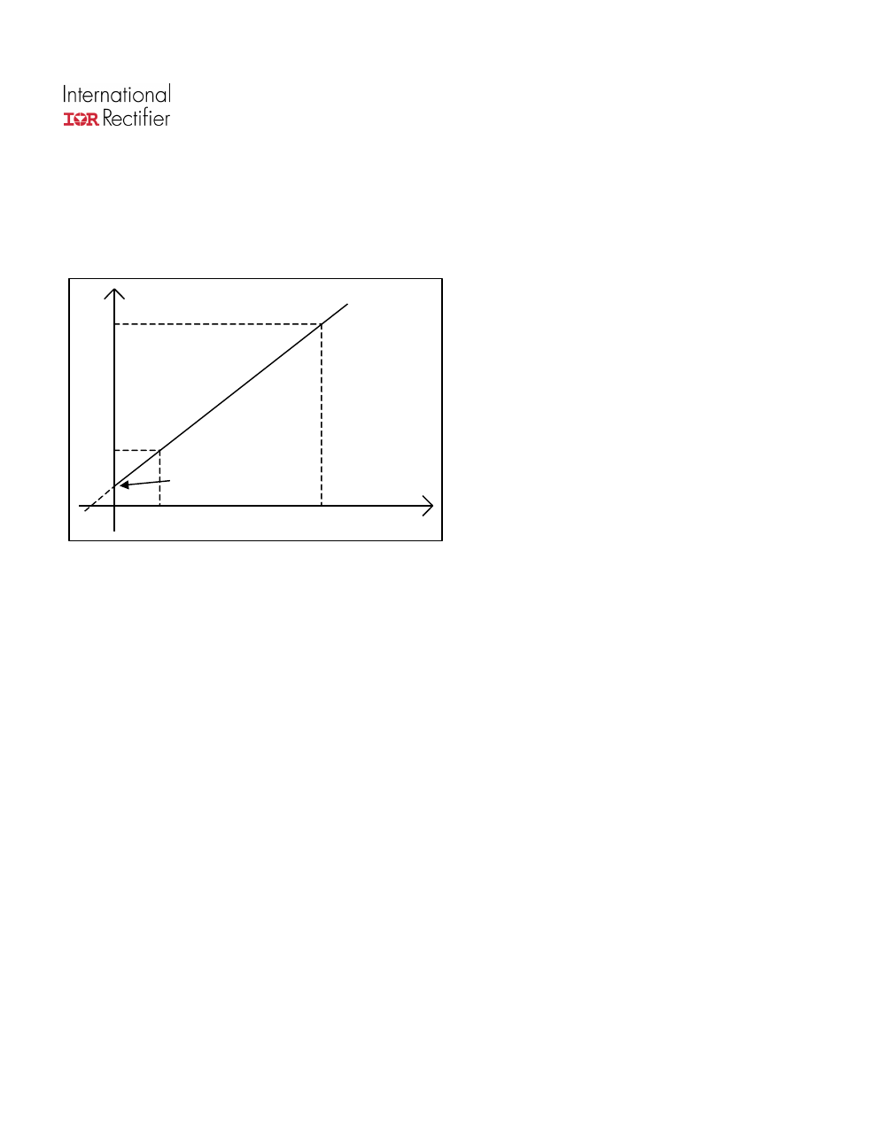
Current sensing accuracy
Iout
Ifb
Ifb leakage
Ifb2
Ifb1
Iout2
Iout1
I offset
The current sensing is specified by measuring 3 points :
- Ifb1 for Iout1
- Ifb2 for Iout2
- Ifb leakage for Iout=0
The parameters in the datasheet are computed with the following formula :
Ratio = ( Iout2
– Iout1 )/( Ifb2 – Ifb1)
I offset = Ifb1 x Ratio
– Iout1
This allows the designer to evaluate the Ifb for any Iout value using :
Ifb = ( Iout + I offset ) / Ratio if Ifb > Ifb leakage
For some applications, a calibration is required. In that case, the accuracy of the system will depends on the variation of
the I offset and the ratio over the temperature range. The ratio variation is given by Ratio_TC specified in page 4.
The Ioffset variation depends directly on the Rdson :
I offset@-40°C= I offset@25°C / 0.8
I offset@150°C= I offset@25°C / 1.9
AUIPS7145R
www.irf.com
8
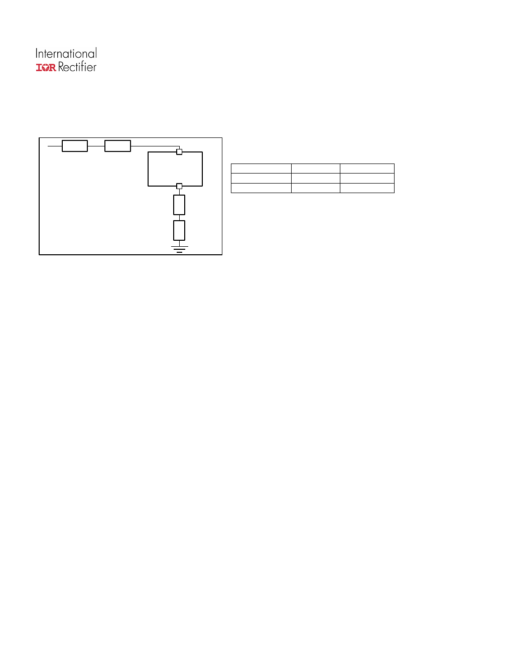
Maximum Vcc voltage with short circuit protection
The maximum Vcc voltage with short circuit is the maximum voltage for which the part is able to protect itself under test
conditions representative of the application. 2 kind of short circuits are considered : terminal and load short circuit.
Maximum current during reverse circulation
In case of short circuit to battery, a voltage drop of the Vcc may create a current which circulate in reverse mode. When
the device is on, this reverse circulation current will not trigger the internal fault latch. This immunization is also true when
the part turns on while a reverse current flows into the device. The maximum current (I rev) is specified in the maximum
rating section.
L SC
R SC
Terminal SC
0.1 µH
10 mohm
Load SC
10 µH
100 mohm
Out
IPS
Vcc
L SC
L supply
5µH
R supply
10mohm
R SC
AUIPS7145R
www.irf.com
9
Tj
Tsd
165°C
Ids
Vin
I shutdown
Tshutdown
Vifb
V fault
Figure 3
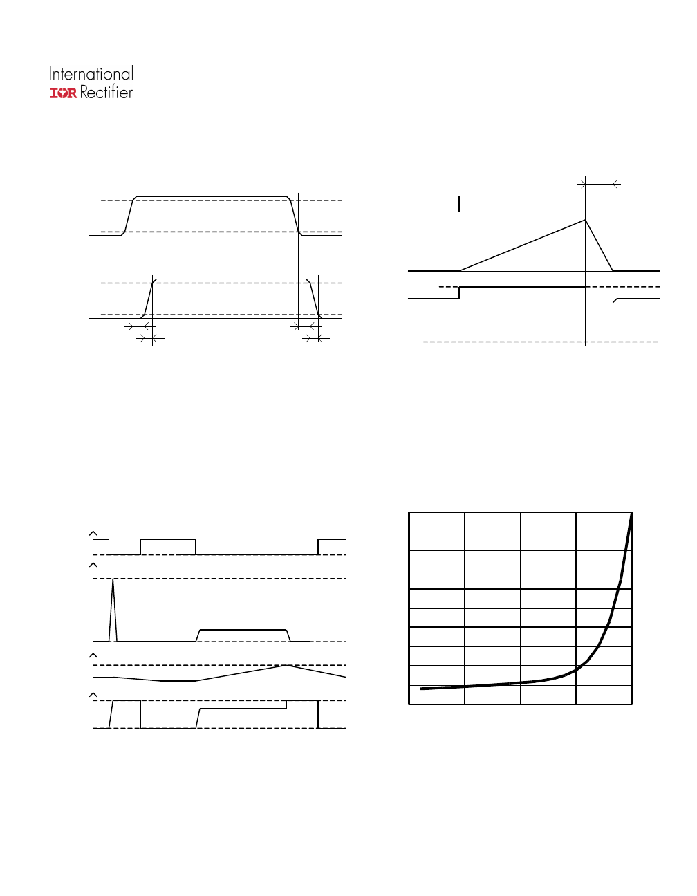
– Protection timing diagram
Figure 1
– IN rise time & switching definitions
Vds
Ids
Vcc-Vin
Vcc
Vds clamp
T clamp
See Application Notes to evaluate power dissipation
Figure 2
– Active clamp waveforms
0
2
4
6
8
10
-50
0
50
100
150
Tj, junction temperature (°C)
Figure 4
– Icc off (µA) Vs Tj (°C)
Ic
c
o
ff
,
s
u
p
p
ly
lea
k
a
g
e
c
u
rr
e
n
t
(µ
A
)
Vout
Vcc-Vin
80%
20%
80%
20%
Td on
Tr
Td off
Tf
AUIPS7145R
www.irf.com
10
Figure 8
– Transient thermal impedance (°C/W)
Vs time (s)
Zt
h
,
tr
a
n
s
ien
t
th
e
rmal
im
p
e
d
a
n
c
e
(
°C/W)
Time (s)
50%
100%
150%
200%
-50
0
50
100
150
R
d
s
(o
n
),
D
ra
in
-to
-S
o
u
rc
e
On
R
e
s
is
ta
n
c
e
(N
o
rmaliz
e
d
)
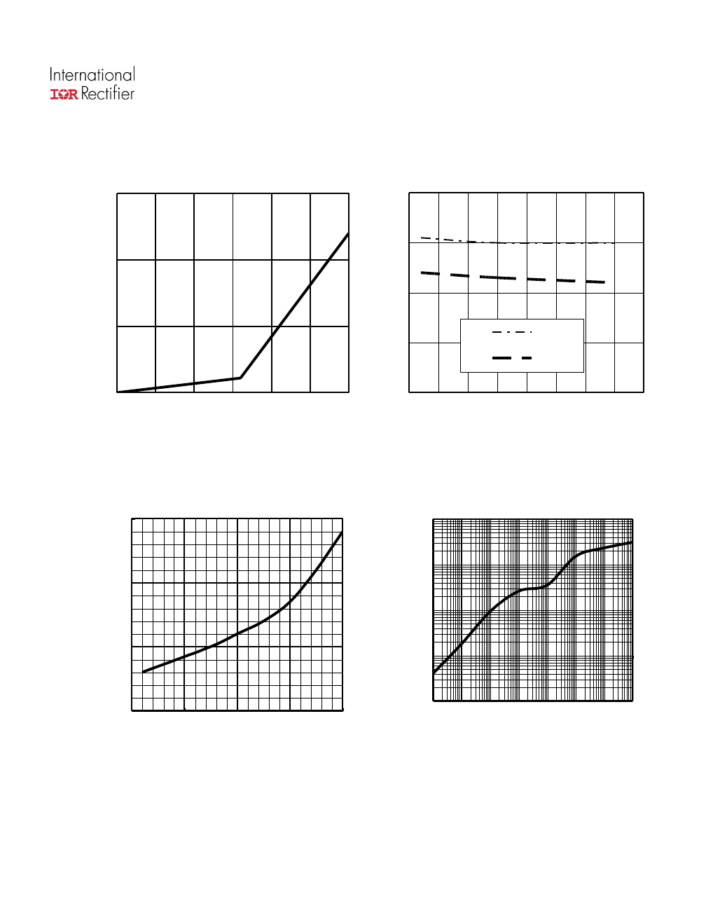
Figure 7 - Normalized Rds(on) (%) Vs Tj (°C)
Tj, junction temperature (°C)
0
1
2
3
4
-50
-25
0
25
50
75
100
125
150
VIH
VIL
Tj, junction temperature (°C)
V
ih
a
n
d
V
il
(V
)
Figure 6
– Vih and Vil (V) Vs Tj (°C)
Figure 5
– Icc off (µA) Vs Vcc-Vout (V)
Vcc-Vout, supply voltage (V)
Ic
c
,
s
u
p
p
ly
c
u
rr
e
n
t
(µ
A)
0.01
0.10
1.00
10.00
100.00
1.E-
05
1.E-
04
1.E-
03
1.E-
02
1.E-
01
1.E+0
0
1.E+0
1
1.E+0
2
0
5
10
15
0
10
20
30
40
50
60