

TLE 8444SL
Quad Half-Bridge Driver IC
Data Sheet, Rev. 1.1, July 2009
Automotive Power

Data Sheet
2
Rev. 1.1, 2009-07-07
TLE 8444SL
Table of Contents
1
Overview . . . . . . . . . . . . . . . . . . . . . . . . . . . . . . . . . . . . . . . . . . . . . . . . . . . . . . . . . . . . . . . . . . . . . . . 3
2
Block Diagram . . . . . . . . . . . . . . . . . . . . . . . . . . . . . . . . . . . . . . . . . . . . . . . . . . . . . . . . . . . . . . . . . . . 4
3
Pin Configuration . . . . . . . . . . . . . . . . . . . . . . . . . . . . . . . . . . . . . . . . . . . . . . . . . . . . . . . . . . . . . . . . 6
3.1
Pin Assignment . . . . . . . . . . . . . . . . . . . . . . . . . . . . . . . . . . . . . . . . . . . . . . . . . . . . . . . . . . . . . . . . . . . 6
3.2
Pin Definitions and Functions . . . . . . . . . . . . . . . . . . . . . . . . . . . . . . . . . . . . . . . . . . . . . . . . . . . . . . . . 6
4
General Product Characteristics . . . . . . . . . . . . . . . . . . . . . . . . . . . . . . . . . . . . . . . . . . . . . . . . . . . . 8
4.1
Absolute Maximum Ratings . . . . . . . . . . . . . . . . . . . . . . . . . . . . . . . . . . . . . . . . . . . . . . . . . . . . . . . . . 8
4.2
Functional Range . . . . . . . . . . . . . . . . . . . . . . . . . . . . . . . . . . . . . . . . . . . . . . . . . . . . . . . . . . . . . . . . . 9
4.3
Thermal Resistance . . . . . . . . . . . . . . . . . . . . . . . . . . . . . . . . . . . . . . . . . . . . . . . . . . . . . . . . . . . . . . . 9
4.4
Electrical Characteristics . . . . . . . . . . . . . . . . . . . . . . . . . . . . . . . . . . . . . . . . . . . . . . . . . . . . . . . . . . 10
5
Block Description . . . . . . . . . . . . . . . . . . . . . . . . . . . . . . . . . . . . . . . . . . . . . . . . . . . . . . . . . . . . . . . 12
5.1
Power Supply . . . . . . . . . . . . . . . . . . . . . . . . . . . . . . . . . . . . . . . . . . . . . . . . . . . . . . . . . . . . . . . . . . . 12
5.1.1
General . . . . . . . . . . . . . . . . . . . . . . . . . . . . . . . . . . . . . . . . . . . . . . . . . . . . . . . . . . . . . . . . . . . . . . 12
5.1.2
Sleep Mode . . . . . . . . . . . . . . . . . . . . . . . . . . . . . . . . . . . . . . . . . . . . . . . . . . . . . . . . . . . . . . . . . . . 12
5.1.3
Reverse Polarity . . . . . . . . . . . . . . . . . . . . . . . . . . . . . . . . . . . . . . . . . . . . . . . . . . . . . . . . . . . . . . . 13
5.2
Input / Output Stages . . . . . . . . . . . . . . . . . . . . . . . . . . . . . . . . . . . . . . . . . . . . . . . . . . . . . . . . . . . . . 14
5.3
Monitoring Functions . . . . . . . . . . . . . . . . . . . . . . . . . . . . . . . . . . . . . . . . . . . . . . . . . . . . . . . . . . . . . 16
5.3.1
Diagnostics . . . . . . . . . . . . . . . . . . . . . . . . . . . . . . . . . . . . . . . . . . . . . . . . . . . . . . . . . . . . . . . . . . . 16
5.3.2
Power Supply Monitoring . . . . . . . . . . . . . . . . . . . . . . . . . . . . . . . . . . . . . . . . . . . . . . . . . . . . . . . . . 17
5.3.3
Temperature Monitoring . . . . . . . . . . . . . . . . . . . . . . . . . . . . . . . . . . . . . . . . . . . . . . . . . . . . . . . . . 18
5.4
Power-Outputs 1-4 (Half Bridge Outputs) . . . . . . . . . . . . . . . . . . . . . . . . . . . . . . . . . . . . . . . . . . . . . . 19
5.4.1
Protection and Diagnosis . . . . . . . . . . . . . . . . . . . . . . . . . . . . . . . . . . . . . . . . . . . . . . . . . . . . . . . . . 19
5.4.1.1
Short Circuit of Output to Ground or Vs . . . . . . . . . . . . . . . . . . . . . . . . . . . . . . . . . . . . . . . . . . . . 19
5.4.1.2
Open Load . . . . . . . . . . . . . . . . . . . . . . . . . . . . . . . . . . . . . . . . . . . . . . . . . . . . . . . . . . . . . . . . . . 23
5.5
Output Switching Capability . . . . . . . . . . . . . . . . . . . . . . . . . . . . . . . . . . . . . . . . . . . . . . . . . . . . . . . . 24
5.5.1
Application Note for Bipolar Stepper Motor Control . . . . . . . . . . . . . . . . . . . . . . . . . . . . . . . . . . . . . 28
6
Package Outlines . . . . . . . . . . . . . . . . . . . . . . . . . . . . . . . . . . . . . . . . . . . . . . . . . . . . . . . . . . . . . . . 30
7
Revision History . . . . . . . . . . . . . . . . . . . . . . . . . . . . . . . . . . . . . . . . . . . . . . . . . . . . . . . . . . . . . . . . 31
Table of Contents
PG-SSOP-24-7
Type
Package
Marking
TLE 8444SL
PG-SSOP-24-7
TLE8444SL
Data Sheet
3
Rev. 1.1, 2009-07-07
Quad Half-Bridge Driver IC
TLE 8444SL
1
Overview
Features
•
4 Half-Bridge Power Outputs (1.3
Ω
R
DS(ON)MAX
@
T
j
=150
°
C)
•
Minimum Overcurrent Shutdown at 0.9A
•
Simple parallel interface control of Half-Bridge Outputs
•
Inverted and Non-inverted Inputs to minimize number of
microcontroller connections
•
Very low current consumption in sleep mode (max. 5µA)
•
Error Flag Diagnosis
•
Open Load Diagnosis in ON-state for all outputs
•
Outputs protected against overcurrent
•
Over temperature protection with hysteresis
•
Over and Under voltage lockout
•
3.3V / 5V compatible inputs with hysteresis
•
No crossover current
•
Internal freewheeling diodes
•
Thermally enhanced package (fused leads)
•
Green Product (RoHS compliant)
•
AEC Qualified
Description
The TLE 8444SL is a protected Quad-Half-Bridge-IC targeted towards automotive and industrial motion control
applications. It is a monolithic die based on Infineon’s smart mixed technology SPT which combines bipolar and
CMOS control circuitry with DMOS power devices.
DC-Motors can be driven in forward (cw), reverse (ccw), brake and high impedance modes where as Stepper-
Motors can be driven in No-Current, negative / positive output current modes. These various modes can easily be
achieved via standard parallel interface of the device to a microcontroller.
The PG-SSOP-24-7 package is advantageous as it saves PCB-board space and costs. The integrated short circuit
and over-temperature protection as well as it’s built-in diagnosis features such as over- and under voltage-lockout
and open load detection improves system reliability and performance.
Target Applications:
•
Unipolar or Bipolar Loads
•
Stepper Motors (e.g. Idle Speed Control)
•
DC brush Motors
TLE 8444SL
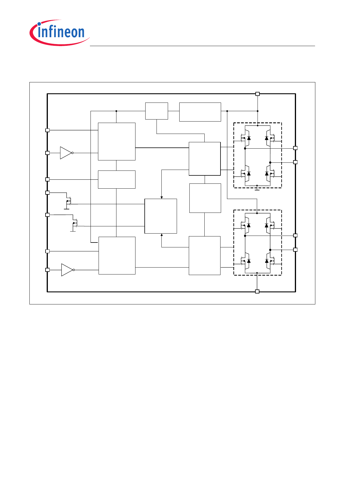
Block Diagram
Data Sheet
4
Rev. 1.1, 2009-07-07
2
Block Diagram
Figure 1
Block Diagram
Inhibit
INH
EF1
EF2
IN1
IN2
IN3
IN4
VS
OUT1
OUT2
OUT3
OUT4
GND
Protected
Driver
Stage
OUT1+2
Protected
Driver
Stage
OUT3+4
TLE8444
Vs monitor
under/overvoltage
detection
Function
Logic
OUT3+4
Function
Logic
OUT1+2
Charge
Pump
Internal
Supply
Error Flag
Generation
Data Sheet
5
Rev. 1.1, 2009-07-07
TLE 8444SL
Block Diagram
Figure 2
Terms
INH
EFx
INx
VS
OUTx
GND
TLE8444
V
S
V
INH,
V
INHH,
V
INHL
V
EFx,
V
EFLx
I
S
I
EFLKx
I
INx
I
INHH
I
OUTx
V
FU
V
DSHSx
V
DSLSx
V
FL
V
INx,
V
INHx,
V
INLx
I
GND
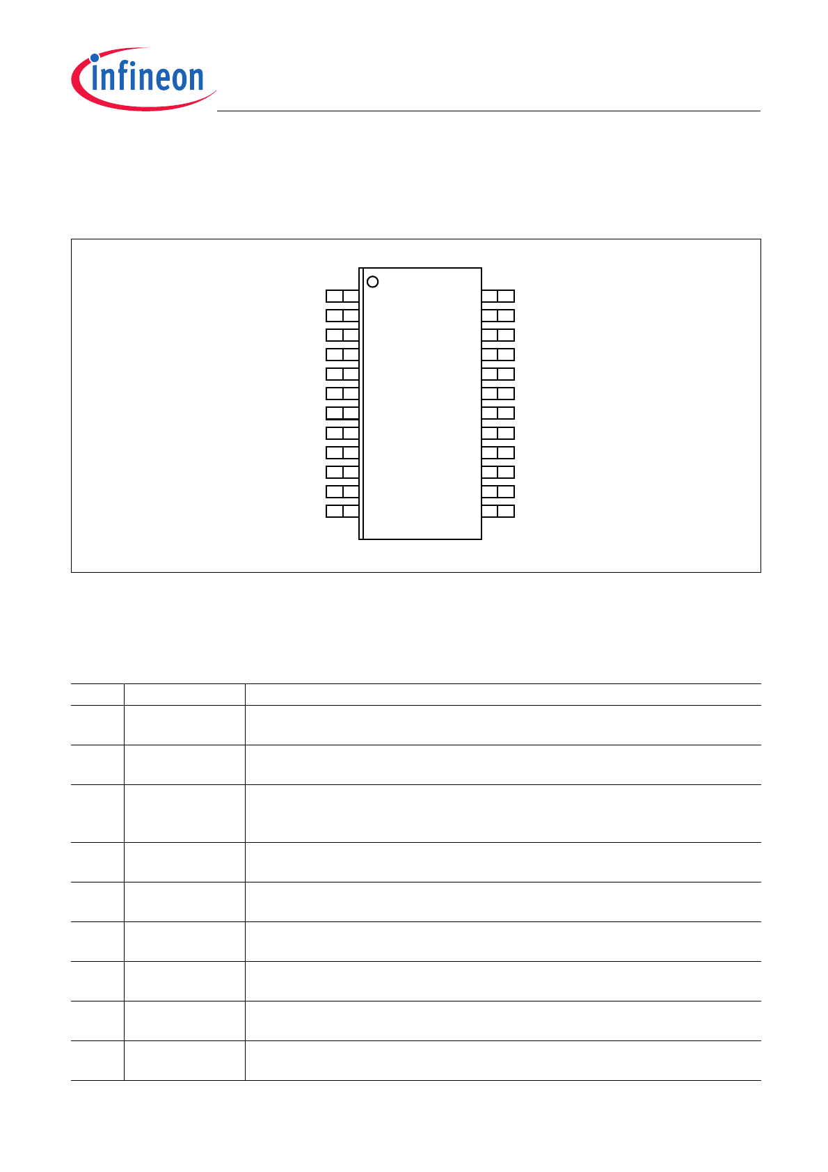
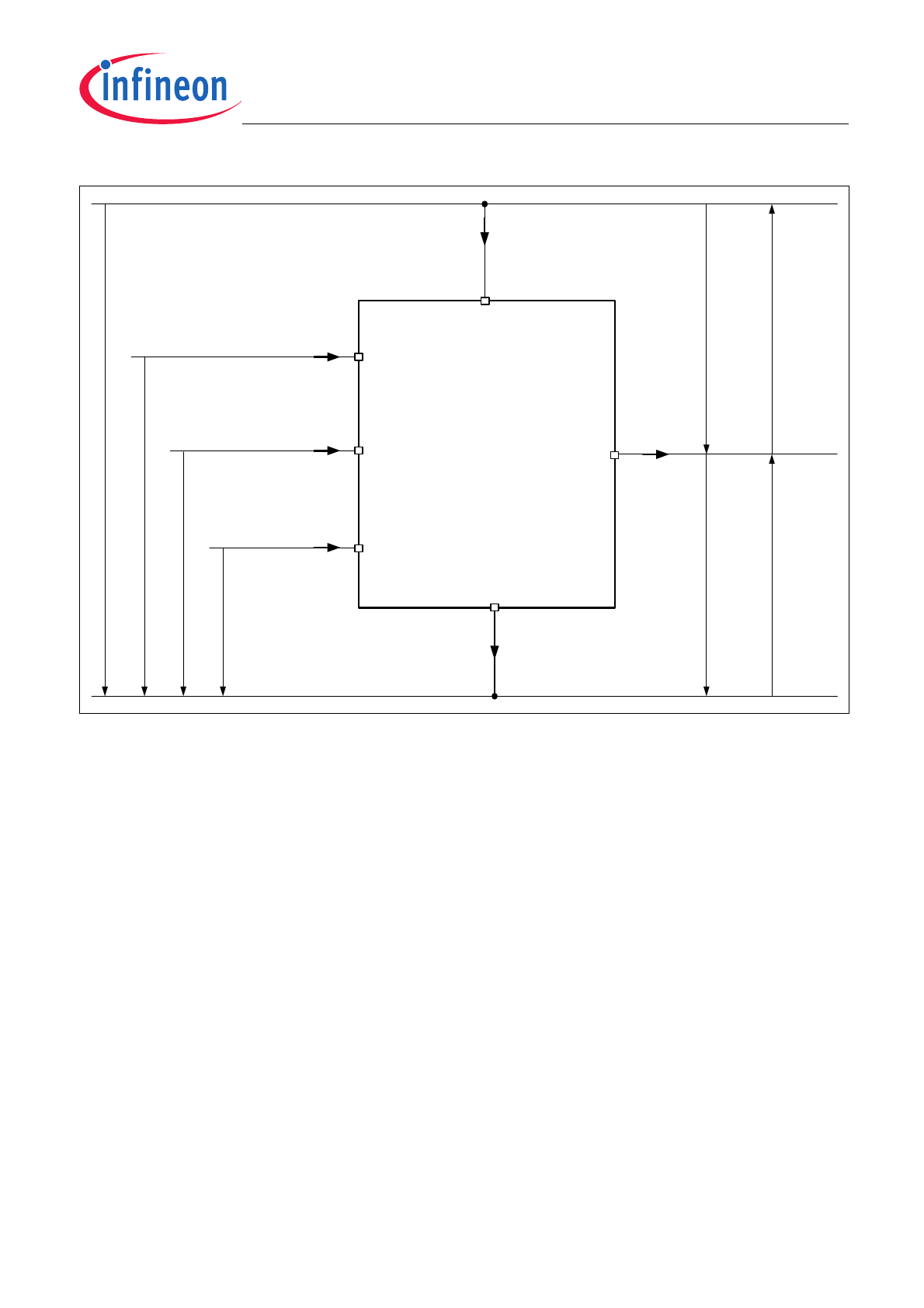
TLE 8444SL
Pin Configuration
Data Sheet
6
Rev. 1.1, 2009-07-07
3
Pin Configuration
3.1
Pin Assignment
Figure 3
Pin Configuration
3.2
Pin Definitions and Functions
Pin
Symbol
Function
1, 2, 11,
12, 20
GND
Ground; Signal ground; All GND pins must be externally connected together to the
common GND potential
3
OUT1
Power Output of Half-bridge 1
Short circuit protected; with integrated free-wheeling diodes
4, 9, 15,
22
V
S
Power Supply Voltage; All
V
S
pins must be externally connected together to the
Battery Voltage with Reverse protection Diode, buffer capacitance and Filter against
EMC. See Application Diagram,
Figure 18
and
Figure 19
for more information
5
EF1
Error Flag 1 (Diagnosis Output)
Open drain by default; Low = error
6
IN1
Input Channel of Half-bridge 1
Controls OUT1,
Non-inverting Intput with internal Pull Down
7
IN2
Input Channel of Half-bridge 2
Controls OUT2, Inverting Input with internal Pull Up
8
EF2
Error Flag 2 (Diagnosis Output)
Open drain by default; Low = error
10
OUT2
Power Output of Half-bridge 2
Short circuit protected; with integrated free-wheeling diodes
13, 16,
21, 24
N.C.
Not Connected
n.c.
OUT3
VS
n.c.
GND
IN3
IN4
IN2
EF2
VS
OUT 2
GND
GND
GND
GND
OUT 1
VS
EF1
IN1
INH
n.c.
VS
OUT 4
n.c.
18
17
16
15
14
13
24
23
22
21
20
19
1
2
3
4
5
6
7
8
9
10
11
12

Data Sheet
7
Rev. 1.1, 2009-07-07
TLE 8444SL
Pin Configuration
14
OUT4
Power Output of Half-bridge 4
Short circuit protected; with integrated free-wheeling diodes
17
INH
Inhibit Input
Low = Device in sleep mode
18
IN4
Input Channel of Half-bridge 4
Controls OUT4,
Inverting Input with internal Pull Up
19
IN3
Input Channel of Half-bridge 3
Controls OUT3,
Non-inverting Intput with internal Pull Down
23
OUT3
Power Output of Half-bridge 3
Short-circuit protected; with integrated free-wheeling diodes
Pin
Symbol
Function

TLE 8444SL
General Product Characteristics
Data Sheet
8
Rev. 1.1, 2009-07-07
4
General Product Characteristics
4.1
Absolute Maximum Ratings
Note: Stresses above the ones listed here may cause permanent damage to the device. Exposure to absolute
maximum rating conditions for extended periods may affect device reliability.
Note: Integrated protection functions are designed to prevent IC destruction under fault conditions described in the
data sheet. Fault conditions are considered as “outside” normal operating range. Protection functions are
not designed for continuous repetitive operation.
Absolute Maximum Ratings
1)
T
j
= -40
°
C to +150
°
C; all voltages with respect to ground, positive current flowing into pin (unless otherwise
specified)
1) Not subject to production test, specified by design.
Pos.
Parameter
Symbol
Limit Values
Unit
Conditions
Min.
Max.
Voltages
4.1.1
Supply voltage
V
S
-0.3
40
V
–
4.1.2
Logic input voltages
(IN1; IN2; IN3; IN4; INH)
V
IN(1-4)
V
INH
-0.3
5.5
V
0 V <
V
S
< 40 V
4.1.3
Logic output voltage
(EF
1
; EF
2
)
V
EF(1+2)
-0.3
5.5
V
0 V <
V
S
< 40 V
Currents
4.1.4
Output current (diode)
I
OUT(1-4)
-1
1
A
–
4.1.5
Output current (EF
1
; EF
2
)
I
EF(1-2)
-2
5
mA
–
Temperatures
4.1.6
Junction temperature
T
j
-40
150
°
C
–
4.1.7
Storage temperature
T
stg
-50
150
°
C
–
ESD Susceptibility
4.1.8
ESD capability of OUT and
V
S
pin vers.
GND
V
ESD
-2
2
kV
2)
2) Human Body Model according to ANSI EOS\ESD S5.1 standard (eqv. to MIL STD 883D and JEDEC JESD22-A114)
4.1.9
ESD capability of logic pins vers. GND
V
ESD
-2
2
kV
2)
Data Sheet
9
Rev. 1.1, 2009-07-07
TLE 8444SL
General Product Characteristics
4.2
Functional Range
Note: Within the functional range the IC operates as described in the circuit description. The electrical
characteristics are specified within the conditions given in the related electrical characteristics table.
4.3
Thermal Resistance
Note: This thermal data was generated in accordance with JEDEC JESD51 standards. For more information, go
to
www.jedec.org
.
Pos.
Parameter
Symbol
Limit Values
Unit
Conditions
Min.
Max.
4.2.1
Supply Voltage Range for
Normal Operation
V
S(nor)
8
18
V
–
4.2.2
Extended Supply Voltage Range
for Operation
V
S(ext)
V
UV OFF
V
OV OFF
V
Limit values,
deviations possible;
After
V
S
rising above
V
UV ON
4.2.3
Supply voltage increasing
V
S
-0.3
V
UV ON
V
Outputs are open
4.2.4
Supply voltage decreasing
V
S
-0.3
V
UV OFF
V
Outputs are open
4.2.5
Logic input voltages
(IN1; IN2; IN3; IN4; INH)
V
IN(1-4)
V
INH
-0.3
5.5
V
–
4.2.6
Junction temperature
T
j
-40
150
°
C
–
Pos.
Parameter
Symbol
Limit Values
Unit
Conditions
Min.
Typ.
Max.
4.3.1
Junction to Soldering Point
1)
1) Not subject to production test, specified by design
R
thJSP
–
–
26
K/W
pin 1, 2, 11, 12
2)
2) Specified RthJS value is simulated at natural convection on a cold plate setup (all pins are fixed to ambient temperature).
Ta=25°C, LS1+HS2+LS3+HS4 are dissipating 1W (0.25W each).
4.3.2
Junction to Ambient
1)
R
thJA
–
60
–
K/W
3)
3) Specified RthJA value is according to Jedec JESD51-2,-7 at natural convection on FR4 2s2p board; The Product
(Chip+Package) was simulated on a 76.2 x 114.3 x 1.5 mm board with 2 inner copper layers (2 x 70µm Cu, 2 x 35µm Cu).
Ta=25°C, LS1+HS2+LS3+HS4 are dissipating 1W (0.25W each).

TLE 8444SL
General Product Characteristics
Data Sheet
10
Rev. 1.1, 2009-07-07
4.4
Electrical Characteristics
4.4.3
Electrical Characteristics
V
S
= 8 V to 18 V,
T
j
= -40
°
C to +150
°
C, INH = HIGH;
I
OUT1-4
= 0 A; all voltages with respect to ground, positive
current flowing into pin (unless otherwise specified)
Pos.
Parameter
Symbol
Limit Values
Unit Conditions
Min.
Typ.
Max.
Current Consumption, INH = GND
4.4.1
Quiescent current
I
S
–
1
5
µ
A
V
S
= 13.5 V;
T
j
< 85
°
C
Current Consumption, INH = HIGH
4.4.2
Supply current
I
S
–
5
10
mA
IN1+3=L, IN2+4=H
Over- and Under Voltage Lockout
4.4.3
UV Switch ON voltage
V
UV ON
4.2
–
5
V
V
S
increasing, see
Figure 6
4.4.4
UV Switch OFF voltage
V
UV OFF
4
–
4.8
V
V
S
decreasing, see
Figure 6
4.4.5
UV ON/OFF hysteresis
V
UV HY
0.05
0.26
0.7
V
V
UV ON
-
V
UV OFF,
see
Figure 7
4.4.6
OV Switch OFF voltage
V
OV OFF
21
–
25
V
V
S
increasing, see
Figure 6
4.4.7
OV Switch ON voltage
V
OV ON
20
–
24
V
V
S
decreasing, see
Figure 6
4.4.8
OV ON/OFF hysteresis
V
OV HY
–
1
–
V
V
OV OFF
-
V
OV ON,
see
Figure 7
Static Drain-source ON-Resistance
4.4.9
High- and low-side switch
R
DSON
–
0.6
0.8
Ω
I
OUT
= ±0.8 A; T
j
= 25 °C
–
1.0
1.3
Ω
I
OUT
= ±0.8 A; T
j
= 150 °C
Output Protection and Diagnosis
4.4.10
Short Circuit Current
1)
I
SC(1-4)
1.8
2.4
3.2
A
HS+LS each Channel, see
Figure 13
4.4.11
Overcurrent Shutdown
Threshold
I
SD(1-4)
0.9
1.2
1.6
A
4.4.12
Shutdown Delay Time
t
dSD(1-4)
10
25
50
µs
4.4.13
Open Load Detection
Current
I
OLD(1-4)
6
12
20
mA
each LS Channel
, see
Figure 15
4.4.14
Open Load Delay Time
t
dOLD(1-4)
200
350
600
µs
Output Switching Times
4.4.15
high-side ON delay-time
t
dONH
7
10
14
µs
V
S
=13.5V, resistive Load
=100
Ω
,
see
Figure 16
and
Figure 17
4.4.16
high-side switch ON time
t
ONH
2
6
9
µs
4.4.17
high-side OFFdelay-time
t
dOFFH
1
2
4
µs
4.4.18
high-side switch OFF time
t
OFFH
0.2
1
2
µs
4.4.19
low-side ON delay-time
t
dONL
2
5
8
µs
4.4.20
low-side switch ON time
t
ONL
0.5
1
3
µs
4.4.21
low-side OFF delay-time
t
dOFFL
1
2
5
µs
4.4.22
low-side switch OFF time
t
OFFL
0.5
1
2
µs
4.4.23
dead-time
t
DB
0.1
2
–
µs
t
dONH
- t
ONH
- t
dOFFL
or
t
dONL
- t
ONL
- t
dOFFH
Outputs OUT(1-4), Freewheeling Diodes
4.4.24
Forward voltage; upper
V
FU
–
1
1.5
V
I
F
= 0.4 A, INH = LOW