

N e v e r s t o p t h i n k i n g .
I S O F A C E
T M
I S O 1 H 8 0 1 G
C o r e l e s s T r a n s f o r m e r I s o l a t e d
D i g i t a l O u t p u t 8 C h a n n e l 0 . 6 2 5 A
H i g h - S i d e S w i t c h
D a t a s h e e t , V e r s i o n 2 . 3 , S e p t e m b e r 2 0 0 9
P o w e r M a n a g e m e n t & D r i v e s

ISO1H801G
Revision History:
2009-09-16
Version 2.3
Previous Version:
V2.2
V2.0
Final Datasheet
V2.1
Final Datasheet
V2.2
Page 15 creepage, clearance distance and V
ISO
adapted,
V2.3
Diagnostic output discontinued
Edition 2009-09-16
Published by Infineon Technologies AG,
Am Campeon 1-12,
85579 Neubiberg, Germany
©
Infineon Technologies AG 2009.
All Rights Reserved.
Attention please!
The information herein is given to describe certain components and shall not be considered as a guarantee of
characteristics.
Terms of delivery and rights to technical change reserved.
We hereby disclaim any and all warranties, including but not limited to warranties of non-infringement, regarding
circuits, descriptions and charts stated herein.
Information
For further information on technology, delivery terms and conditions and prices please contact your nearest
Infineon Technologies Office (
www.infineon.com
).
Warnings
Due to technical requirements components may contain dangerous substances. For information on the types in
question please contact your nearest Infineon Technologies Office.
Infineon Technologies Components may only be used in life-support devices or systems with the express written
approval of Infineon Technologies, if a failure of such components can reasonably be expected to cause the failure
of that life-support device or system, or to affect the safety or effectiveness of that device or system. Life support
devices or systems are intended to be implanted in the human body, or to support and/or maintain and sustain
and/or protect human life. If they fail, it is reasonable to assume that the health of the user or other persons may
be endangered.
Type
On-state Resistance
Package
ISO1H801G
200m
Ω
PG-DSO-36
Datasheet
3
Version 2.3, 2009-09-16
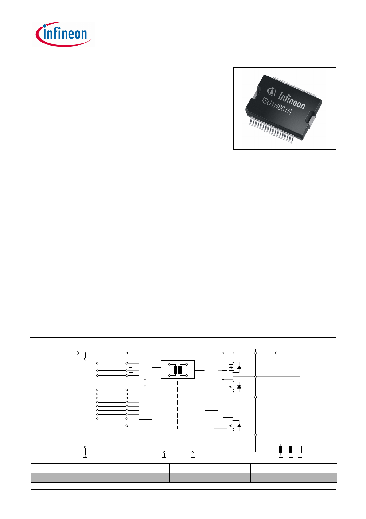
ISOFACE
TM
ISO1H801G
Coreless Transformer Isolated Digital
Output 8 Channel 0.625A High-Side Switch
Product Highlights
•
Coreless transformer isolated data interface
•
Galvanic isolation
•
8 High-side output switches 0.625A
•
µC compatible 8-bit parallel peripheral
ISO1H801G
µC (i.e
C166)
AD0
WR
P0.0
P0.1
P0.2
P0.3
P0.4
P0.5
P0.6
P0.7
P1.x
VCC
VCC
Parallel
Interface
Control
Unit
CT
Control
&
Protectio
n Unit
CS
WR
D0
D1
D2
D3
D4
D5
D6
D7
DIS
VCC
GNDCC
GNDbb
GND
OUT7
Vbb
Vbb
OUT1
OUT0
Typical Application
reserved
Features
•
Interface 5V CMOS operation compatible
•
Parallel interface
•
Direct control mode
•
High common mode transient immunity
•
Short circuit protection
•
Maximum current internally limited
•
Overload protection
•
Overvoltage protection (including load dump)
•
Undervoltage shutdown with autorestart and
hysteresis
•
Switching inductive loads
•
Common output disable pin
•
Thermal shutdown with restart
•
Thermal independence of separate channels
•
ESD protection
•
Loss of GNDbb and loss of V
bb
protection
•
Reverse Output Voltage protection
Typical Application
•
Isolated switch for industrial applications (PLC)
•
All types of resistive, inductive and capacitive loads
•
µC compatible power switch for 24V DC
applications
•
Driver for solenoid, relays and resistive loads
Description
The ISO1H801G is a galvanically isolated 8 bit data
interface in PG-DSO-36 package that provides 8 fully
protected high-side power switches that are able to
handle currents up to 625 mA.
An 8 bit parallel µC compatible interface allows to
connect the IC directly to a µC system. The input
interface supports also a direct control mode and is
designed to operate with 5V CMOS compatible levels.
The data transfer from input to output side is realized by
the integrated Coreless Transformer Technology.
ISOFACE™
ISO1H801G
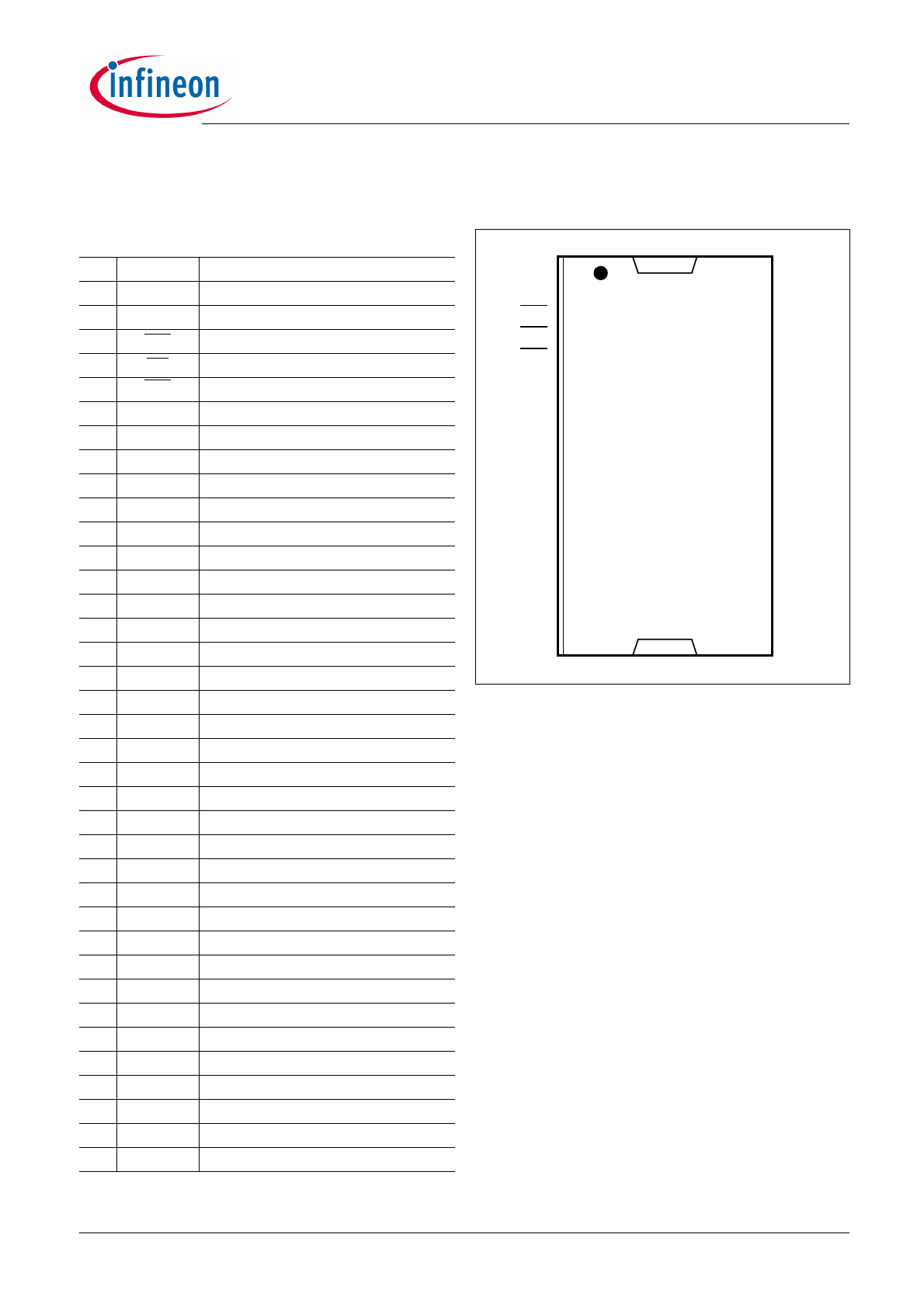
Pin Configuration and Functionality
Datasheet
4
Version 2.3, 2009-09-16
1
Pin Configuration and Functionality
1.1
Pin Configuration
Pin
Symbol
Function
1
N.C.
Not connected
2
VCC
Positive 5V logic supply
3
DIS
Output disable
4
CS
Chip select
5
WR
Parallel write
6
D0
Data input bit0
7
D1
Data input bit1
8
D2
Data input bit2
9
D3
Data input bit3
10
D4
Data input bit4
11
D5
Data input bit5
12
D6
Data input bit6
13
D7
Data input bit7
14
reserved
-
15
GNDCC
Input logic ground
16
N.C.
Not connected
17
N.C.
Not connected
18
N.C.
Not connected
19
GNDbb
Output driver ground
20
N.C
Not connected
21
OUT7
High-side output of channel 7
22
OUT7
High-side output of channel 7
23
OUT6
High-side output of channel 6
24
OUT6
High-side output of channel 6
25
OUT5
High-side output of channel 5
26
OUT5
High-side output of channel 5
27
OUT4
High-side output of channel 4
28
OUT4
High-side output of channel 4
29
OUT3
High-side output of channel 3
30
OUT3
High-side output of channel 3
31
OUT2
High-side output of channel 2
32
OUT2
High-side output of channel 2
33
OUT1
High-side output of channel 1
34
OUT1
High-side output of channel 1
35
OUT0
High-side output of channel 0
36
OUT0
High-side output of channel 0
TAB
Vbb
Positive driver power supply voltage
VCC
D1
1
DIS
CS
WR
5
4
2
3
D3
D5
D2
D4
D0
6
7
8
9
10
D6
11
D7
12
reserved
13
GNDCC
14
15
N.C.
16
17
18
36
32
33
35
34
31
30
29
28
27
26
25
24
23
22
21
20
19
OUT0
OUT2
OUT0
OUT1
OUT1
OUT3
OUT4
OUT3
OUT4
OUT2
OUT5
OUT5
OUT6
OUT6
GNDbb
OUT7
OUT7
N.C.
N.C.
N.C.
N.C.
Vbb
Vbb
TAB
TAB
Figure 1
Power SO-36 (430mil)
.

Datasheet
5
Version 2.3, 2009-09-16
ISOFACE™
ISO1H801G
Pin Configuration and Functionality
1.2
Pin Functionality
VCC (Positive 5V logic supply)
The VCC supplies the input interface that is
galvanically isolated from the output driver stage. The
input interface can be supplied with 5V.
DIS (Output disable)
The high-side outputs OUT0...OUT7 can be
immediately switched off by means of the low active pin
DIS that is an asynchronous signal. The input registers
are also reset by the
DIS signal. The Output remains
switched off after low-high transition of DIS signal, till
new information is written into the input register.
Current Sink to GNDCC.
CS (Chip select)
The system microcontroller selects the ISO1H801G by
means of the low active pin
CS to activate the parallel
interface. By connecting the
CS pin and WR pin to
ground the parallel direct control is activated. Current
Source to VCC.
WR (Parallel write)
In parallel mode data at the input pins (D0 ... D7) are
latched by means of the rising edge of the low active
signal
WR (write). Current Source to VCC.
D0 ... D7 (Data input bit0 ... bit7)
The present data can be latched on the rising edge of
the write signal
WR. D0 ... D7 control the corresponding
output channels OUT0 ...OUT7. By connecting CS and
WR to ground, the signals at D0 ... D7 directly control
the outputs. Current Sink to GNDCC.
GNDCC (Ground for VCC domain)
This pin acts as the ground reference for the input
interface that is supplied by VCC.
GNDbb (Output driver ground domain)
This pin acts as the ground reference for the output
driver that is supplied by Vbb.
OUT0 ... OUT7 (High side output channel 0 ... 7)
The output high side channels are internally connected
to Vbb and controlled by the corresponding data input
pins D0 ... D7 in parallel mode.
TAB (Vbb, Positive supply for output driver)
The heatslug is connected to the positive supply port of
the output interface.
Datasheet
6
Version 2.3, 2009-09-16
ISOFACE™
ISO1H801G
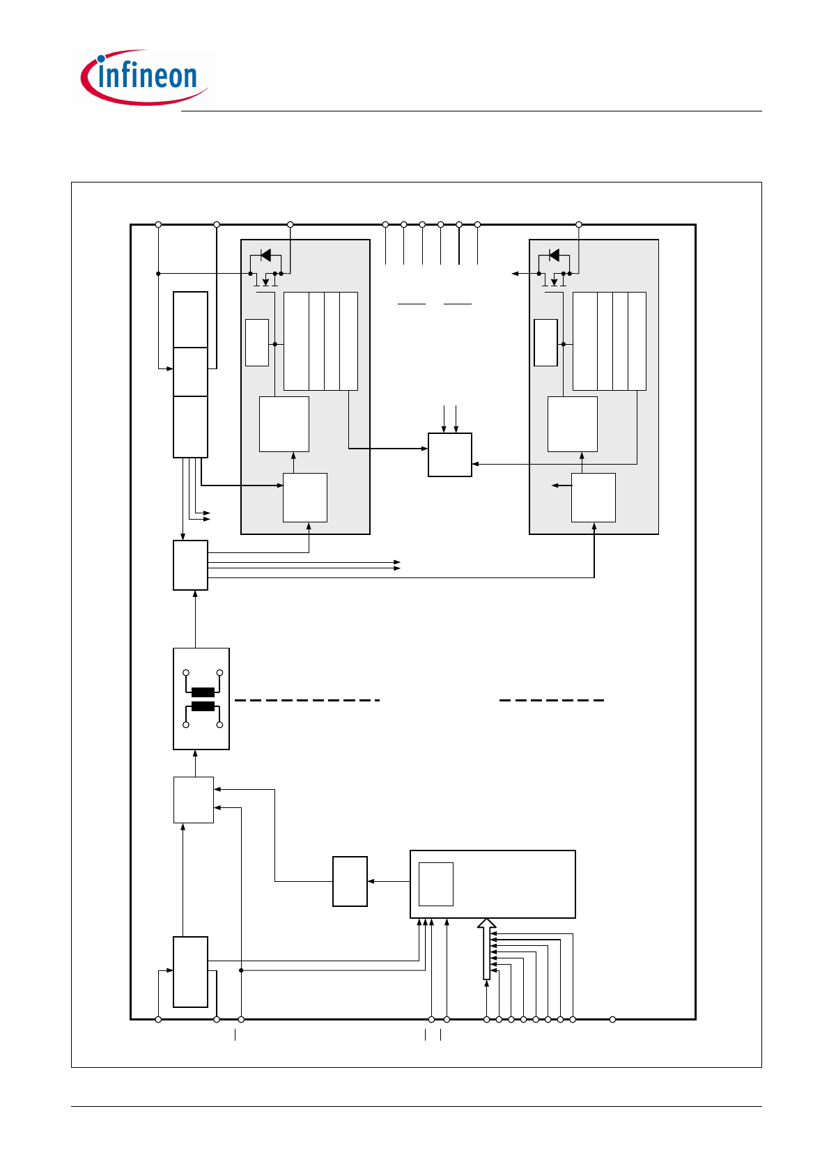
Blockdiagram
2
Blockdiagram
Pa
ra
lle
l
In
pu
t I
nte
rf
ac
e
< D
0 -
D
7
>
D1
D2
D3
D4
D5
D6
D7
D0
WR
CS
O
ver
vo
ltag
e
P
rot
ec
tion
U
nde
rv
ol
tage
S
hut
dow
n w
ith
Re
st
ar
t
V
ol
ta
ge
So
ur
ce
C
om
m
on
D
iagn
os
tic
Ou
tp
ut
Se
ria
l
to
Pa
ra
lle
l
to
Lo
gi
c
C
han
nel
1 -
6
Temper
at
ur
e S
ens
or
OU
T0
O
ve
rload
P
ro
tec
tion
C
ur
rent
Li
m
ita
tion
Li
m
ita
tio
n of
U
nc
lamped
Indu
ct
iv
e Loa
d
Logi
c
C
har
ge
Pu
m
p
Le
ve
l s
hi
fter
Re
ct
ifi
er
Hi
gh
-s
id
e Ch
an
n
el
0
Temper
at
ur
e S
ens
or
OU
T7
O
ve
rload
P
ro
tec
tion
C
ur
rent
Li
m
ita
tion
Li
m
ita
tio
n of
U
nc
lamped
Indu
ct
iv
e Loa
d
Logi
c
C
har
ge
Pu
m
p
Le
ve
l S
hi
fte
r
Re
ct
ifi
er
Hi
gh
-s
id
e Ch
an
n
el
7
C
han
ne
l 1
...
6
fr
o
m
Tem
per
at
ur
e S
en
so
r
C
h
an
n
el
1 -
6
to
Lo
gi
c
C
ha
nne
l 1
-
6
Vb
b
Logi
c
U
nde
rv
ol
tage
S
hut
dow
n w
ith
Re
st
ar
t
Vb
b
G
NDb
b
VC
C
GN
D
C
C
Gal
vanic
Isol
atio
n
DI
S
OU
T1
OU
T2
OU
T3
OU
T4
OU
T5
OU
T6
Ga
te
P
rot
ec
tion
Ga
te
P
rot
ec
tion
IS
O
1H
801
G
Di
re
ct
Mode
Co
nt
ro
l
re
se
rv
ed
Pa
ra
lle
l
to
Se
ria
l
CT
Figure 2
Blockdiagram
ISOFACE™
ISO1H801G
Functional Description
Datasheet
7
Version 2.3, 2009-09-16
3
Functional Description
3.1
Introduction
The ISOFACE ISO1H801G includes 8 high-side power
switches that are controlled by means of the integrated
parallel interface. The interface is 8bit µC compatible.
Furthermore a direct control mode can be selected that
allows the direct control of the outputs OUT0...OUT7 by
means of the inputs D0...D7 without any additional logic
signal. The IC can replace 8 optocouplers and the 8
high-side switches in conventional I/O-Applications as
a galvanic isolation is implemented by means of the
integrated coreless transformer technology. The µC
compatible interfaces allow a direct connection to the
ports of a microcontroller without the need for other
components. Each of the 8 high-side power switches is
protected against short to Vbb, overload,
overtemperature and against overvoltage by an active
zener clamp.
The diagnostic logic on the power chip recognizes the
overtemperature information of each power transistor.
3.2
Power Supply
The IC contains 2 galvanic isolated voltage domains
that are independent from each other. The input
interface is supplied at VCC and the output stage is
supplied at Vbb. The different voltage domains can be
switched on at different time. The output stage is only
enabled once the input stage enters a stable state.
3.3
Output Stage
Each channel contains a high-side vertical power FET
that is protected by embedded protection functions.
The continous current for each channel is 625mA (all
channels ON).
3.3.1
Output Stage Control
Each output is independently controlled by an output
latch and a common reset line via the pin
DIS that
disables all eight outputs and reset the latches. The
parallel input data is transferred to the input latches
with a high-to-low transition of the signal
WR (write)
while the
CS is logic low. A low-to-high transition of CS
transfers then the data of the input latches to the output
buffer.
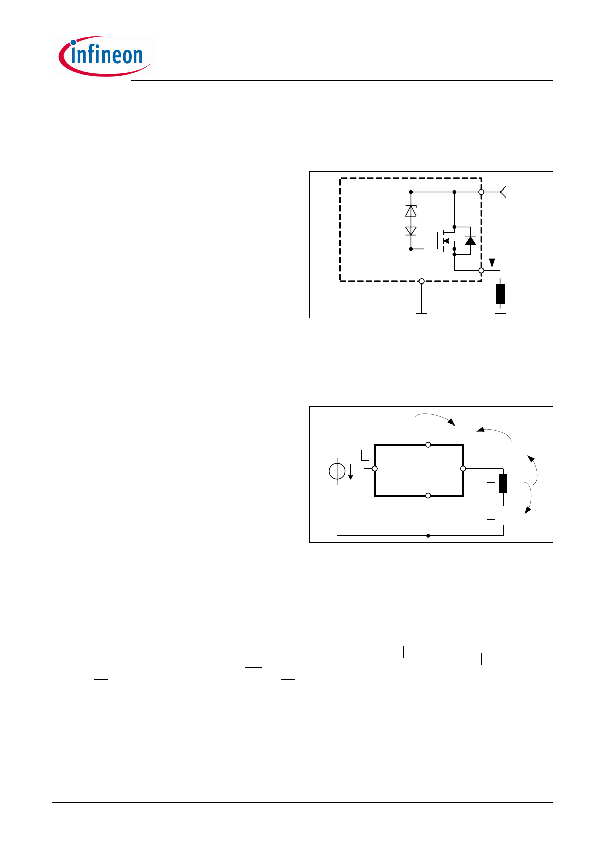
3.3.2
Power Transistor Overvoltage
Protection
Each of the eight output stages has it own zener clamp
that causes a voltage limitation at the power transistor
when solenoid loads are switched off. V
ON
is then
clamped to 47V (min.).
Vz
Vbb
GNDbb
OUTx
V
ON
Vbb
Figure 3
Inductive and overvoltage output
clamp (each channel)
Energy is stored in the load inductance during an
inductive load switch-off.
E
L
1 2
⁄
L I
L
2
×
×
=
E
L
GNDbb
V
bb
OUTx
E
R
L
R
L
E
Load
Z
L
Vbb
E
bb
E
AS
Dx
Figure 4
Inductive load switch-off energy
dissipation (each channel)
While demagnetizing the load inductance, the energy
dissipation in the DMOS is
E
AS
E
bb
E
L
E
R
–
V
ON CL
(
)
i
L
t
( )dt
×
=
+
=
with an approximate solution for R
L
> 0
Ω:
E
AS
I
L
L
×
2 R
L
×
----------------
V
bb
V
ON CL
(
)
+
(
)
1
I
L
R
L
×
V
ON CL
(
)
-------------------------
+
ln
×
×
=
3.3.3
Power Transistor Overcurrent
Protection
The outputs are provided with a current limitation that
enters a repetitive switched mode after an initial peak
current has been exceeded. The initial peak short
circuit current limit is set to I
L(SCp)
. During the repetitive
mode short circuit current the limit is set to I
L(SCr)
. If this
operation leads to an overtemperature condition, a
second protection level (T
j
> 135°C) will change the
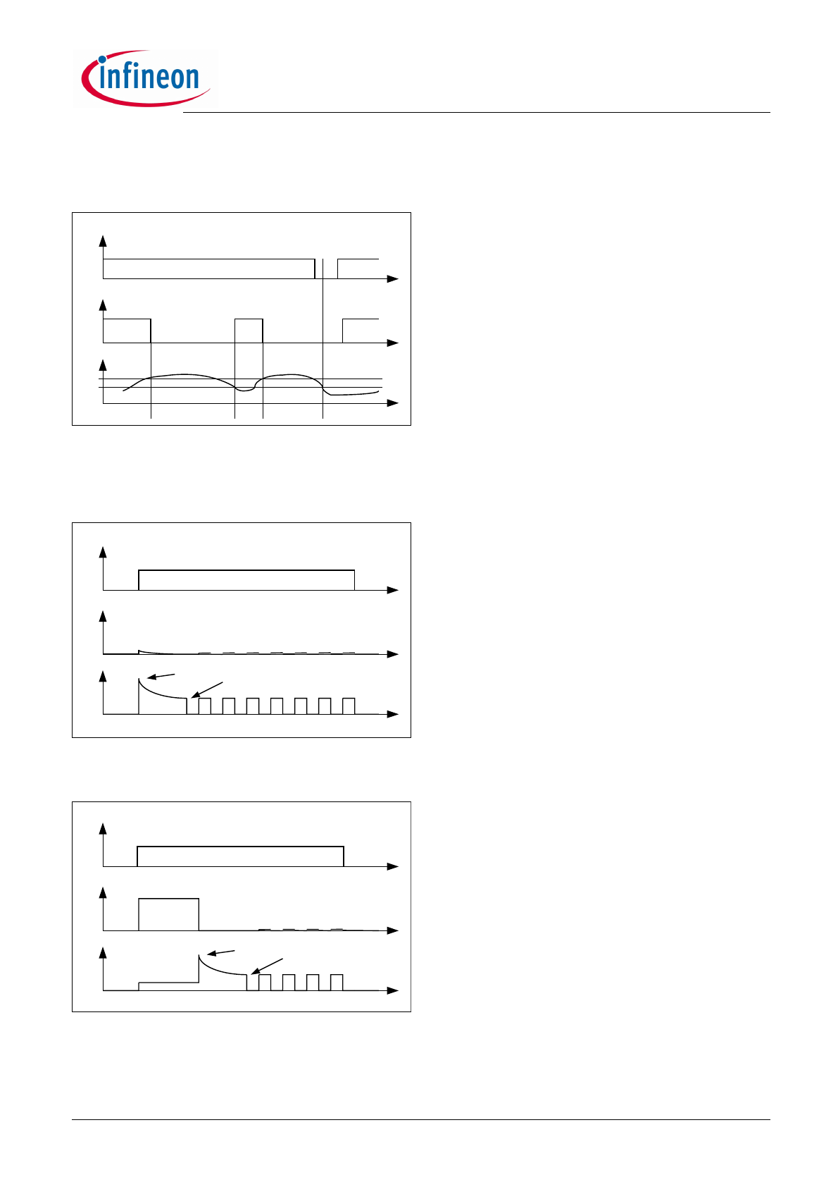
Datasheet
8
Version 2.3, 2009-09-16
ISOFACE™
ISO1H801G
Functional Description
output into a low duty cycle PWM (selective thermal
shutdown with restart) to prevent critical chip
temperatures.
IN
VOUT
T
J
t
t
t
Figure 5
Overtemperature detection
The following figures show the timing for a turn on into
short circuit and a short circuit in on-state. Heating up
of the chip may require several milliseconds,
depending on external conditions.
IN
VOUT
I
L
t
t
t
Output short to GND
I
L(SCp)
I
L(SCr)
Figure 6
Turn on into short circuit, shut down by
overtemperature, restart by cooling
IN
VOUT
I
L
t
t
t
Output short to GND
I
L(SCp)
I
L(SCr)
Normal
operation
Figure 7
Short circuit in on-state, shut down
down by overtemperature, restart by
cooling
3.4
Reserved
Datasheet
9
Version 2.3, 2009-09-16
ISOFACE™
ISO1H801G
Functional Description
3.5
Parallel Interface
The ISO1H801G contains a parallel interface that can
be directly controlled by the microcontroller output
ports. The parallel interface can also be switched over
to a direct control that allows direct changes of the
outputs OUT0 ... OUT7 by means of the corresponding
inputs D0 ... D7 without additional logic signals. To
activate the parallel direct control mode pin
CS and pin
WR have to be connected both to GNDCC.
3.5.1
Parallel Interface Signal
Description
CS - Chip select. The system microcontroller selects
the ISO1H801G by means of the
CS pin. Whenever the
pin is in a logic low state, data can be transferred from
the µC.
CS High to low transition:
•
Parallel input data can be written in from then on
CS Low to high transition:
•
The data in the input latches is transferred to the
output buffer
WR - Write. The system controller enables the write
procedure in the ISO1H801G by means of the signal
WR. A logic low state signal at pin WR writes the input
data into the input latches when the
CS pin is in a logic
low state.
WR Logic low level:
•
Parallel input data at the pins D0 - D7 is written into
the input latches
WR Logic high level:
•
The parallel input data is latched in the input
latches. Any changes at the pins D0 - D7 after the
low-to-high transition of
WR do not affect the input
latches.
D0 ... D7 - Parallel input. Parallel data bits are fed into
the pins D0 ... D7. The data is written into the input
latches when
WR is logic low.
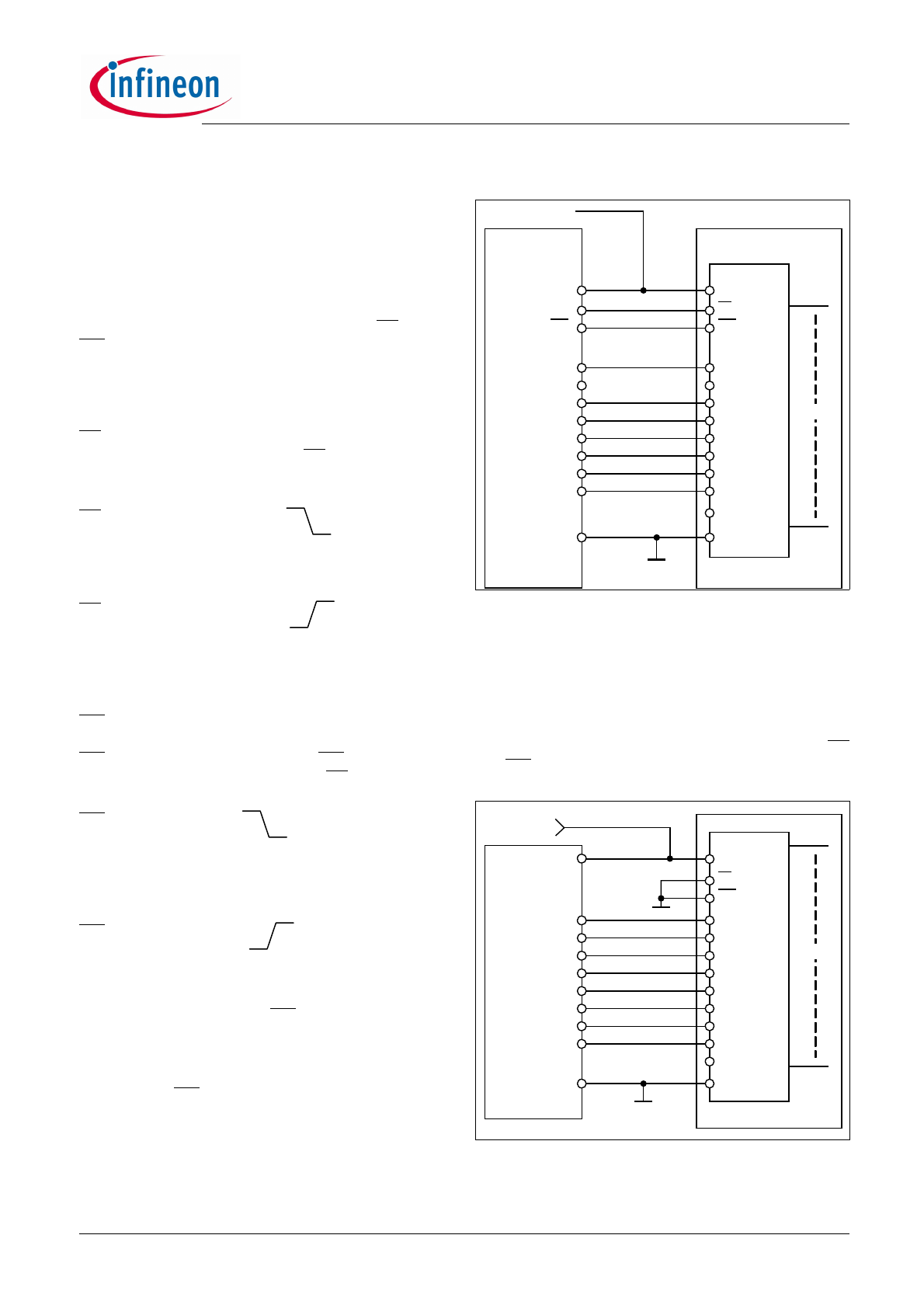
3.5.2
uC Control Mode
P
ar
al
lel
Inter
fac
e
IC1
Output
lines
µC (i.e
C166)
CS
WR
AD0
WR
P0
P1
P2
P3
P4
P5
P6
P7
D0
D1
D2
D3
D4
D5
D6
D7
reserved
VCC
VCC
VCC
GNDCC
GND
Figure 8
Parallel bus configuration
3.5.3
Direct Control Mode
Beside the use of the parallel µC compatible interface a
parallel direct control mode can be choosen. In this
mode the output OUT0...OUT7 can be directly
controlled via the inputs D0...D7 without the need for
additional logic signals. To activate this mode pin
CS
and
WR need to be connected to GNDCC.
.
P
ar
al
le
l In
te
rfa
ce
IC1
Output
lines
Controller
P0
P1
P2
P3
P4
P5
P6
P7
D0
D1
D2
D3
D4
D5
D6
D7
VCC
VCC
VCC
CS
WR
reserved
GNDCC
GND
Figure 9
Parallel Direct Control
Datasheet
10
Version 2.3, 2009-09-16
ISOFACE™
ISO1H801G
Functional Description
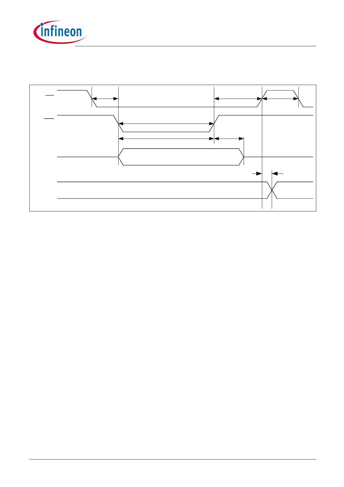
3.6
Parallel Interface Timing
CS
WR
DATA
t
WHCS
t
WRPW
D0 - D7
t
DS
t
DH
t
CSWR
t
CSD
OUT0 - OUT7
t
on/off
OUTPUT
Figure 10
Parallel input - output timing diagram
3.7
Transmission Failure Detection
There is a failure detection unit integrated to ensure also a stable functionality during the integrated coreless
transformer transmission. This unit decides wether the transmitted data is valid or not. If four times serial data
coming in from the internal registers is not accepted, the output stages are switched off until the next valid data is
received.