

2 E D 0 2 0 I 1 2 - F I
D u a l I G B T D r i v e r I C
P o w e r M a n a g m e n t & D r i v e s
F i n a l D a t a s h e e t , S e p t e m b e r 2 0 0 7
N e v e r s t o p t h i n k i n g .

Edition 2007-09-10
Published by Infineon Technologies AG,
Am Campeon 1-12,
D-85579 Neubiberg
©
Infineon 2007.
All Rights Reserved.
Attention please!
The information herein is given to describe certain components and shall not be considered as warranted char-
acteristics.
Terms of delivery and rights to technical change reserved.
We hereby disclaim any and all warranties, including but not limited to warranties of non-infringement, regarding
circuits, descriptions and charts stated herein.
Infineon Technologies AG is an approved CECC manufacturer.
Information
For further information on technology, delivery terms and conditions and prices, please contact your nearest Infi-
neon office in Germany or our Infineon representatives worldwide (see at http://www.infineon.com).
Warnings
Due to technical requirements components may contain dangerous substances. For information on the types in
question, please contact your nearest Infineon office.
Infineon components may only be used in life-support devices or systems with the express written approval of In-
fineon, if a failure of such components can reasonably be expected to cause the failure of that life-support device
or system, or to affect the safety or effectiveness of that device or system. Life support devices or systems are
intended to be implanted in the human body, or to support and/or maintain and sustain and/or protect human life.
If they fail, it is reasonable to assume that the health of the user or other persons may be endangered.
For questions on technology, delivery and prices, please contact the Infineon offices in Germany or the Infineon
companies and representatives worldwide:
See our webpage at http://www.infineon.com/gatedriver
2ED020I12-FI
Revision History: 2007-09-10 Final Datasheet
Previous Version:
Preliminary Datasheet V3.2 2ED020I12-FI
Page
Subjects (major changes since last revision)
12
Update Operating Range
21
Update Application Advices
Type
Ordering Code
Package
Packaging
2ED020I12-FI
SP0002-65782
PG-DSO-18-2 Tape&Reel
2ED020I12-FI
Final Data
Final Datasheet
3
September 2007
PG-DS O-18-2
Dual IGBT Driver IC
2ED020I12-FI
Product Highlights
• Fully operational to ±1.2 kV
• Power supply operating range from 14 to 18 V
• Gate drive currents of +1 A / –2 A
• Matched propagation delay for both channels
• High dV/dt immunity
• Low power consumption
• General purpose operational amplifier
• General purpose comparator
Features
• Floating high side driver
• Undervoltage lockout for both channels
• 3.3 V and 5 V TTL compatible inputs
• CMOS Schmitt-triggered inputs with pull-down
• Non-inverting inputs
• Interlocking inputs
• Dedicated shutdown input with pull-up
• RoHS compliant

High and Low Side Driver
2ED020I12-FI
Overview
Final Datasheet
4
September 2007
Final Data
1
Overview
The 2ED020I12-FI is a high voltage, high speed power MOSFET and IGBT driver with
interlocking high and low side referenced outputs. The floating high side driver may be
supplied directly or by means of a bootstrap diode and capacitor. In addition to the logic
input of each driver the 2ED020I12-FI is equipped with a dedicated shutdown input. All
logic inputs are compatible with 3.3 V and 5 V TTL. The output drivers feature a high
pulse current buffer stage designed for minimum driver cross-conduction. Propagation
delays are matched to simplify use in high frequency applications. Both drivers are
designed to drive an N-channel power MOSFET or IGBT which operate up to 1.2 kV. In
addition, a general purpose operational amplifier and a general purpose comparator are
provided which may be used for instance for current measurement or overcurrent
detection.
High and Low Side Driver
2ED020I12-FI
Pin Configuration and Functionality
Final Datasheet
5
September 2007
Final Data
2
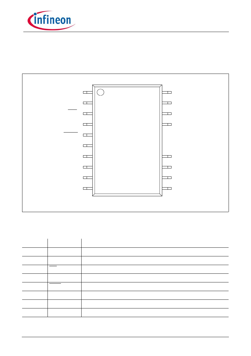
Pin Configuration and Functionality
2.1
Pin Configuration
VSH
GNDH
OP+
OutL
VSL
P-DSO-18-2 (300mil)
n.c.
OP -
OPO
CP+
2E
D
020I
12-
FI
GND
OutH
InL
CPO
InH
GNDH
CP -
SD
GNDL
Figure 1 Pin Configuration (top view)
2.2
Pin Definitions and Functions
Pin
Symbol
Function
1
InH
Logic input for high side driver
2
InL
Logic input for low side driver
3
SD
Logic input for shutdown of both drivers
4
GND
Common ground
5
CPO
Open collector output of general purpose comparator
6
CP–
Inverting input of general purpose comparator
7
CP+
Non-inverting input of general purpose comparator
8
OPO
Output of general purpose OP
Table 1
Pin Description
High and Low Side Driver
2ED020I12-FI
Pin Configuration and Functionality
Final Datasheet
6
September 2007
Final Data
9
OP–
Inverting input of general purpose OP
10
OP+
Non-inverting input of general purpose OP
11
GNDL
Low side power ground
1)
12
OutL
Low side gate driver output
13
VSL
Low side supply voltage
14
n.c.
(not connected)
15
n.e.
(not existing)
16
n.e.
(not existing)
17
GNDH
High side (power) ground
18
VSH
High side supply voltage
19
OutH
High side gate driver output
20
GNDH
High side (power) ground
1)
Please note : GNDL has to be connected directly to GND
Pin
Symbol
Function
Table 1
Pin Description (cont’d)
High and Low Side Driver
2ED020I12-FI
Block Diagram
Final Datasheet
7
September 2007
Final Data
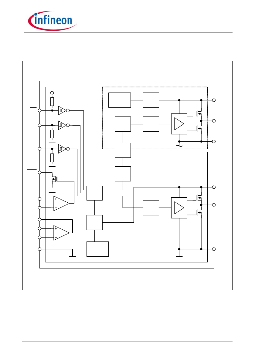
3
Block Diagram
SD
CPO
InH
Input
Logic
Delay
TX
RX
Logic
UVLO
Voltage
Supply
High Side
UVLO
Voltage
Supply
OP
OPO
OP+
OP -
Low Side
CP+
CLT
CP
CP -
InL
V
CC
GND
VSH
OutH
GNDH
OutL
GNDL
VSL
Figure 2 Block Diagram

High and Low Side Driver
2ED020I12-FI
Functional Description
Final Datasheet
8
September 2007
Final Data
4
Functional Description
4.1
Power Supply
The power supply of both sides, “VSL” and “VSH”, is monitored by an undervoltage
lockout block (UVLO) which enables operation of the corresponding side when the
supply voltage reaches the “on” threshold. Afterwards the internal voltage reference and
the biasing circuit are enabled. When the supply voltage (VSL, VSH) drops below the
“off” threshold, the circuit is disabled.
4.2
Logic Inputs
The logic inputs InH, InL and SD are fed into Schmitt-Triggers with thresholds compatible
to 3.3V and 5V TTL. When SD is enabled (low), InH and InL are disabled. If InH is high
(while InL is low), OutH is enabled and vice versa. However, if both signals are high, they
are internally disabled until one of them gets low again. This is due to the interlocking
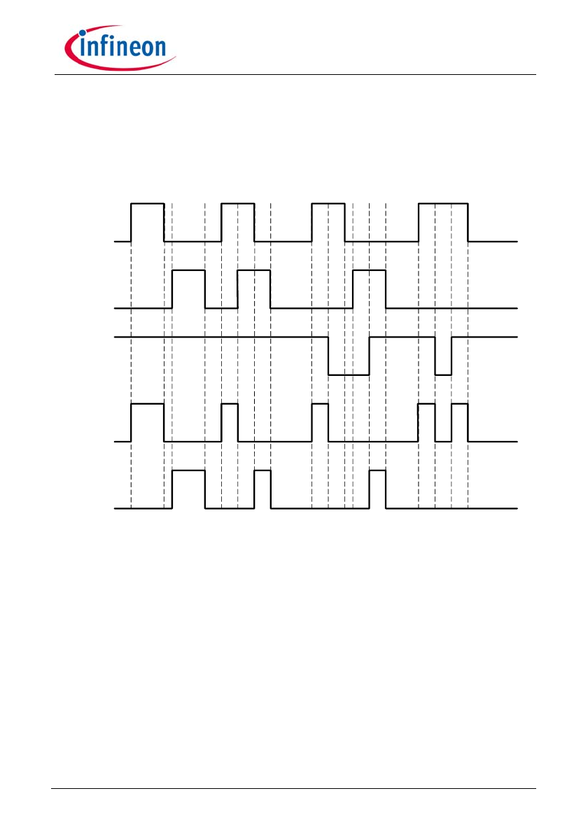
logic of the device. See Figure 3 (section 4.7).
4.3
Gate Driver
2ED020I12-FI features two hard-switching gate drivers with N-channel output stages
capable to source 1A and to sink 2A peak current. Both drivers are equipped with active-
low-clamping capability. Furthermore, they feature a large ground bounce ruggedness
in order to compensate ground bounces caused by a turn-off of the driven IGBT.
4.4
General Purpose Operational Amplifier
This general purpose operational amplifier can be applied for current measurement of
the driven low-side IGBT. It is dedicated for fast operation with a gain of at least 3. The
OP is equipped with a -0.1 to 2V input stage and a rail-to-rail output stage which is
capable to drive
±
5mA.
4.5
General Purpose Comparator
The general purpose comparator can be applied for overcurrent detection of the low side
IGBT. A dedicated offset as well as a pull-up and pull-down resistor has been introduced
to its inputs for security reasons.
4.6
Coreless Transformer (CLT)
In order to enable signal transmission across the isolation barrier between low-side and
high-side driver, a transformer based on CLT-Technology is employed. Signals, that are
to be transmitted, are specially encoded by the transmitter and correspondingly restored
by the receiver. In this way EMI due to variations of GNDH (dV
GNDH
/dt) or the magnetic
flux density (d
Η
/dt) can be suppresed.To compensate the additional propagation delay
High and Low Side Driver
2ED020I12-FI
Functional Description
Final Datasheet
9
September 2007
Final Data
of transmitter, level shifter and receiver, a dedicated propagation delay is introduced into
the low-side driver.
4.7
Diagrams
InH
InL
/SD
OutH
OutL
Figure 3 Input/Output Timing Diagram
High and Low Side Driver
2ED020I12-FI
Electrical Parameters
Final Datasheet
10
September 2007
Final Data
5
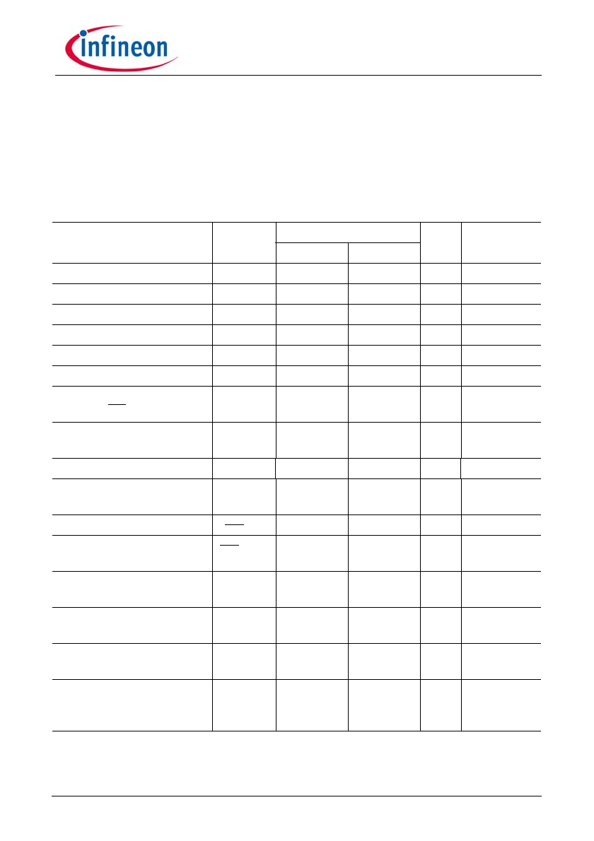
Electrical Parameters
5.1
Absolute Maximum Ratings
Note: Absolute maximum ratings are defined as ratings, which when being exceeded
may lead to destruction of the integrated circuit. Unless otherwise noted all
parameters refer to GND.
Parameter
Symbol
Limit Values
Unit
Remarks
min.
max.
High side ground
GNDH
– 1200
1200
V
High side supply voltage
VSH
– 0.3
20
V
1)
High side gate driver output OutH
– 0.3
VSH + 0.3
V
1)
Low side ground
GNDL
– 0.3
5.3
V
Low side supply voltage
VSL
– 0.3
20
V
2)
Low side gate driver output
OutL
– 0.3
VSL + 0.3
V
3)
Logic input voltages
(InH, InL, SD)
V
IN
– 0.3
5.3
V
OP input voltages
(OP–, OP+)
V
OP
– 0.3
5.3
V
4)
OP output voltage
V
OPO
– 0.3
5.3
V
CP input voltages
(CP–, CP+)
V
CP
– 0.3
5.3
V
4)
CP output voltage
V
CPO
– 0.3
5.3
V
CP output maximal sink
current
I
CPO
—
5
mA
High side ground, voltage
transient
dV
GNDH
/dt – 50
50
V/ns
ESD Capability
V
ESD
—
2
kV
5)
Human
Body Model
Package power disipation
@T
A
= 25°C
P
D
—
1.4
W
6)
Thermal resistance (both
chips active), junction to
ambient
R
THJA
—
90
K/W
7)