
1
TechnischeInformation/TechnicalInformation
F5-75R06KE3_B5
IGBT-Module
IGBT-modules
preparedby:CM
approvedby:RS
dateofpublication:2013-11-04
revision:2.2
ULapproved(E83335)
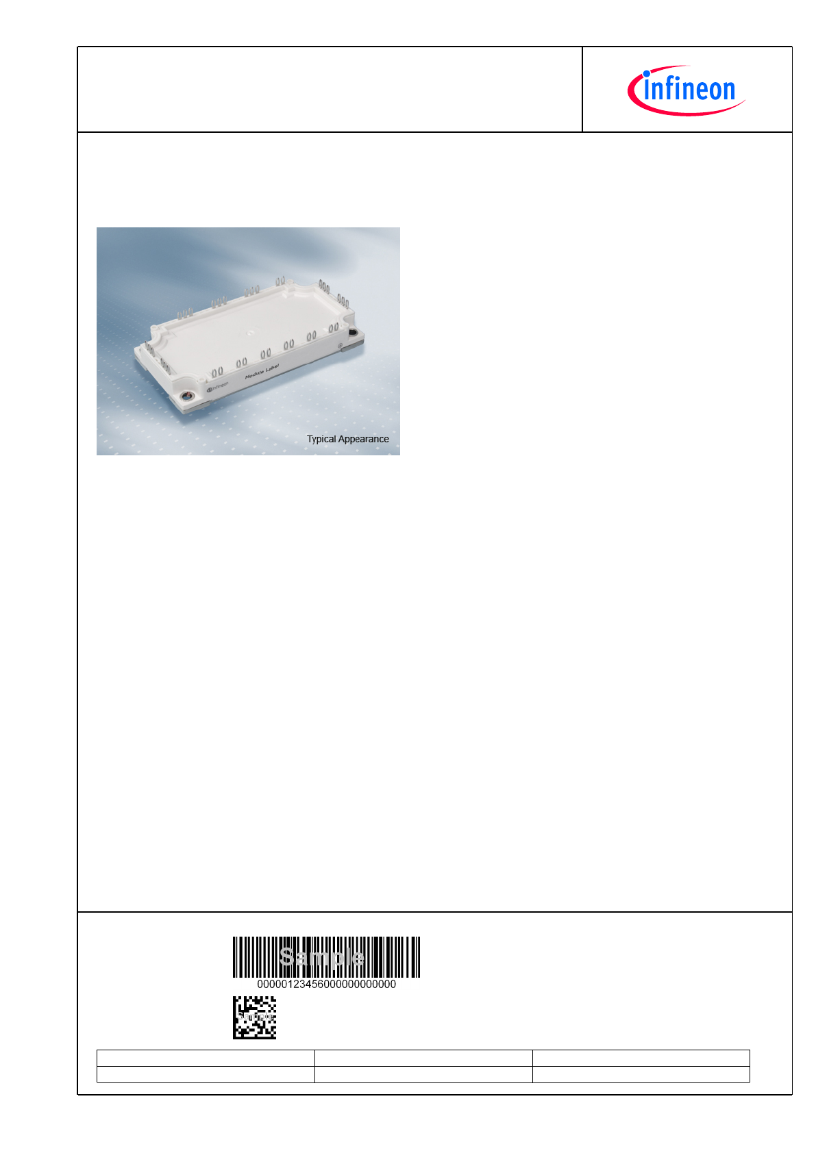
EconoPACK™3ModulmitTrench/FeldstoppIGBT3undEmitterControlled3DiodeundPressFIT/NTC
EconoPACK™3modulewithTrench/FieldstopIGBT3andEmitterControlled3diodeandPressFIT/NTC
VorläufigeDaten/PreliminaryData
V
CES
= 600V
I
C nom
= 75A / I
CRM
= 150A
TypischeAnwendungen
TypicalApplications
•
•
SolarAnwendungen
SolarApplications
ElektrischeEigenschaften
ElectricalFeatures
•
•
TrenchIGBT3
TrenchIGBT3
•
•
NiedrigesV
CEsat
LowV
CEsat
MechanischeEigenschaften
MechanicalFeatures
•
•
IntegrierterNTCTemperaturSensor
IntegratedNTCtemperaturesensor
•
•
Kupferbodenplatte
CopperBasePlate
•
•
PressFITVerbindungstechnik
PressFITContactTechnology
ModuleLabelCode
BarcodeCode128
DMX-Code
ContentoftheCode
Digit
ModuleSerialNumber
1-5
ModuleMaterialNumber
6-11
ProductionOrderNumber
12-19
Datecode(ProductionYear)
20-21
Datecode(ProductionWeek)
22-23

2
TechnischeInformation/TechnicalInformation
F5-75R06KE3_B5
IGBT-Module
IGBT-modules
preparedby:CM
approvedby:RS
dateofpublication:2013-11-04
revision:2.2
VorläufigeDaten
PreliminaryData
IGBT,Wechselrichter/IGBT,Inverter
HöchstzulässigeWerte/MaximumRatedValues
Kollektor-Emitter-Sperrspannung
Collector-emittervoltage
T
vj
= 25°C
V
CES
600
V
Kollektor-Dauergleichstrom
ContinuousDCcollectorcurrent
T
C
= 80°C, T
vj max
= 175°C
I
C nom
75
A
PeriodischerKollektor-Spitzenstrom
Repetitivepeakcollectorcurrent
t
P
= 1 ms
I
CRM
150
A
Gesamt-Verlustleistung
Totalpowerdissipation
T
C
= 25°C, T
vj max
= 175°C
P
tot
250
W
Gate-Emitter-Spitzenspannung
Gate-emitterpeakvoltage
V
GES
+/-20
V
CharakteristischeWerte/CharacteristicValues
min.
typ.
max.
Kollektor-Emitter-Sättigungsspannung
Collector-emittersaturationvoltage
I
C
= 75 A, V
GE
= 15 V
I
C
= 75 A, V
GE
= 15 V
I
C
= 75 A, V
GE
= 15 V
V
CE sat
1,45
1,60
1,70
1,90
V
V
V
T
vj
= 25°C
T
vj
= 125°C
T
vj
= 150°C
Gate-Schwellenspannung
Gatethresholdvoltage
I
C
= 1,20 mA, V
CE
= V
GE
, T
vj
= 25°C
V
GEth
4,9
5,8
6,5
V
Gateladung
Gatecharge
V
GE
= -15 V ... +15 V
Q
G
0,80
µC
InternerGatewiderstand
Internalgateresistor
T
vj
= 25°C
R
Gint
0,0
Ω
Eingangskapazität
Inputcapacitance
f = 1 MHz, T
vj
= 25°C, V
CE
= 25 V, V
GE
= 0 V
C
ies
4,60
nF
Rückwirkungskapazität
Reversetransfercapacitance
f = 1 MHz, T
vj
= 25°C, V
CE
= 25 V, V
GE
= 0 V
C
res
0,145
nF
Kollektor-Emitter-Reststrom
Collector-emittercut-offcurrent
V
CE
= 600 V, V
GE
= 0 V, T
vj
= 25°C
I
CES
1,0
mA
Gate-Emitter-Reststrom
Gate-emitterleakagecurrent
V
CE
= 0 V, V
GE
= 20 V, T
vj
= 25°C
I
GES
100
nA
Einschaltverzögerungszeit,induktiveLast
Turn-ondelaytime,inductiveload
I
C
= 75 A, V
CE
= 300 V
V
GE
= ±15 V
R
Gon
= 5,1
Ω
t
d on
0,025
0,025
0,025
µs
µs
µs
T
vj
= 25°C
T
vj
= 125°C
T
vj
= 150°C
Anstiegszeit,induktiveLast
Risetime,inductiveload
I
C
= 75 A, V
CE
= 300 V
V
GE
= ±15 V
R
Gon
= 5,1
Ω
t
r
0,02
0,02
0,02
µs
µs
µs
T
vj
= 25°C
T
vj
= 125°C
T
vj
= 150°C
Abschaltverzögerungszeit,induktiveLast
Turn-offdelaytime,inductiveload
I
C
= 75 A, V
CE
= 300 V
V
GE
= ±15 V
R
Goff
= 5,1
Ω
t
d off
0,21
0,24
0,25
µs
µs
µs
T
vj
= 25°C
T
vj
= 125°C
T
vj
= 150°C
Fallzeit,induktiveLast
Falltime,inductiveload
I
C
= 75 A, V
CE
= 300 V
V
GE
= ±15 V
R
Goff
= 5,1
Ω
t
f
0,06
0,07
0,07
µs
µs
µs
T
vj
= 25°C
T
vj
= 125°C
T
vj
= 150°C
EinschaltverlustenergieproPuls
Turn-onenergylossperpulse
I
C
= 75 A, V
CE
= 300 V, L
S
= 30 nH
V
GE
= ±15 V, di/dt = 4000 A/µs (T
vj
= 150°C)
R
Gon
= 5,1
Ω
E
on
0,35
0,50
0,60
mJ
mJ
mJ
T
vj
= 25°C
T
vj
= 125°C
T
vj
= 150°C
AbschaltverlustenergieproPuls
Turn-offenergylossperpulse
I
C
= 75 A, V
CE
= 300 V, L
S
= 30 nH
V
GE
= ±15 V, du/dt = 4000 V/µs (T
vj
= 150°C)
R
Goff
= 5,1
Ω
E
off
2,40
2,80
3,00
mJ
mJ
mJ
T
vj
= 25°C
T
vj
= 125°C
T
vj
= 150°C
Kurzschlußverhalten
SCdata
V
GE
≤
15 V, V
CC
= 360 V
V
CEmax
= V
CES
-L
sCE
·di/dt
I
SC
530
380
A
A
T
vj
= 25°C
T
vj
= 150°C
t
P
≤
8 µs,
t
P
≤
6 µs,
Wärmewiderstand,ChipbisGehäuse
Thermalresistance,junctiontocase
proIGBT/perIGBT
R
thJC
0,60
K/W
Wärmewiderstand,GehäusebisKühlkörper
Thermalresistance,casetoheatsink
proIGBT/perIGBT
λ
Paste
=1W/(m·K)/
λ
grease
=1W/(m·K)
R
thCH
0,21
K/W
TemperaturimSchaltbetrieb
Temperatureunderswitchingconditions
T
vj op
-40
150
°C

3
TechnischeInformation/TechnicalInformation
F5-75R06KE3_B5
IGBT-Module
IGBT-modules
preparedby:CM
approvedby:RS
dateofpublication:2013-11-04
revision:2.2
VorläufigeDaten
PreliminaryData
Diode,Wechselrichter/Diode,Inverter
HöchstzulässigeWerte/MaximumRatedValues
PeriodischeSpitzensperrspannung
Repetitivepeakreversevoltage
T
vj
= 25°C
V
RRM
600
V
Dauergleichstrom
ContinuousDCforwardcurrent
I
F
75
A
PeriodischerSpitzenstrom
Repetitivepeakforwardcurrent
t
P
= 1 ms
I
FRM
150
A
Grenzlastintegral
I²t-value
V
R
= 0 V, t
P
= 10 ms, T
vj
= 125°C
V
R
= 0 V, t
P
= 10 ms, T
vj
= 150°C
I²t
660
610
A²s
A²s
CharakteristischeWerte/CharacteristicValues
min.
typ.
max.
Durchlassspannung
Forwardvoltage
I
F
= 75 A, V
GE
= 0 V
I
F
= 75 A, V
GE
= 0 V
I
F
= 75 A, V
GE
= 0 V
V
F
1,55
1,50
1,45
1,95
V
V
V
T
vj
= 25°C
T
vj
= 125°C
T
vj
= 150°C
Rückstromspitze
Peakreverserecoverycurrent
I
F
= 75 A, - di
F
/dt = 4000 A/µs (T
vj
=150°C)
V
R
= 300 V
V
GE
= -15 V
I
RM
100
115
125
A
A
A
T
vj
= 25°C
T
vj
= 125°C
T
vj
= 150°C
Sperrverzögerungsladung
Recoveredcharge
I
F
= 75 A, - di
F
/dt = 4000 A/µs (T
vj
=150°C)
V
R
= 300 V
V
GE
= -15 V
Q
r
3,00
6,00
7,50
µC
µC
µC
T
vj
= 25°C
T
vj
= 125°C
T
vj
= 150°C
AbschaltenergieproPuls
Reverserecoveryenergy
I
F
= 75 A, - di
F
/dt = 4000 A/µs (T
vj
=150°C)
V
R
= 300 V
V
GE
= -15 V
E
rec
0,95
1,50
1,85
mJ
mJ
mJ
T
vj
= 25°C
T
vj
= 125°C
T
vj
= 150°C
Wärmewiderstand,ChipbisGehäuse
Thermalresistance,junctiontocase
proDiode/perdiode
R
thJC
0,95
K/W
Wärmewiderstand,GehäusebisKühlkörper
Thermalresistance,casetoheatsink
proDiode/perdiode
λ
Paste
=1W/(m·K)/
λ
grease
=1W/(m·K)
R
thCH
0,33
K/W
TemperaturimSchaltbetrieb
Temperatureunderswitchingconditions
T
vj op
-40
150
°C

4
TechnischeInformation/TechnicalInformation
F5-75R06KE3_B5
IGBT-Module
IGBT-modules
preparedby:CM
approvedby:RS
dateofpublication:2013-11-04
revision:2.2
VorläufigeDaten
PreliminaryData
MOSFET/MOSFET
HöchstzulässigeWerte/MaximumRatedValues
Drain-Source-Sperrspannung
Drain-sourcebreakdownvoltage
T
vj
= 25°C
V
DSS
600
V
Drain-Gleichstrom
DCdraincurrent
T
C
= 80°C
T
C
= 25°C
I
D nom
I
D
70
80
A
A
GepulsterDrainstrom,tplimitiertdurch
Tjmax
Pulseddraincurrent,tplimitedbyTjmax
I
D puls
210
A
Gesamt-Verlustleistung
Totalpowerdissipation
T
C
= 25°C
P
tot
1200
W
Gate-Source-Spitzenspannung
Gate-sourcepeakvoltage
V
GSS
+/-20
V
CharakteristischeWerte/CharacteristicValues
min.
typ.
max.
Einschaltwiderstand
Drain-sourceonresistance
I
D
= 70 A, V
GS
= 10 V, T
vj
= 25°C
R
DS on
22,0
m
Ω
Gate-Schwellenspannung
Gatethresholdvoltage
I
D
= 9,00 mA, V
DS
= V
GS
, T
vj
= 25°C
V
GS(th)
3,00
4,00
5,00
V
Gateladung
Gatecharge
V
GS
= 10 V, V
DD
= 480 V
Q
G
0,25
µC
InternerGatewiderstand
Internalgateresistor
T
vj
= 25°C
R
Gint
1,3
Ω
Eingangskapazität
Inputcapacitance
f = 1 MHz, T
vj
= 25°C, V
DS
= 25 V, V
GS
= 0 V
C
iss
23,0
nF
Ausgangskapazität
Outputcapacitance
f = 1 MHz, T
vj
= 25°C, V
DS
= 25 V, V
GS
= 0 V
C
oss
6,60
nF
Rückwirkungskapazität
Reversetransfercapacitance
f = 1 MHz, T
vj
= 25°C, V
DS
= 25 V, V
GS
= 0 V
C
rss
0,23
nF
Drain-Source-Reststrom
Zerogatevoltagedraincurrent
V
DS
= 600 V, V
GS
= 0 V, T
vj
= 25°C
I
DSS
100
µA
Gate-Source-Reststrom
Gate-sourceleakagecurrent
V
DS
= 0 V, V
GS
= 20 V, T
vj
= 25°C
I
GSS
0,10
nA
Einschaltverzögerungszeit,induktiveLast
Turnondelaytime,inductiveload
I
D
= 70 A, V
DS
= 400 V
V
GS
= 10 V
R
G
= 10,0
Ω
t
d on
0,18
0,17
ns
T
vj
= 25°C
T
vj
= 125°C
Anstiegszeit,induktiveLast
Risetime,inductiveload
I
D
= 70 A, V
DS
= 400 V
V
GS
= 10 V
R
G
= 10,0
Ω
t
r
0,075
0,075
ns
T
vj
= 25°C
T
vj
= 125°C
Abschaltverzögerungszeit,induktiveLast
Turnoffdelaytime,inductiveload
I
D
= 70 A, V
DS
= 400 V
V
GS
= 10 V
R
G
= 10,0
Ω
t
d off
0,50
0,53
ns
T
vj
= 25°C
T
vj
= 125°C
Fallzeit,induktiveLast
Falltime,inductiveload
I
D
= 70 A, V
DS
= 400 V
V
GS
= 10 V
R
G
= 10,0
Ω
t
f
0,03
0,035
ns
T
vj
= 25°C
T
vj
= 125°C
EinschaltverlustenergieproPuls
Turn-onenergylossperpulse
I
D
= 70 A, V
DS
= 400 V, L
σ
= 30 nH
V
GS
= 10 V
R
G
= 10,0
Ω
E
on
1,90
mJ
T
vj
= 25°C
T
vj
= 125°C
AbschaltverlustenergieproPuls
Turn-offenergylossperpulse
I
D
= 70 A, V
DS
= 400 V, L
σ
= 30 nH
V
GS
= 10 V
R
G
= 10,0
Ω
E
off
1,05
mJ
T
vj
= 25°C
T
vj
= 125°C
Wärmewiderstand,ChipbisGehäuse
Thermalresistance,junctiontocase
R
thJC
0,12
K/W
Wärmewiderstand,GehäusebisKühlkörper
Thermalresistance,casetoheatsink
pro MOS-FET / per MOS-FET
λ
Paste
= 1 W/(m*K) /
λ
grease
= 1 W/(m*K)
R
thCH
0,042
K/W
TemperaturimSchaltbetrieb
Temperatureunderswitchingconditions
T
vj op
-40
125
°C
Revers-Diode/reverse-diode
min.
typ.
max.
Durchlassspannung
Forwardvoltage
I
S
= 70 A, V
GS
= 0 V
I
S
= 70 A, V
GS
= 0 V
V
SD
0,80
0,70
1,10
V
T
vj
= 25°C
T
vj
= 125°C

5
TechnischeInformation/TechnicalInformation
F5-75R06KE3_B5
IGBT-Module
IGBT-modules
preparedby:CM
approvedby:RS
dateofpublication:2013-11-04
revision:2.2
VorläufigeDaten
PreliminaryData
MOSFETOVP-Zweig/MOSFETOVP-Path
HöchstzulässigeWerte/MaximumRatedValues
Drain-Source-Sperrspannung
Drain-sourcebreakdownvoltage
T
vj
= 25°C
V
DSS
600
V
Drain-Gleichstrom
DCdraincurrent
T
C
= 80°C
T
C
= 25°C
I
D nom
I
D
70
80
A
A
GepulsterDrainstrom,tplimitiertdurch
Tjmax
Pulseddraincurrent,tplimitedbyTjmax
I
D puls
210
A
Gesamt-Verlustleistung
Totalpowerdissipation
T
C
= 25°C
P
tot
1200
W
Gate-Source-Spitzenspannung
Gate-sourcepeakvoltage
V
GSS
+/-20
V
CharakteristischeWerte/CharacteristicValues
min.
typ.
max.
Einschaltwiderstand
Drain-sourceonresistance
I
D
= 70 A, V
GS
= 10 V, T
vj
= 25°C
R
DS on
12,5
m
Ω
Gate-Schwellenspannung
Gatethresholdvoltage
I
D
= 9,00 mA, V
DS
= V
GS
, T
vj
= 25°C
V
GS(th)
2,50
3,00
3,50
V
Gateladung
Gatecharge
V
GS
= 10 V, V
DD
= 400 V
Q
G
0,45
µC
InternerGatewiderstand
Internalgateresistor
T
vj
= 25°C
R
Gint
1,3
Ω
Eingangskapazität
Inputcapacitance
f = 1 MHz, T
vj
= 25°C, V
DS
= 25 V, V
GS
= 0 V
C
iss
21,0
nF
Ausgangskapazität
Outputcapacitance
f = 1 MHz, T
vj
= 25°C, V
DS
= 25 V, V
GS
= 0 V
C
oss
45,0
nF
Rückwirkungskapazität
Reversetransfercapacitance
f = 1 MHz, T
vj
= 25°C, V
DS
= 25 V, V
GS
= 0 V
C
rss
0,90
nF
Drain-Source-Reststrom
Zerogatevoltagedraincurrent
V
DS
= 600 V, V
GS
= 0 V, T
vj
= 25°C
I
DSS
100
µA
Gate-Source-Reststrom
Gate-sourceleakagecurrent
V
DS
= 0 V, V
GS
= 20 V, T
vj
= 25°C
I
GSS
0,10
nA
Einschaltverzögerungszeit,induktiveLast
Turnondelaytime,inductiveload
I
D
= 70 A, V
DS
= 400 V
R
G
= 10,0
Ω
t
d on
0,03
0,035
ns
T
vj
= 25°C
T
vj
= 125°C
Anstiegszeit,induktiveLast
Risetime,inductiveload
I
D
= 70 A, V
DS
= 400 V
R
G
= 10,0
Ω
t
r
0,02
0,02
ns
T
vj
= 25°C
T
vj
= 125°C
Abschaltverzögerungszeit,induktiveLast
Turnoffdelaytime,inductiveload
I
D
= 70 A, V
DS
= 400 V
R
G
= 10,0
Ω
t
d off
0,10
0,11
ns
T
vj
= 25°C
T
vj
= 125°C
Fallzeit,induktiveLast
Falltime,inductiveload
I
D
= 70 A, V
DS
= 400 V
R
G
= 10,0
Ω
t
f
0,01
0,015
ns
T
vj
= 25°C
T
vj
= 125°C
EinschaltverlustenergieproPuls
Turn-onenergylossperpulse
I
D
= 70 A, V
DS
= 400 V, L
σ
= 30 nH
R
G
= 10,0
Ω
E
on
1,20
mJ
T
vj
= 25°C
T
vj
= 125°C
AbschaltverlustenergieproPuls
Turn-offenergylossperpulse
I
D
= 70 A, V
DS
= 400 V, L
σ
= 30 nH
R
G
= 10,0
Ω
E
off
0,80
mJ
T
vj
= 25°C
T
vj
= 125°C
Wärmewiderstand,ChipbisGehäuse
Thermalresistance,junctiontocase
R
thJC
0,12
K/W
Wärmewiderstand,GehäusebisKühlkörper
Thermalresistance,casetoheatsink
pro MOS-FET / per MOS-FET
λ
Paste
= 1 W/(m*K) /
λ
grease
= 1 W/(m*K)
R
thCH
0,042
K/W
TemperaturimSchaltbetrieb
Temperatureunderswitchingconditions
T
vj op
-40
125
°C
Revers-Diode/reverse-diode
min.
typ.
max.
Durchlassspannung
Forwardvoltage
I
S
= 70 A, V
GS
= 0 V
I
S
= 70 A, V
GS
= 0 V
V
SD
0,90
1,10
1,20
V
T
vj
= 25°C
T
vj
= 125°C

6
TechnischeInformation/TechnicalInformation
F5-75R06KE3_B5
IGBT-Module
IGBT-modules
preparedby:CM
approvedby:RS
dateofpublication:2013-11-04
revision:2.2
VorläufigeDaten
PreliminaryData
NTC-Widerstand/NTC-Thermistor
CharakteristischeWerte/CharacteristicValues
min.
typ.
max.
Nennwiderstand
Ratedresistance
T
C
= 25°C
R
25
5,00
k
Ω
AbweichungvonR100
DeviationofR100
T
C
= 100°C, R
100
= 493
Ω
∆
R/R
-5
5
%
Verlustleistung
Powerdissipation
T
C
= 25°C
P
25
20,0
mW
B-Wert
B-value
R
2
= R
25
exp [B
25/50
(1/T
2
- 1/(298,15 K))]
B
25/50
3375
K
B-Wert
B-value
R
2
= R
25
exp [B
25/80
(1/T
2
- 1/(298,15 K))]
B
25/80
3411
K
B-Wert
B-value
R
2
= R
25
exp [B
25/100
(1/T
2
- 1/(298,15 K))]
B
25/100
3433
K
AngabengemäßgültigerApplicationNote.
Specificationaccordingtothevalidapplicationnote.
Modul/Module
Isolations-Prüfspannung
Isolationtestvoltage
RMS, f = 50 Hz, t = 1 min.
V
ISOL
2,5
kV
MaterialModulgrundplatte
Materialofmodulebaseplate
Cu
InnereIsolation
Internalisolation
Basisisolierung(Schutzklasse1,EN61140)
basicinsulation(class1,IEC61140)
Al
2
O
3
Kriechstrecke
Creepagedistance
Kontakt-Kühlkörper/terminaltoheatsink
Kontakt-Kontakt/terminaltoterminal
10,0
mm
Luftstrecke
Clearance
Kontakt-Kühlkörper/terminaltoheatsink
Kontakt-Kontakt/terminaltoterminal
7,5
mm
VergleichszahlderKriechwegbildung
Comperativetrackingindex
CTI
> 200
min.
typ.
max.
Wärmewiderstand,GehäusebisKühlkörper
Thermalresistance,casetoheatsink
proModul/permodule
λ
Paste
=1W/(m·K)/
λ
grease
=1W/(m·K)
R
thCH
0,009
K/W
Modulstreuinduktivität
Strayinductancemodule
L
sCE
30
nH
HöchstzulässigeSperrschichttemperatur
Maximumjunctiontemperature
Wechselrichter,Brems-Chopper/inverter,brake-chopper
MOSFET
T
vj max
175
150
°C
°C
TemperaturimSchaltbetrieb
Temperatureunderswitchingconditions
Wechselrichter,Brems-Chopper/inverter,brake-chopper
MOSFET
T
vj op
-40
-40
150
125
°C
°C
Lagertemperatur
Storagetemperature
T
stg
-40
125
°C
Anzugsdrehmomentf.Modulmontage
Mountingtorqueformodulmounting
SchraubeM5-Montagegem.gültigerApplikationsschrift
ScrewM5-Mountingaccordingtovalidapplicationnote
M
3,00
-
6,00
Nm
Gewicht
Weight
G
300
g
NTC-Widerstand/NTC-thermistor: KG3B-35-5E3Z
7
TechnischeInformation/TechnicalInformation
F5-75R06KE3_B5
IGBT-Module
IGBT-modules
preparedby:CM
approvedby:RS
dateofpublication:2013-11-04
revision:2.2
VorläufigeDaten
PreliminaryData
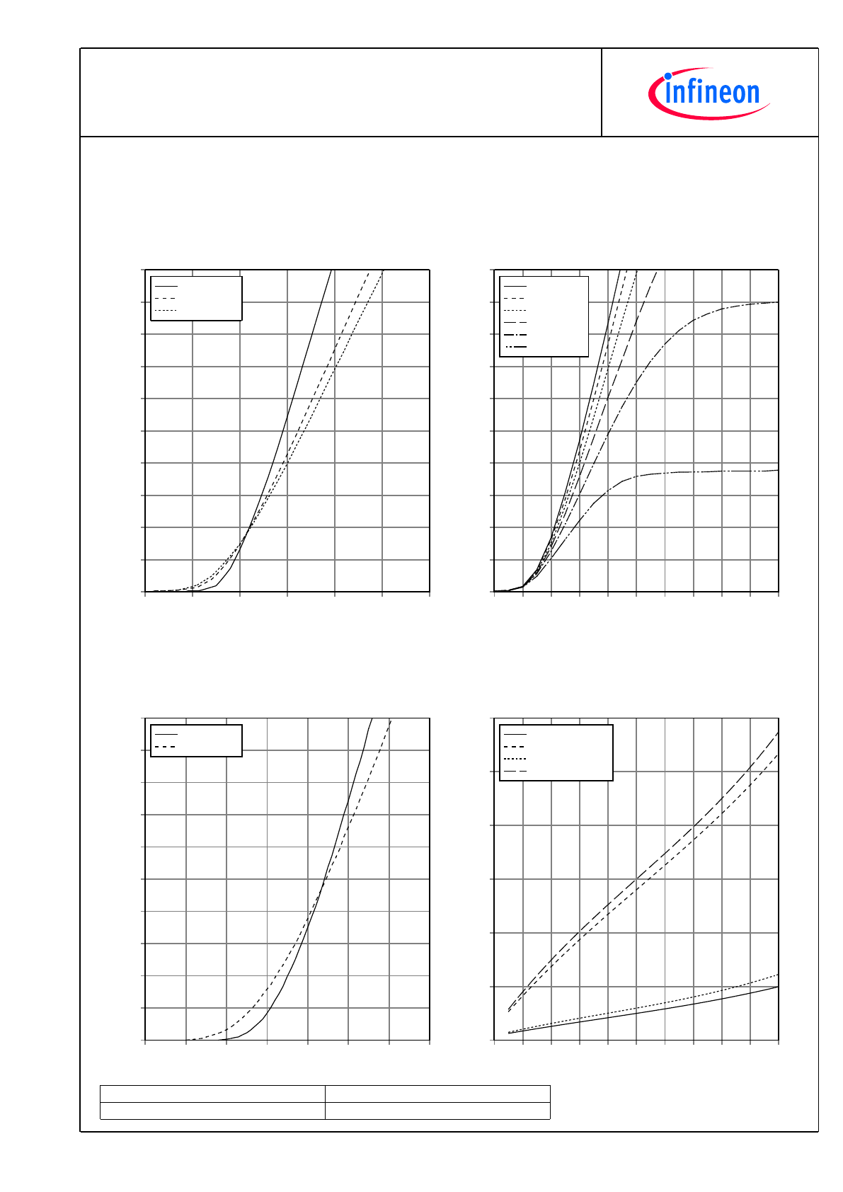
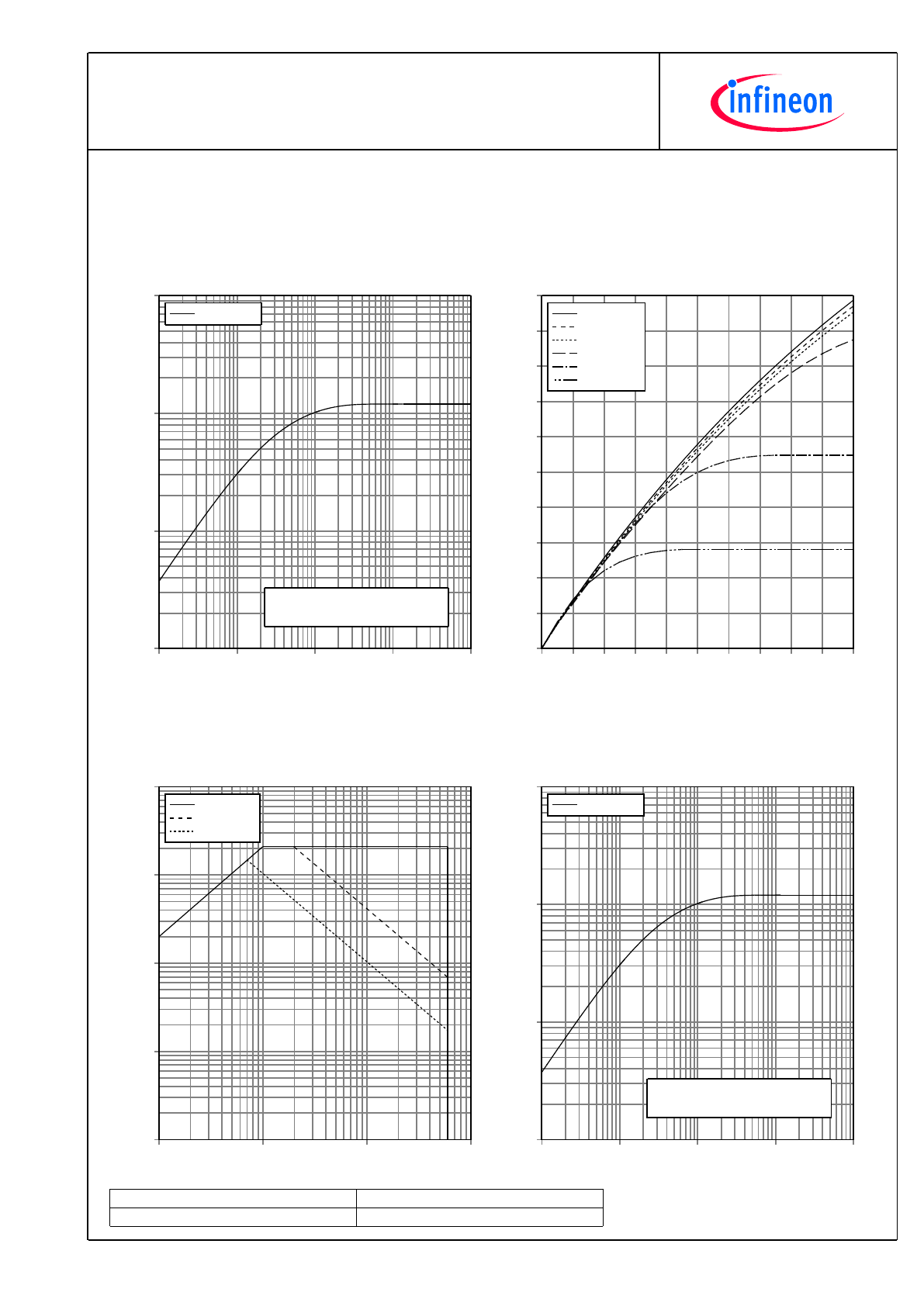
AusgangskennlinieIGBT,Wechselrichter(typisch)
outputcharacteristicIGBT,Inverter(typical)
I
C
=f(V
CE
)
V
GE
=15V
V
CE
[V]
I
C
[A]
0,0
0,5
1,0
1,5
2,0
2,5
3,0
0
15
30
45
60
75
90
105
120
135
150
T
vj
= 25°C
T
vj
= 125°C
T
vj
= 150°C
AusgangskennlinienfeldIGBT,Wechselrichter(typisch)
outputcharacteristicIGBT,Inverter(typical)
I
C
=f(V
CE
)
T
vj
=150°C
V
CE
[V]
I
C
[A]
0,0
0,5
1,0
1,5
2,0
2,5
3,0
3,5
4,0
4,5
5,0
0
15
30
45
60
75
90
105
120
135
150
V
GE
= 19 V
V
GE
= 17V
V
GE
= 15V
V
GE
= 13V
V
GE
= 11V
V
GE
= 9V
ÜbertragungscharakteristikIGBT,Wechselrichter(typisch)
transfercharacteristicIGBT,Inverter(typical)
I
C
=f(V
GE
)
V
CE
=20V
V
GE
[V]
I
C
[A]
5
6
7
8
9
10
11
12
0
15
30
45
60
75
90
105
120
135
150
T
vj
= 25°C
T
vj
= 125°C
SchaltverlusteIGBT,Wechselrichter(typisch)
switchinglossesIGBT,Inverter(typical)
E
on
=f(I
C
),E
off
=f(I
C
)
V
GE
=±15V,R
Gon
=5.1
Ω
,R
Goff
=5.1
Ω
,V
CE
=300V
I
C
[A]
E [mJ]
0
15
30
45
60
75
90
105 120 135 150
0
1
2
3
4
5
6
E
on
, T
vj
= 125°C
E
off
, T
vj
= 125°C
E
on
, T
vj
= 150°C
E
off
, T
vj
= 150°C
8
TechnischeInformation/TechnicalInformation
F5-75R06KE3_B5
IGBT-Module
IGBT-modules
preparedby:CM
approvedby:RS
dateofpublication:2013-11-04
revision:2.2
VorläufigeDaten
PreliminaryData
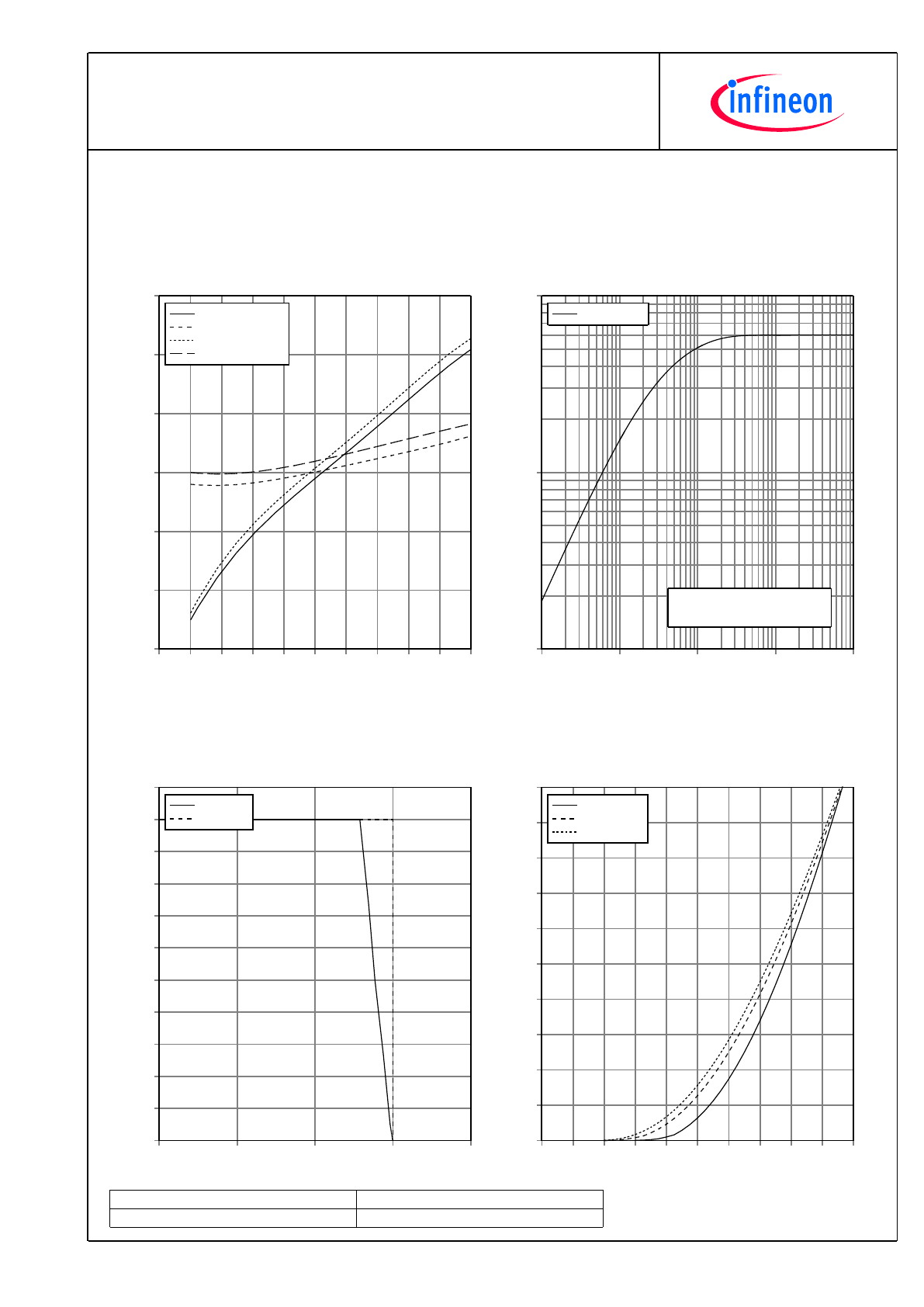
SchaltverlusteIGBT,Wechselrichter(typisch)
switchinglossesIGBT,Inverter(typical)
E
on
=f(R
G
),E
off
=f(R
G
)
V
GE
=±15V,I
C
=75A,V
CE
=300V
R
G
[
Ω
]
E [mJ]
0
5
10
15
20
25
30
35
40
45
50
0
1
2
3
4
5
6
E
on
, T
vj
= 125°C
E
off
, T
vj
= 125°C
E
on
, T
vj
= 150°C
E
off
, T
vj
= 150°C
TransienterWärmewiderstandIGBT,Wechselrichter
transientthermalimpedanceIGBT,Inverter
Z
thJC
=f(t)
t [s]
Z
thJC
[K/W]
0,001
0,01
0,1
1
10
0,01
0,1
1
Z
thJC
: IGBT
i:
r
i
[K/W]:
τ
i
[s]:
1
0,036
0,01
2
0,198
0,02
3
0,192
0,05
4
0,174
0,1
SichererRückwärts-ArbeitsbereichIGBT,Wechselrichter
(RBSOA)
reversebiassafeoperatingareaIGBT,Inverter(RBSOA)
I
C
=f(V
CE
)
V
GE
=±15V,R
Goff
=5.1
Ω
,T
vj
=150°C
V
CE
[V]
I
C
[A]
0
200
400
600
800
0
15
30
45
60
75
90
105
120
135
150
165
I
C
, Modul
I
C
, Chip
DurchlasskennliniederDiode,Wechselrichter(typisch)
forwardcharacteristicofDiode,Inverter(typical)
I
F
=f(V
F
)
V
F
[V]
I
F
[A]
0,0
0,2
0,4
0,6
0,8
1,0
1,2
1,4
1,6
1,8
2,0
0
15
30
45
60
75
90
105
120
135
150
T
vj
= 25°C
T
vj
= 125°C
T
vj
= 150°C
9
TechnischeInformation/TechnicalInformation
F5-75R06KE3_B5
IGBT-Module
IGBT-modules
preparedby:CM
approvedby:RS
dateofpublication:2013-11-04
revision:2.2
VorläufigeDaten
PreliminaryData
SchaltverlusteDiode,Wechselrichter(typisch)
switchinglossesDiode,Inverter(typical)
E
rec
=f(I
F
)
R
Gon
=5.1
Ω
,V
CE
=300V
I
F
[A]
E [mJ]
0
15
30
45
60
75
90
105 120 135 150
0,0
0,5
1,0
1,5
2,0
2,5
3,0
3,5
4,0
E
rec
, T
vj
= 125°C
E
rec
, T
vj
= 150°C
SchaltverlusteDiode,Wechselrichter(typisch)
switchinglossesDiode,Inverter(typical)
E
rec
=f(R
G
)
I
F
=75A,V
CE
=300V
R
G
[
Ω
]
E [mJ]
0
5
10
15
20
25
30
35
40
45
50
0,0
0,5
1,0
1,5
2,0
2,5
3,0
E
rec
, T
vj
= 125°C
E
rec
, T
vj
= 150°C
TransienterWärmewiderstandDiode,Wechselrichter
transientthermalimpedanceDiode,Inverter
Z
thJC
=f(t)
t [s]
Z
thJC
[K/W]
0,001
0,01
0,1
1
10
0,01
0,1
1
Z
thJC
: Diode
i:
r
i
[K/W]:
τ
i
[s]:
1
0,057
0,01
2
0,3135
0,02
3
0,304
0,05
4
0,2755
0,1
SichererArbeitsbereichMOSFET(SOA)
safeoperatingareaMOSFET(SOA)
I
D
=f(V
DS
)
V
GS
=±15V,T
c
=25°C
V
DS
[V]
I
D
[A]
1
10
100
1000
0,1
1
10
100
1000
t
P
= 100µs
t
P
= 10ms
DC
10
TechnischeInformation/TechnicalInformation
F5-75R06KE3_B5
IGBT-Module
IGBT-modules
preparedby:CM
approvedby:RS
dateofpublication:2013-11-04
revision:2.2
VorläufigeDaten
PreliminaryData
TransienterWärmewiderstandMOSFET
transientthermalimpedanceMOSFET
Z
thJC
=f(t)
t [s]
Z
thJC
[K/W]
0,001
0,01
0,1
1
10
0,001
0,01
0,1
1
Z
th
: Mosfet
i:
r
i
[K/W]:
τ
i
[s]:
1
0,0072
0,01
2
0,0396
0,02
3
0,0384
0,05
4
0,0348
0,1
AusgangskennlinieMOSFET(typisch)
outputcharacteristicMOSFET(typical)
I
D
=f(V
DS
)
T
vj
=125°C
V
DS
[V]
I
D
[A]
0
1
2
3
4
5
6
7
8
9
10
0
20
40
60
80
100
120
140
160
180
200
V
GS
= 20V
V
GS
= 10V
V
GS
= 8V
V
GS
= 7V
V
GS
= 6,5V
V
GS
= 6V
SichererArbeitsbereichMOSFETOVP-Zweig(SOA)
safeoperatingareaMOSFETOVP-Path(SOA)
I
D
=f(V
DS
)
V
GS
=±15V,T
c
=25°C
V
DS
[V]
I
D
[A]
1
10
100
1000
0,1
1
10
100
1000
t
P
= 100µs
t
P
= 10ms
DC
TransienterWärmewiderstandMOSFETOVP-Zweig
transientthermalimpedanceMOSFETOVP-Path
Z
thJC
=f(t)
t [s]
Z
thJC
[K/W]
0,001
0,01
0,1
1
10
0,001
0,01
0,1
1
Z
th
: Mosfet
i:
r
i
[K/W]:
τ
i
[s]:
1
0,0072
0,01
2
0,0396
0,02
3
0,0384
0,05
4
0,0348
0,1