
1
TechnischeInformation/TechnicalInformation
F3L75R07W2E3_B11
IGBT-Module
IGBT-modules
preparedby:DK
approvedby:MB
dateofpublication:2013-11-05
revision:2.1
ULapproved(E83335)
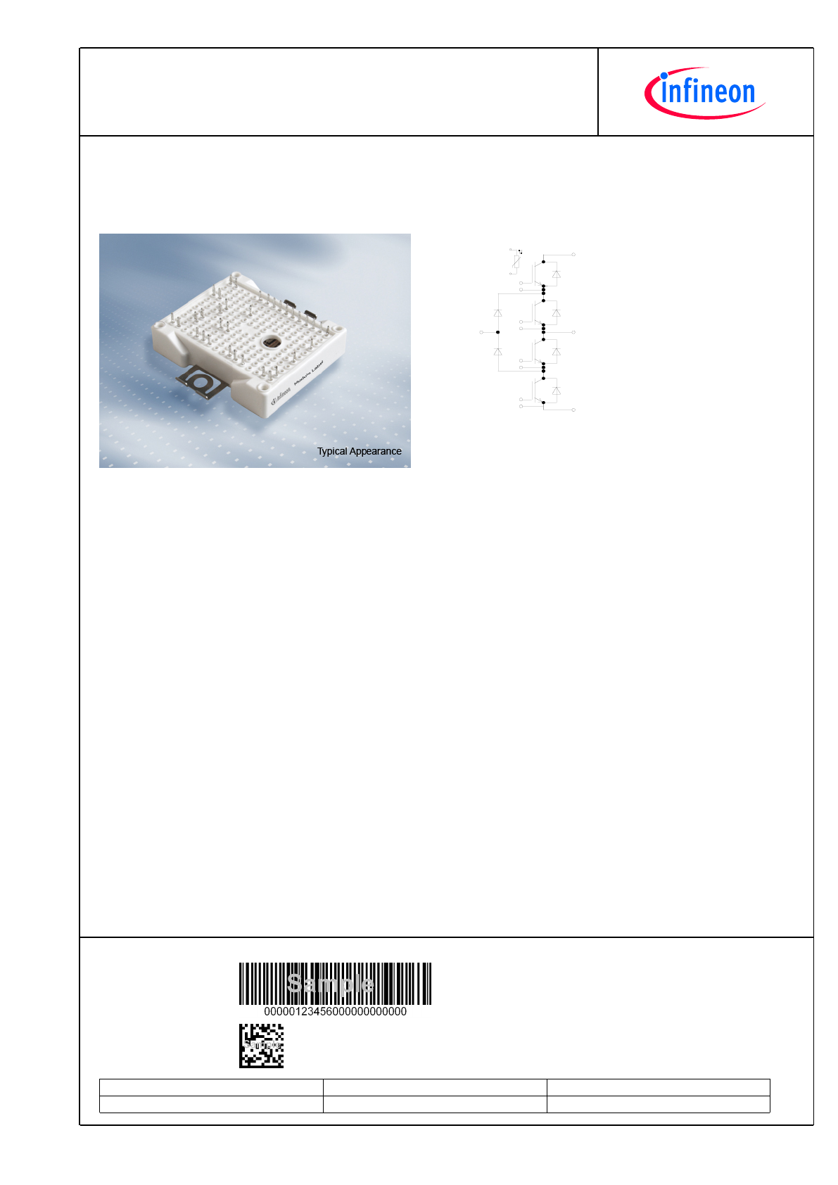
EasyPACKModulmitTrench/FeldstoppIGBT3undEmitterControlled3DiodeundPressFIT/NTC
EasyPACKmodulewithTrench/FieldstopIGBT3andEmitterControlled3diodeandPressFIT/NTC
VorläufigeDaten/PreliminaryData
J
V
CES
= 650V
I
C nom
= 75A / I
CRM
= 150A
TypischeAnwendungen
TypicalApplications
•
•
3-Level-Applikationen
3-Level-Applications
•
•
SolarAnwendungen
SolarApplications
•
•
USV-Systeme
UPSSystems
ElektrischeEigenschaften
ElectricalFeatures
•
•
ErhöhteSperrspannungsfestigkeitauf650V
Increasedblockingvoltagecapabilityto650V
•
•
NiederinduktivesDesign
Lowinductivedesign
•
•
NiedrigeSchaltverluste
LowSwitchingLosses
•
•
NiedrigesV
CEsat
LowV
CEsat
MechanischeEigenschaften
MechanicalFeatures
•
•
Al
2
O
3
Substrat mit kleinem thermischen
Widerstand
Al
2
O
3
SubstratewithLowThermalResistance
•
•
KompaktesDesign
Compactdesign
•
•
PressFITVerbindungstechnik
PressFITContactTechnology
•
•
Robuste Montage durch integrierte
Befestigungsklammern
Rugged mounting due to integrated mounting
clamps
ModuleLabelCode
BarcodeCode128
DMX-Code
ContentoftheCode
Digit
ModuleSerialNumber
1-5
ModuleMaterialNumber
6-11
ProductionOrderNumber
12-19
Datecode(ProductionYear)
20-21
Datecode(ProductionWeek)
22-23
2
TechnischeInformation/TechnicalInformation
F3L75R07W2E3_B11
IGBT-Module
IGBT-modules
preparedby:DK
approvedby:MB
dateofpublication:2013-11-05
revision:2.1
VorläufigeDaten
PreliminaryData
IGBT,Wechselrichter/IGBT,Inverter
HöchstzulässigeWerte/MaximumRatedValues
Kollektor-Emitter-Sperrspannung
Collector-emittervoltage
T
vj
= 25°C
V
CES
650
V
Kollektor-Dauergleichstrom
ContinuousDCcollectorcurrent
T
C
= 75°C, T
vj max
= 175°C
T
C
= 25°C, T
vj max
= 175°C
I
C nom
I
C
75
95
A
A
PeriodischerKollektor-Spitzenstrom
Repetitivepeakcollectorcurrent
t
P
= 1 ms
I
CRM
150
A
Gesamt-Verlustleistung
Totalpowerdissipation
T
C
= 25°C, T
vj max
= 175°C
P
tot
250
W
Gate-Emitter-Spitzenspannung
Gate-emitterpeakvoltage
V
GES
+/-20
V
CharakteristischeWerte/CharacteristicValues
min.
typ.
max.
Kollektor-Emitter-Sättigungsspannung
Collector-emittersaturationvoltage
I
C
= 75 A, V
GE
= 15 V
I
C
= 75 A, V
GE
= 15 V
I
C
= 75 A, V
GE
= 15 V
V
CE sat
1,45
1,60
1,70
1,90
V
V
V
T
vj
= 25°C
T
vj
= 125°C
T
vj
= 150°C
Gate-Schwellenspannung
Gatethresholdvoltage
I
C
= 1,20 mA, V
CE
= V
GE
, T
vj
= 25°C
V
GEth
4,9
5,8
6,5
V
Gateladung
Gatecharge
V
GE
= -15 V ... +15 V
Q
G
0,80
µC
InternerGatewiderstand
Internalgateresistor
T
vj
= 25°C
R
Gint
0,0
Ω
Eingangskapazität
Inputcapacitance
f = 1 MHz, T
vj
= 25°C, V
CE
= 25 V, V
GE
= 0 V
C
ies
4,60
nF
Rückwirkungskapazität
Reversetransfercapacitance
f = 1 MHz, T
vj
= 25°C, V
CE
= 25 V, V
GE
= 0 V
C
res
0,145
nF
Kollektor-Emitter-Reststrom
Collector-emittercut-offcurrent
V
CE
= 650 V, V
GE
= 0 V, T
vj
= 25°C
I
CES
1,0
mA
Gate-Emitter-Reststrom
Gate-emitterleakagecurrent
V
CE
= 0 V, V
GE
= 20 V, T
vj
= 25°C
I
GES
400
nA
Einschaltverzögerungszeit,induktiveLast
Turn-ondelaytime,inductiveload
I
C
= 75 A, V
CE
= 300 V
V
GE
= ±15 V
R
Gon
= 5,1
Ω
t
d on
0,025
0,025
0,025
µs
µs
µs
T
vj
= 25°C
T
vj
= 125°C
T
vj
= 150°C
Anstiegszeit,induktiveLast
Risetime,inductiveload
I
C
= 75 A, V
CE
= 300 V
V
GE
= ±15 V
R
Gon
= 5,1
Ω
t
r
0,02
0,023
0,024
µs
µs
µs
T
vj
= 25°C
T
vj
= 125°C
T
vj
= 150°C
Abschaltverzögerungszeit,induktiveLast
Turn-offdelaytime,inductiveload
I
C
= 75 A, V
CE
= 300 V
V
GE
= ±15 V
R
Goff
= 5,1
Ω
t
d off
0,20
0,225
0,23
µs
µs
µs
T
vj
= 25°C
T
vj
= 125°C
T
vj
= 150°C
Fallzeit,induktiveLast
Falltime,inductiveload
I
C
= 75 A, V
CE
= 300 V
V
GE
= ±15 V
R
Goff
= 5,1
Ω
t
f
0,085
0,12
0,14
µs
µs
µs
T
vj
= 25°C
T
vj
= 125°C
T
vj
= 150°C
EinschaltverlustenergieproPuls
Turn-onenergylossperpulse
I
C
= 75 A, V
CE
= 300 V, L
S
= 35 nH
V
GE
= ±15 V, di/dt = 3100 A/µs (T
vj
= 150°C)
R
Gon
= 5,1
Ω
E
on
0,45
0,60
0,70
mJ
mJ
mJ
T
vj
= 25°C
T
vj
= 125°C
T
vj
= 150°C
AbschaltverlustenergieproPuls
Turn-offenergylossperpulse
I
C
= 75 A, V
CE
= 300 V, L
S
= 35 nH
V
GE
= ±15 V, du/dt = 4000 V/µs (T
vj
= 150°C)
R
Goff
= 5,1
Ω
E
off
1,70
2,30
2,40
mJ
mJ
mJ
T
vj
= 25°C
T
vj
= 125°C
T
vj
= 150°C
Kurzschlußverhalten
SCdata
V
GE
≤
15 V, V
CC
= 360 V
V
CEmax
= V
CES
-L
sCE
·di/dt
I
SC
530
380
A
A
T
vj
= 25°C
T
vj
= 150°C
t
P
≤
8 µs,
t
P
≤
6 µs,
Wärmewiderstand,ChipbisGehäuse
Thermalresistance,junctiontocase
proIGBT/perIGBT
R
thJC
0,55
0,60
K/W
Wärmewiderstand,GehäusebisKühlkörper
Thermalresistance,casetoheatsink
proIGBT/perIGBT
λ
Paste
=1W/(m·K)/
λ
grease
=1W/(m·K)
R
thCH
0,55
K/W
TemperaturimSchaltbetrieb
Temperatureunderswitchingconditions
T
vj op
-40
150
°C
3
TechnischeInformation/TechnicalInformation
F3L75R07W2E3_B11
IGBT-Module
IGBT-modules
preparedby:DK
approvedby:MB
dateofpublication:2013-11-05
revision:2.1
VorläufigeDaten
PreliminaryData
Diode,Wechselrichter/Diode,Inverter
HöchstzulässigeWerte/MaximumRatedValues
PeriodischeSpitzensperrspannung
Repetitivepeakreversevoltage
T
vj
= 25°C
V
RRM
650
V
Dauergleichstrom
ContinuousDCforwardcurrent
I
F
75
A
PeriodischerSpitzenstrom
Repetitivepeakforwardcurrent
t
P
= 1 ms
I
FRM
150
A
Grenzlastintegral
I²t-value
V
R
= 0 V, t
P
= 10 ms, T
vj
= 125°C
V
R
= 0 V, t
P
= 10 ms, T
vj
= 150°C
I²t
490
460
A²s
A²s
CharakteristischeWerte/CharacteristicValues
min.
typ.
max.
Durchlassspannung
Forwardvoltage
I
F
= 75 A, V
GE
= 0 V
I
F
= 75 A, V
GE
= 0 V
I
F
= 75 A, V
GE
= 0 V
V
F
1,55
1,50
1,45
1,95
V
V
V
T
vj
= 25°C
T
vj
= 125°C
T
vj
= 150°C
Rückstromspitze
Peakreverserecoverycurrent
I
F
= 75 A, - di
F
/dt = 3600 A/µs (T
vj
=150°C)
V
R
= 300 V
V
GE
= -15 V
I
RM
95,0
105
110
A
A
A
T
vj
= 25°C
T
vj
= 125°C
T
vj
= 150°C
Sperrverzögerungsladung
Recoveredcharge
I
F
= 75 A, - di
F
/dt = 3600 A/µs (T
vj
=150°C)
V
R
= 300 V
V
GE
= -15 V
Q
r
3,70
6,40
7,00
µC
µC
µC
T
vj
= 25°C
T
vj
= 125°C
T
vj
= 150°C
AbschaltenergieproPuls
Reverserecoveryenergy
I
F
= 75 A, - di
F
/dt = 3600 A/µs (T
vj
=150°C)
V
R
= 300 V
V
GE
= -15 V
E
rec
0,90
1,50
1,75
mJ
mJ
mJ
T
vj
= 25°C
T
vj
= 125°C
T
vj
= 150°C
Wärmewiderstand,ChipbisGehäuse
Thermalresistance,junctiontocase
proDiode/perdiode
R
thJC
0,70
0,80
K/W
Wärmewiderstand,GehäusebisKühlkörper
Thermalresistance,casetoheatsink
proDiode/perdiode
λ
Paste
=1W/(m·K)/
λ
grease
=1W/(m·K)
R
thCH
0,70
K/W
TemperaturimSchaltbetrieb
Temperatureunderswitchingconditions
T
vj op
-40
150
°C
4
TechnischeInformation/TechnicalInformation
F3L75R07W2E3_B11
IGBT-Module
IGBT-modules
preparedby:DK
approvedby:MB
dateofpublication:2013-11-05
revision:2.1
VorläufigeDaten
PreliminaryData
Diode,D5-D6/Diode,D5-D6
HöchstzulässigeWerte/MaximumRatedValues
PeriodischeSpitzensperrspannung
Repetitivepeakreversevoltage
T
vj
= 25°C
V
RRM
650
V
Dauergleichstrom
ContinuousDCforwardcurrent
I
F
75
A
PeriodischerSpitzenstrom
Repetitivepeakforwardcurrent
t
P
= 1 ms
I
FRM
150
A
Grenzlastintegral
I²t-value
V
R
= 0 V, t
P
= 10 ms, T
vj
= 125°C
V
R
= 0 V, t
P
= 10 ms, T
vj
= 150°C
I²t
1500
1400
A²s
A²s
CharakteristischeWerte/CharacteristicValues
min.
typ.
max.
Durchlassspannung
Forwardvoltage
I
F
= 75 A, V
GE
= 0 V
I
F
= 75 A, V
GE
= 0 V
I
F
= 75 A, V
GE
= 0 V
V
F
1,45
1,35
1,30
1,85
V
V
V
T
vj
= 25°C
T
vj
= 125°C
T
vj
= 150°C
Rückstromspitze
Peakreverserecoverycurrent
I
F
= 75 A, - di
F
/dt = 3100 A/µs (T
vj
=150°C)
V
R
= 300 V
I
RM
82,0
100
105
A
A
A
T
vj
= 25°C
T
vj
= 125°C
T
vj
= 150°C
Sperrverzögerungsladung
Recoveredcharge
I
F
= 75 A, - di
F
/dt = 3100 A/µs (T
vj
=150°C)
V
R
= 300 V
Q
r
3,70
7,00
8,00
µC
µC
µC
T
vj
= 25°C
T
vj
= 125°C
T
vj
= 150°C
AbschaltenergieproPuls
Reverserecoveryenergy
I
F
= 75 A, - di
F
/dt = 3100 A/µs (T
vj
=150°C)
V
R
= 300 V
E
rec
1,00
1,80
2,05
mJ
mJ
mJ
T
vj
= 25°C
T
vj
= 125°C
T
vj
= 150°C
Wärmewiderstand,ChipbisGehäuse
Thermalresistance,junctiontocase
proDiode/perdiode
R
thJC
0,60
0,65
K/W
Wärmewiderstand,GehäusebisKühlkörper
Thermalresistance,casetoheatsink
proDiode/perdiode
λ
Paste
=1W/(m·K)/
λ
grease
=1W/(m·K)
R
thCH
0,50
K/W
TemperaturimSchaltbetrieb
Temperatureunderswitchingconditions
T
vj op
-40
150
°C
NTC-Widerstand/NTC-Thermistor
CharakteristischeWerte/CharacteristicValues
min.
typ.
max.
Nennwiderstand
Ratedresistance
T
C
= 25°C
R
25
5,00
k
Ω
AbweichungvonR100
DeviationofR100
T
C
= 100°C, R
100
= 493
Ω
∆
R/R
-5
5
%
Verlustleistung
Powerdissipation
T
C
= 25°C
P
25
20,0
mW
B-Wert
B-value
R
2
= R
25
exp [B
25/50
(1/T
2
- 1/(298,15 K))]
B
25/50
3375
K
B-Wert
B-value
R
2
= R
25
exp [B
25/80
(1/T
2
- 1/(298,15 K))]
B
25/80
3411
K
B-Wert
B-value
R
2
= R
25
exp [B
25/100
(1/T
2
- 1/(298,15 K))]
B
25/100
3433
K
AngabengemäßgültigerApplicationNote.
Specificationaccordingtothevalidapplicationnote.
5
TechnischeInformation/TechnicalInformation
F3L75R07W2E3_B11
IGBT-Module
IGBT-modules
preparedby:DK
approvedby:MB
dateofpublication:2013-11-05
revision:2.1
VorläufigeDaten
PreliminaryData
Modul/Module
Isolations-Prüfspannung
Isolationtestvoltage
RMS, f = 50 Hz, t = 1 min.
V
ISOL
2,5
kV
InnereIsolation
Internalisolation
Basisisolierung(Schutzklasse1,EN61140)
basicinsulation(class1,IEC61140)
Al
2
O
3
Kriechstrecke
Creepagedistance
Kontakt-Kühlkörper/terminaltoheatsink
Kontakt-Kontakt/terminaltoterminal
11,5
6,3
mm
Luftstrecke
Clearance
Kontakt-Kühlkörper/terminaltoheatsink
Kontakt-Kontakt/terminaltoterminal
10,0
5,0
mm
VergleichszahlderKriechwegbildung
Comperativetrackingindex
CTI
> 200
min.
typ.
max.
Modulstreuinduktivität
Strayinductancemodule
L
sCE
15
nH
Modulleitungswiderstand,Anschlüsse-
Chip
Moduleleadresistance,terminals-chip
T
C
=25°C,proSchalter/perswitch
R
CC'+EE'
2,00
m
Ω
Lagertemperatur
Storagetemperature
T
stg
-40
125
°C
Anpresskraft für mech. Bef. pro Feder
mountig force per clamp
F
40
-
80
N
Gewicht
Weight
G
39
g
Der Strom im Dauerbetrieb ist auf 25 A effektiv pro Anschlusspin begrenzt
The current under continuous operation is limited to 25 A rms per connector pin
6
TechnischeInformation/TechnicalInformation
F3L75R07W2E3_B11
IGBT-Module
IGBT-modules
preparedby:DK
approvedby:MB
dateofpublication:2013-11-05
revision:2.1
VorläufigeDaten
PreliminaryData
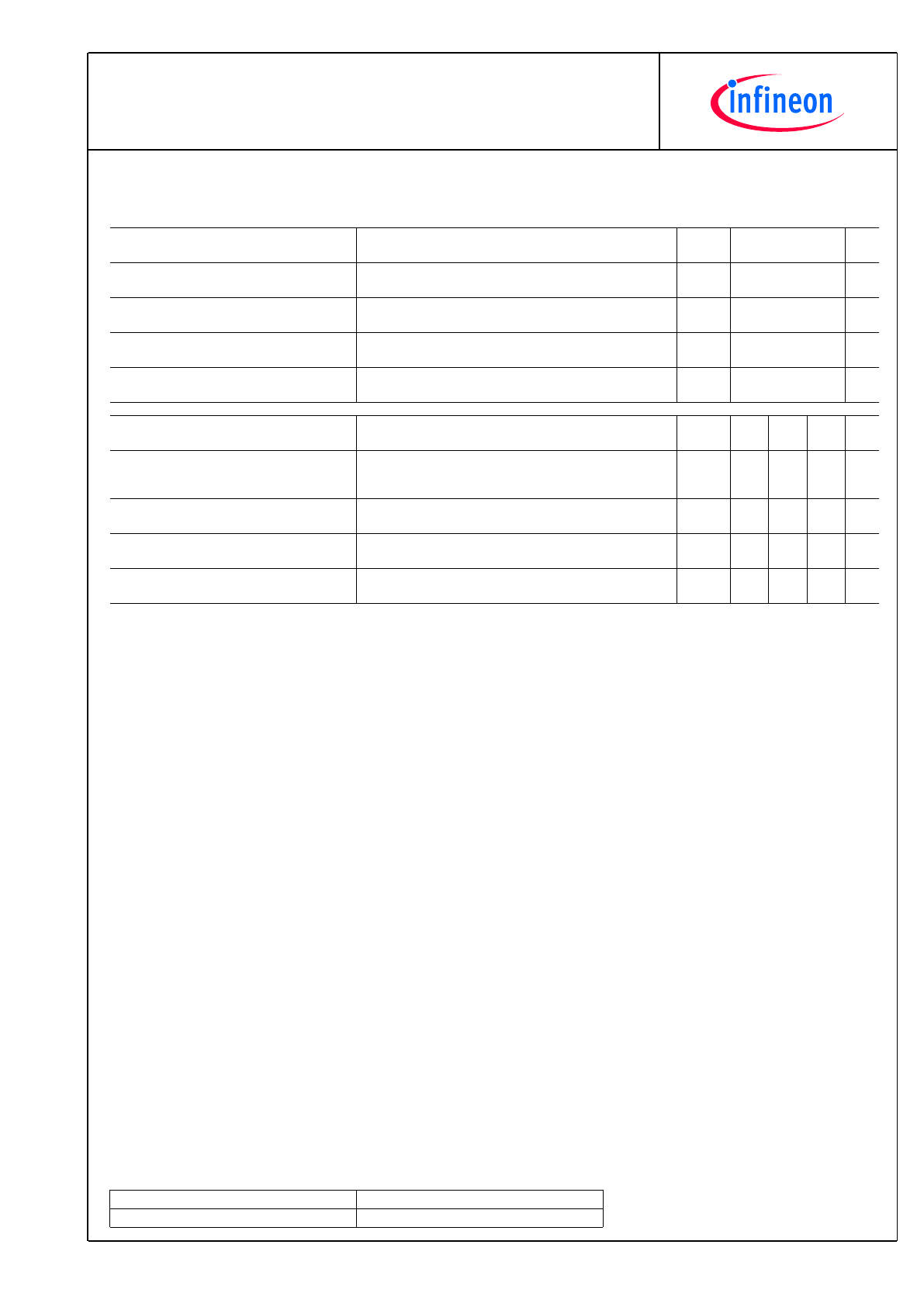
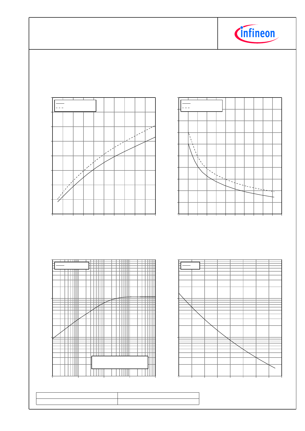
AusgangskennlinieIGBT,Wechselrichter(typisch)
outputcharacteristicIGBT,Inverter(typical)
I
C
=f(V
CE
)
V
GE
=15V
V
CE
[V]
I
C
[A]
0,0
0,4
0,8
1,2
1,6
2,0
2,4
2,8
0
15
30
45
60
75
90
105
120
135
150
T
vj
= 25°C
T
vj
= 125°C
T
vj
= 150°C
AusgangskennlinienfeldIGBT,Wechselrichter(typisch)
outputcharacteristicIGBT,Inverter(typical)
I
C
=f(V
CE
)
T
vj
=150°C
V
CE
[V]
I
C
[A]
0,0
0,5
1,0
1,5
2,0
2,5
3,0
3,5
4,0
4,5
5,0
0
15
30
45
60
75
90
105
120
135
150
V
GE
= 19V
V
GE
= 17V
V
GE
= 15V
V
GE
= 13V
V
GE
= 11V
V
GE
= 9V
ÜbertragungscharakteristikIGBT,Wechselrichter(typisch)
transfercharacteristicIGBT,Inverter(typical)
I
C
=f(V
GE
)
V
CE
=20V
V
GE
[V]
I
C
[A]
5
6
7
8
9
10
11
12
0
15
30
45
60
75
90
105
120
135
150
T
vj
= 25°C
T
vj
= 125°C
T
vj
= 150°C
SchaltverlusteIGBT,Wechselrichter(typisch)
switchinglossesIGBT,Inverter(typical)
E
on
=f(I
C
),E
off
=f(I
C
)
V
GE
=±15V,R
Gon
=5.1
Ω
,R
Goff
=5.1
Ω
,V
CE
=300V
I
C
[A]
E [mJ]
0
15
30
45
60
75
90
105 120 135 150
0,0
0,5
1,0
1,5
2,0
2,5
3,0
3,5
4,0
4,5
5,0
E
on
, T
vj
= 125°C
E
off
, T
vj
= 125°C
E
on
, T
vj
= 150°C
E
off
, T
vj
= 150°C
7
TechnischeInformation/TechnicalInformation
F3L75R07W2E3_B11
IGBT-Module
IGBT-modules
preparedby:DK
approvedby:MB
dateofpublication:2013-11-05
revision:2.1
VorläufigeDaten
PreliminaryData
SchaltverlusteIGBT,Wechselrichter(typisch)
switchinglossesIGBT,Inverter(typical)
E
on
=f(R
G
),E
off
=f(R
G
)
V
GE
=±15V,I
C
=75A,V
CE
=300V
R
G
[
Ω
]
E [mJ]
0
5
10
15
20
25
30
35
40
45
50
55
0
1
2
3
4
5
6
7
8
9
10
E
on
, T
vj
= 125°C
E
off
, T
vj
= 125°C
E
on
, T
vj
= 150°C
E
off
, T
vj
= 150°C
TransienterWärmewiderstandIGBT,Wechselrichter
transientthermalimpedanceIGBT,Inverter
Z
thJH
=f(t)
t [s]
Z
thJH
[K/W]
0,001
0,01
0,1
1
10
0,01
0,1
1
10
Z
thJH
: IGBT
i:
r
i
[K/W]:
τ
i
[s]:
1
0,051
0,0005
2
0,117
0,005
3
0,426
0,05
4
0,506
0,2
SichererRückwärts-ArbeitsbereichIGBT,Wechselrichter
(RBSOA)
reversebiassafeoperatingareaIGBT,Inverter(RBSOA)
I
C
=f(V
CE
)
V
GE
=±15V,R
Goff
=5.1
Ω
,T
vj
=150°C
V
CE
[V]
I
C
[A]
0
100
200
300
400
500
600
700
800
0
15
30
45
60
75
90
105
120
135
150
165
I
C
, Modul
I
C
, Chip
DurchlasskennliniederDiode,Wechselrichter(typisch)
forwardcharacteristicofDiode,Inverter(typical)
I
F
=f(V
F
)
V
F
[V]
I
F
[A]
0,0
0,4
0,8
1,2
1,6
2,0
2,4
0
15
30
45
60
75
90
105
120
135
150
T
vj
= 25°C
T
vj
= 125°C
T
vj
= 150°C
8
TechnischeInformation/TechnicalInformation
F3L75R07W2E3_B11
IGBT-Module
IGBT-modules
preparedby:DK
approvedby:MB
dateofpublication:2013-11-05
revision:2.1
VorläufigeDaten
PreliminaryData
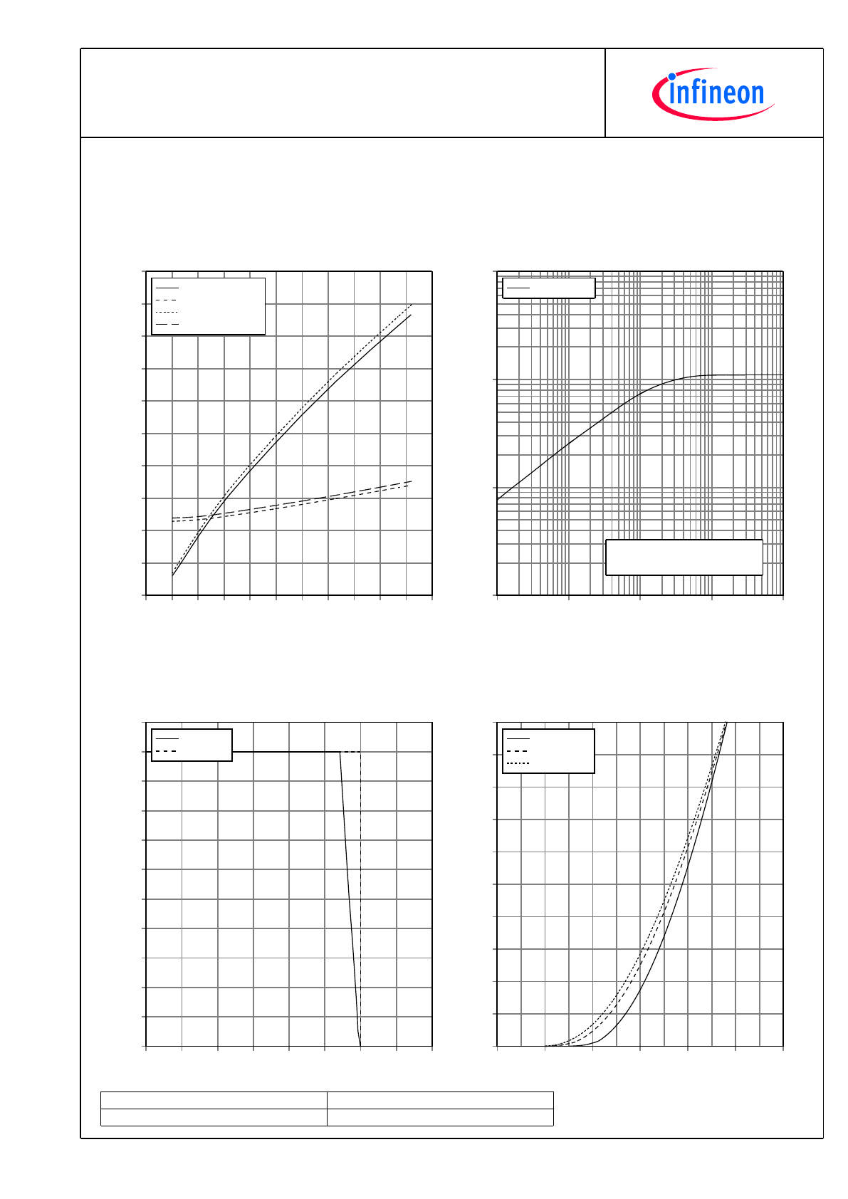
SchaltverlusteDiode,Wechselrichter(typisch)
switchinglossesDiode,Inverter(typical)
E
rec
=f(I
F
)
R
Gon
=5.1
Ω
,V
CE
=300V
I
F
[A]
E [mJ]
0
15
30
45
60
75
90
105 120 135 150
0,0
0,5
1,0
1,5
2,0
2,5
3,0
3,5
4,0
E
rec
, T
vj
= 125°C
E
rec
, T
vj
= 150°C
SchaltverlusteDiode,Wechselrichter(typisch)
switchinglossesDiode,Inverter(typical)
E
rec
=f(R
G
)
I
F
=75A,V
CE
=300V
R
G
[
Ω
]
E [mJ]
0
5
10
15
20
25
30
35
40
45
50
55
0,0
0,5
1,0
1,5
2,0
2,5
3,0
E
rec
, T
vj
= 125°C
E
rec
, T
vj
= 150°C
TransienterWärmewiderstandDiode,Wechselrichter
transientthermalimpedanceDiode,Inverter
Z
thJH
=f(t)
t [s]
Z
thJH
[K/W]
0,001
0,01
0,1
1
10
0,1
1
10
Z
thJH
: Diode
i:
r
i
[K/W]:
τ
i
[s]:
1
0,097
0,0005
2
0,219
0,005
3
0,576
0,05
4
0,508
0,2
DurchlasskennliniederDiode,D5-D6(typisch)
forwardcharacteristicofDiode,D5-D6(typical)
I
F
=f(V
F
)
V
F
[V]
I
F
[A]
0,0
0,4
0,8
1,2
1,6
2,0
0
15
30
45
60
75
90
105
120
135
150
T
vj
= 25°C
T
vj
= 125°C
T
vj
= 150°C
9
TechnischeInformation/TechnicalInformation
F3L75R07W2E3_B11
IGBT-Module
IGBT-modules
preparedby:DK
approvedby:MB
dateofpublication:2013-11-05
revision:2.1
VorläufigeDaten
PreliminaryData
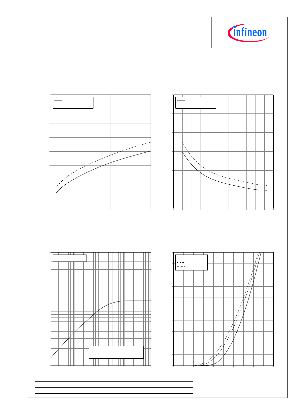
SchaltverlusteDiode,D5-D6(typisch)
switchinglossesDiode,D5-D6(typical)
E
rec
=f(I
F
)
R
Gon
=5.1
Ω
,V
CE
=300V
I
F
[A]
E [mJ]
0
15
30
45
60
75
90
105 120 135 150
0,0
0,5
1,0
1,5
2,0
2,5
3,0
3,5
4,0
E
rec
, T
vj
= 125°C
E
rec
, T
vj
= 150°C
SchaltverlusteDiode,D5-D6(typisch)
switchinglossesDiode,D5-D6(typical)
E
rec
=f(R
G
)
I
F
=75A,V
CE
=300V
R
G
[
Ω
]
E [mJ]
0
5
10
15
20
25
30
35
40
45
50
55
0,0
0,3
0,6
0,9
1,2
1,5
1,8
2,1
2,4
2,7
3,0
E
rec
, T
vj
= 125°C
E
rec
, T
vj
= 150°C
TransienterWärmewiderstandDiode,D5-D6
transientthermalimpedanceDiode,D5-D6
Z
thJH
=f(t)
t [s]
Z
thJH
[K/W]
0,001
0,01
0,1
1
10
0,01
0,1
1
10
Z
thJH
: Diode
i:
r
i
[K/W]:
τ
i
[s]:
1
0,062
0,0005
2
0,145
0,005
3
0,444
0,05
4
0,449
0,2
NTC-Widerstand-Temperaturkennlinie(typisch)
NTC-Thermistor-temperaturecharacteristic(typical)
R=f(T)
T
C
[°C]
R[
Ω
]
0
20
40
60
80
100
120
140
160
100
1000
10000
100000
R
typ
10
TechnischeInformation/TechnicalInformation
F3L75R07W2E3_B11
IGBT-Module
IGBT-modules
preparedby:DK
approvedby:MB
dateofpublication:2013-11-05
revision:2.1
VorläufigeDaten
PreliminaryData
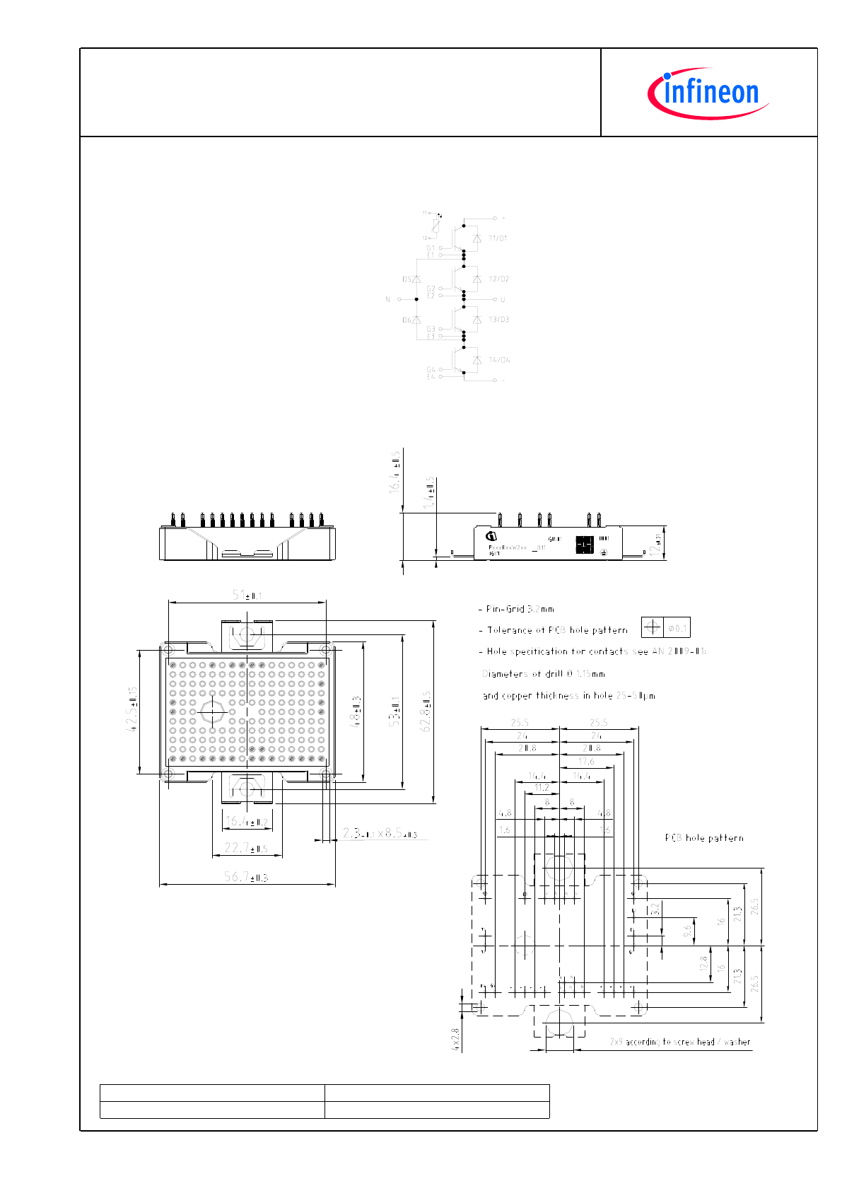
Schaltplan/circuit_diagram_headline
J
Gehäuseabmessungen/packageoutlines
In fin e o n