

IGBT
Highspeed5FASTIGBTinTRENCHSTOP
TM
5technologycopackedwithRAPID1
fastandsoftantiparalleldiode
IKP08N65F5
650VDuoPackIGBTandDiode
Highspeedswitchingseriesfifthgeneration
Datasheet
IndustrialPowerControl
2
IKP08N65F5
Highspeedswitchingseriesfifthgeneration
Rev.2.1,2015-05-05
Highspeed5FASTIGBTinTRENCHSTOP
TM
5technologycopackedwith
RAPID1fastandsoftantiparalleldiode
FeaturesandBenefits:
HighspeedF5technologyoffering
•Best-in-Classefficiencyinhardswitchingandresonant
topologies
•650Vbreakdownvoltage
•LowQ
G
•IGBTcopackedwithRAPID1fastandsoftantiparalleldiode
•Maximumjunctiontemperature175°C
•QualifiedaccordingtoJEDECfortargetapplications
•Pb-freeleadplating;RoHScompliant
•CompleteproductspectrumandPSpiceModels:
http://www.infineon.com/igbt/
Applications:
•Solarconverters
•Uninterruptiblepowersupplies
•Weldingconverters
•Midtohighrangeswitchingfrequencyconverters
G
C
E
G
C E
C
KeyPerformanceandPackageParameters
Type
V
CE
I
C
V
CEsat
,T
vj
=25°C
T
vjmax
Marking
Package
IKP08N65F5
650V
8A
1.6V
175°C
K08EEF5
PG-TO220-3

3
IKP08N65F5
Highspeedswitchingseriesfifthgeneration
Rev.2.1,2015-05-05
TableofContents
Description . . . . . . . . . . . . . . . . . . . . . . . . . . . . . . . . . . . . . . . . . . . . . . . . . . . . . . . . . . . . . . . . . . . . . . . . 2
Table of Contents . . . . . . . . . . . . . . . . . . . . . . . . . . . . . . . . . . . . . . . . . . . . . . . . . . . . . . . . . . . . . . . . . . . 3
Maximum Ratings . . . . . . . . . . . . . . . . . . . . . . . . . . . . . . . . . . . . . . . . . . . . . . . . . . . . . . . . . . . . . . . . . . . 4
Thermal Resistance . . . . . . . . . . . . . . . . . . . . . . . . . . . . . . . . . . . . . . . . . . . . . . . . . . . . . . . . . . . . . . . . . 4
Electrical Characteristics . . . . . . . . . . . . . . . . . . . . . . . . . . . . . . . . . . . . . . . . . . . . . . . . . . . . . . . . . . . . . . 5
Electrical Characteristics Diagrams . . . . . . . . . . . . . . . . . . . . . . . . . . . . . . . . . . . . . . . . . . . . . . . . . . . . . 8
Package Drawing . . . . . . . . . . . . . . . . . . . . . . . . . . . . . . . . . . . . . . . . . . . . . . . . . . . . . . . . . . . . . . . . . . .15
Testing Conditions . . . . . . . . . . . . . . . . . . . . . . . . . . . . . . . . . . . . . . . . . . . . . . . . . . . . . . . . . . . . . . . . . .16
Revision History . . . . . . . . . . . . . . . . . . . . . . . . . . . . . . . . . . . . . . . . . . . . . . . . . . . . . . . . . . . . . . . . . . . .17
Disclaimer . . . . . . . . . . . . . . . . . . . . . . . . . . . . . . . . . . . . . . . . . . . . . . . . . . . . . . . . . . . . . . . . . . . . . . . . .17

4
IKP08N65F5
Highspeedswitchingseriesfifthgeneration
Rev.2.1,2015-05-05
MaximumRatings
Foroptimumlifetimeandreliability,Infineonrecommendsoperatingconditionsthatdonotexceed80%ofthemaximumratingsstatedinthisdatasheet.
Parameter
Symbol
Value
Unit
Collector-emitter voltage
V
CE
650
V
DCcollectorcurrent,limitedbyT
vjmax
T
C
=25°C
T
C
=100°C
I
C
18.0
11.0
A
Pulsedcollectorcurrent,t
p
limitedbyT
vjmax
I
Cpuls
24.0
A
TurnoffsafeoperatingareaV
CE
≤
650V,T
vj
≤
175°C
-
24.0
A
Diodeforwardcurrent,limitedbyT
vjmax
T
C
=25°C
T
C
=100°C
I
F
20.0
12.0
A
Diodepulsedcurrent,t
p
limitedbyT
vjmax
I
Fpuls
24.0
A
Gate-emitter voltage
TransientGate-emittervoltage(t
p
≤
10µs,D<0.010)
V
GE
±20
±30
V
PowerdissipationT
C
=25°C
PowerdissipationT
C
=100°C
P
tot
70.0
35.0
W
Operating junction temperature
T
vj
-40...+175
°C
Storage temperature
T
stg
-55...+150
°C
Soldering temperature,
wave soldering 1.6mm (0.063in.) from case for 10s
260
°C
Mounting torque, M3 screw
Maximum of mounting processes: 3
M
0.6
Nm
ThermalResistance
Parameter
Symbol Conditions
Max.Value
Unit
Characteristic
IGBT thermal resistance,
junction - case
R
th(j-c)
2.20
K/W
Diode thermal resistance,
junction - case
R
th(j-c)
2.90
K/W
Thermal resistance
junction - ambient
R
th(j-a)
62
K/W

5
IKP08N65F5
Highspeedswitchingseriesfifthgeneration
Rev.2.1,2015-05-05
ElectricalCharacteristic,atT
vj
=25°C,unlessotherwisespecified
Value
min.
typ.
max.
Parameter
Symbol Conditions
Unit
StaticCharacteristic
Collector-emitter breakdown voltage
V
(BR)CES
V
GE
=0V,I
C
=0.20mA
650
-
-
V
Collector-emitter saturation voltage
V
CEsat
V
GE
=15.0V,I
C
=8.0A
T
vj
=25°C
T
vj
=125°C
T
vj
=175°C
-
-
-
1.60
1.80
1.90
2.10
-
-
V
Diode forward voltage
V
F
V
GE
=0V,I
F
=9.0A
T
vj
=25°C
T
vj
=125°C
T
vj
=175°C
-
-
-
1.45
1.40
1.40
1.80
-
-
V
Gate-emitter threshold voltage
V
GE(th)
I
C
=0.08mA,V
CE
=V
GE
3.2
4.0
4.8
V
Zero gate voltage collector current
I
CES
V
CE
=650V,V
GE
=0V
T
vj
=25°C
T
vj
=175°C
-
-
-
-
40.0
4000.0
µA
Gate-emitter leakage current
I
GES
V
CE
=0V,V
GE
=20V
-
-
100
nA
Transconductance
g
fs
V
CE
=20V,I
C
=8.0A
-
17.0
-
S
ElectricalCharacteristic,atT
vj
=25°C,unlessotherwisespecified
Value
min.
typ.
max.
Parameter
Symbol Conditions
Unit
DynamicCharacteristic
Input capacitance
C
ies
-
500
-
Output capacitance
C
oes
-
16
-
Reverse transfer capacitance
C
res
-
3
-
V
CE
=25V,V
GE
=0V,f=1MHz
pF
Gate charge
Q
G
V
CC
=520V,I
C
=8.0A,
V
GE
=15V
-
22.0
-
nC
Internal emitter inductance
measured 5mm (0.197 in.) from
case
L
E
-
7.0
-
nH
SwitchingCharacteristic,InductiveLoad
Value
min.
typ.
max.
Parameter
Symbol Conditions
Unit
IGBTCharacteristic,atT
vj
=25°C
Turn-on delay time
t
d(on)
-
10
-
ns
Rise time
t
r
-
5
-
ns
Turn-off delay time
t
d(off)
-
116
-
ns
Fall time
t
f
-
20
-
ns
Turn-on energy
E
on
-
0.07
-
mJ
Turn-off energy
E
off
-
0.02
-
mJ
Total switching energy
E
ts
-
0.09
-
mJ
T
vj
=25°C,
V
CC
=400V,I
C
=4.0A,
V
GE
=0.0/15.0V,
R
G(on)
=48.0
Ω
,R
G(off)
=48.0
Ω
,
L
σ
=30nH,C
σ
=30pF
L
σ
,C
σ
fromFig.E
Energy losses include “tail” and
diode reverse recovery.

6
IKP08N65F5
Highspeedswitchingseriesfifthgeneration
Rev.2.1,2015-05-05
Turn-on delay time
t
d(on)
-
9
-
ns
Rise time
t
r
-
3
-
ns
Turn-off delay time
t
d(off)
-
129
-
ns
Fall time
t
f
-
35
-
ns
Turn-on energy
E
on
-
0.04
-
mJ
Turn-off energy
E
off
-
0.02
-
mJ
Total switching energy
E
ts
-
0.06
-
mJ
T
vj
=25°C,
V
CC
=400V,I
C
=2.0A,
V
GE
=0.0/15.0V,
R
G(on)
=48.0
Ω
,R
G(off)
=48.0
Ω
,
L
σ
=30nH,C
σ
=30pF
L
σ
,C
σ
fromFig.E
Energy losses include “tail” and
diode reverse recovery.
DiodeCharacteristic,atT
vj
=25°C
Diode reverse recovery time
t
rr
-
41
-
ns
Diode reverse recovery charge
Q
rr
-
0.14
-
µC
Diode peak reverse recovery current
I
rrm
-
6.6
-
A
Diode peak rate of fall of reverse
recoverycurrentduringt
b
di
rr
/dt
-
-160
-
A/µs
T
vj
=25°C,
V
R
=400V,
I
F
=4.0A,
di
F
/dt=800A/µs
Diode reverse recovery time
t
rr
-
27
-
ns
Diode reverse recovery charge
Q
rr
-
0.10
-
µC
Diode peak reverse recovery current
I
rrm
-
6.2
-
A
Diode peak rate of fall of reverse
recoverycurrentduringt
b
di
rr
/dt
-
-300
-
A/µs
T
vj
=25°C,
V
R
=400V,
I
F
=2.0A,
di
F
/dt=800A/µs
SwitchingCharacteristic,InductiveLoad
Value
min.
typ.
max.
Parameter
Symbol Conditions
Unit
IGBTCharacteristic,atT
vj
=150°C
Turn-on delay time
t
d(on)
-
9
-
ns
Rise time
t
r
-
6
-
ns
Turn-off delay time
t
d(off)
-
145
-
ns
Fall time
t
f
-
18
-
ns
Turn-on energy
E
on
-
0.10
-
mJ
Turn-off energy
E
off
-
0.03
-
mJ
Total switching energy
E
ts
-
0.13
-
mJ
T
vj
=150°C,
V
CC
=400V,I
C
=4.0A,
V
GE
=0.0/15.0V,
R
G(on)
=48.0
Ω
,R
G(off)
=48.0
Ω
,
L
σ
=30nH,C
σ
=30pF
L
σ
,C
σ
fromFig.E
Energy losses include “tail” and
diode reverse recovery.
Turn-on delay time
t
d(on)
-
9
-
ns
Rise time
t
r
-
4
-
ns
Turn-off delay time
t
d(off)
-
165
-
ns
Fall time
t
f
-
25
-
ns
Turn-on energy
E
on
-
0.06
-
mJ
Turn-off energy
E
off
-
0.02
-
mJ
Total switching energy
E
ts
-
0.08
-
mJ
T
vj
=150°C,
V
CC
=400V,I
C
=2.0A,
V
GE
=0.0/15.0V,
R
G(on)
=48.0
Ω
,R
G(off)
=48.0
Ω
,
L
σ
=30nH,C
σ
=30pF
L
σ
,C
σ
fromFig.E
Energy losses include “tail” and
diode reverse recovery.

7
IKP08N65F5
Highspeedswitchingseriesfifthgeneration
Rev.2.1,2015-05-05
DiodeCharacteristic,atT
vj
=150°C
Diode reverse recovery time
t
rr
-
56
-
ns
Diode reverse recovery charge
Q
rr
-
0.27
-
µC
Diode peak reverse recovery current
I
rrm
-
7.5
-
A
Diode peak rate of fall of reverse
recoverycurrentduringt
b
di
rr
/dt
-
-134
-
A/µs
T
vj
=150°C,
V
R
=400V,
I
F
=4.0A,
di
F
/dt=800A/µs
Diode reverse recovery time
t
rr
-
42
-
ns
Diode reverse recovery charge
Q
rr
-
0.19
-
µC
Diode peak reverse recovery current
I
rrm
-
7.4
-
A
Diode peak rate of fall of reverse
recoverycurrentduringt
b
di
rr
/dt
-
-240
-
A/µs
T
vj
=150°C,
V
R
=400V,
I
F
=2.0A,
di
F
/dt=800A/µs
8
IKP08N65F5
Highspeedswitchingseriesfifthgeneration
Rev.2.1,2015-05-05
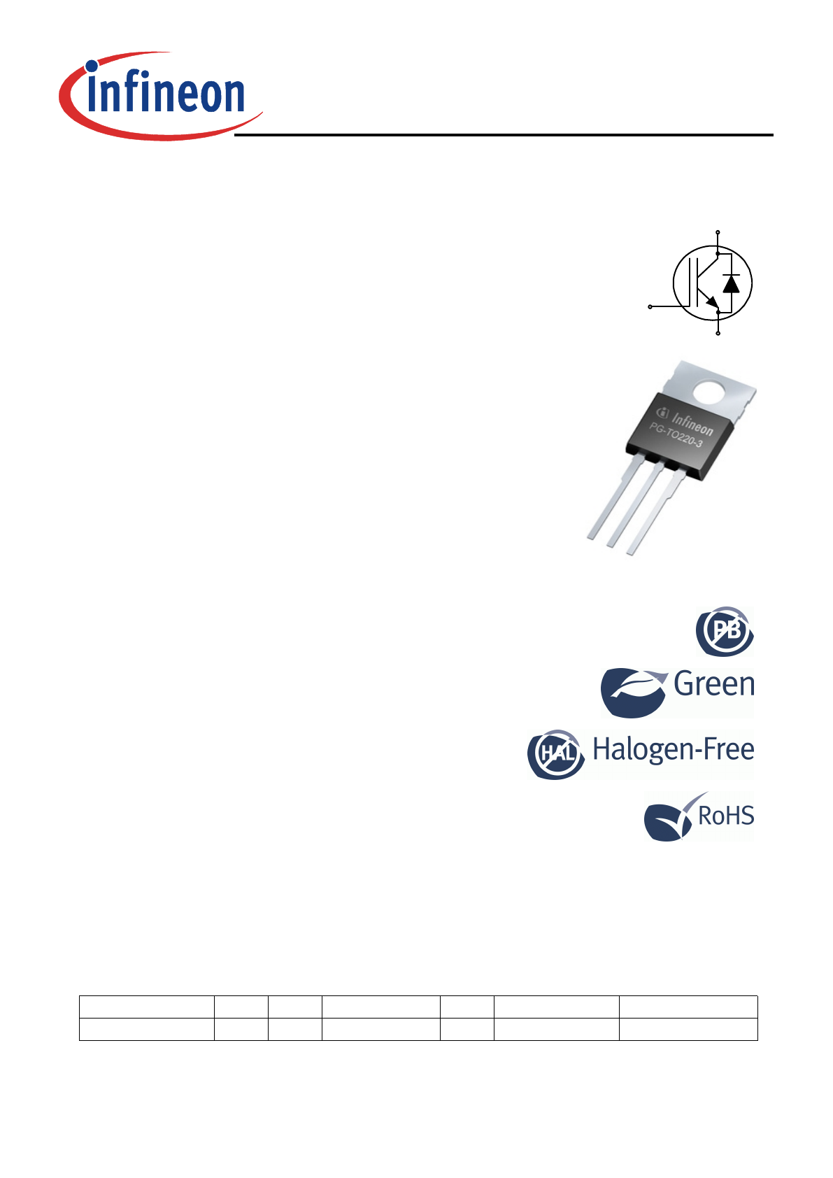
Figure 1.
Forwardbiassafeoperatingarea
(D=0,T
C
=25°C,T
vj
≤
175°C;V
GE
=15V.
RecommendeduseatV
GE
≥
7.5V)
V
CE
,COLLECTOR-EMITTERVOLTAGE[V]
I
C
,COLLECTORCURRENT[A]
1
10
100
1000
0.1
1
10
t
p
=1µs
10µs
50µs
100µs
200µs
500µs
DC
Figure 2.
Powerdissipationasafunctionofcase
temperature
(T
vj
≤
175°C)
T
C
,CASETEMPERATURE[°C]
P
tot
,POWERDISSIPATION[W]
25
50
75
100
125
150
175
0
10
20
30
40
50
60
70
80
Figure 3.
Collectorcurrentasafunctionofcase
temperature
(V
GE
≥
15V,T
vj
≤
175°C)
T
C
,CASETEMPERATURE[°C]
I
C
,COLLECTORCURRENT[A]
25
50
75
100
125
150
175
0
2
4
6
8
10
12
14
16
18
Figure 4.
Typicaloutputcharacteristic
(T
vj
=25°C)
V
CE
,COLLECTOR-EMITTERVOLTAGE[V]
I
C
,COLLECTORCURRENT[A]
0.0
0.5
1.0
1.5
2.0
2.5
3.0
3.5
4.0
0
3
6
9
12
15
18
21
24
V
GE
=20V
18V
12V
10V
8V
7V
6V
5V
9
IKP08N65F5
Highspeedswitchingseriesfifthgeneration
Rev.2.1,2015-05-05
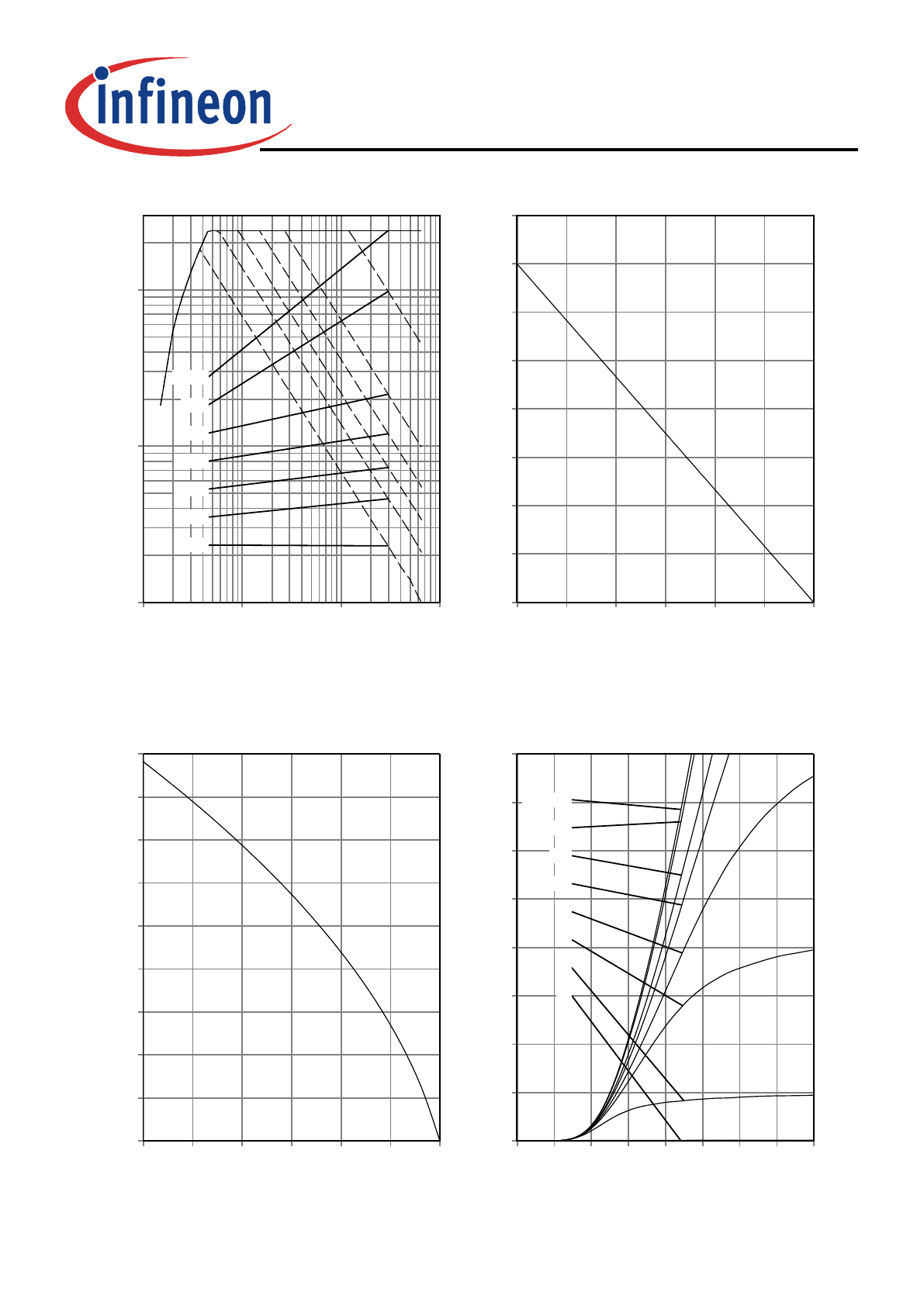
Figure 5.
Typicaloutputcharacteristic
(T
vj
=150°C)
V
CE
,COLLECTOR-EMITTERVOLTAGE[V]
I
C
,COLLECTORCURRENT[A]
0.0
0.5
1.0
1.5
2.0
2.5
3.0
3.5
4.0
0
3
6
9
12
15
18
21
24
V
GE
=20V
18V
12V
10V
8V
7V
6V
5V
Figure 6.
Typicaltransfercharacteristic
(V
CE
=20V)
V
GE
,GATE-EMITTERVOLTAGE[V]
I
C
,COLLECTORCURRENT[A]
4
5
6
7
8
9
0
3
6
9
12
15
18
21
24
T
j
=25°C
T
j
=150°C
Figure 7.
Typicalcollector-emittersaturationvoltageas
afunctionofjunctiontemperature
(V
GE
=15V)
T
vj
,JUNCTIONTEMPERATURE[°C]
V
CEsat
,COLLECTOR-EMITTERSATURATION[V]
0
25
50
75
100
125
150
175
0.75
1.00
1.25
1.50
1.75
2.00
I
C
=2A
I
C
=4A
I
C
=8A
Figure 8.
Typicalswitchingtimesasafunctionof
collectorcurrent
(inductiveload,T
vj
=150°C,V
CE
=400V,
V
GE
=15/0V,r
G
=48
Ω
,Dynamictestcircuitin
Figure E)
I
C
,COLLECTORCURRENT[A]
t,SWITCHINGTIMES[ns]
0
3
6
9
12
15
18
21
24
1
10
100
t
d(off)
t
f
t
d(on)
t
r
10
IKP08N65F5
Highspeedswitchingseriesfifthgeneration
Rev.2.1,2015-05-05
Figure 9.
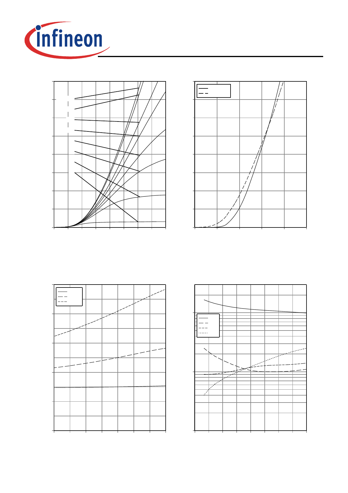
Typicalswitchingtimesasafunctionofgate
resistor
(inductiveload,T
vj
=150°C,V
CE
=400V,
V
GE
=15/0V,I
C
=4A,Dynamictestcircuitin
Figure E)
r
G
,GATERESISTOR[
Ω
]
t,SWITCHINGTIMES[ns]
5
15
25
35
45
55
65
75
85
1
10
100
t
d(off)
t
f
t
d(on)
t
r
Figure 10.
Typicalswitchingtimesasafunctionof
junctiontemperature
(inductiveload,V
CE
=400V,V
GE
=15/0V,
I
C
=4A,r
G
=48
Ω
,DynamictestcircuitinFigure
E)
T
vj
,JUNCTIONTEMPERATURE[°C]
t,SWITCHINGTIMES[ns]
25
50
75
100
125
150
175
1
10
100
t
d(off)
t
f
t
d(on)
t
r
Figure 11.
Gate-emitterthresholdvoltageasafunction
ofjunctiontemperature
(I
C
=0.08mA)
T
vj
,JUNCTIONTEMPERATURE[°C]
V
GE(th)
,GATE-EMITTERTHRESHOLDVOLTAGE[V]
0
25
50
75
100
125
150
175
1.0
1.5
2.0
2.5
3.0
3.5
4.0
4.5
5.0
5.5
typ.
min.
max.
Figure 12.
Typicalswitchingenergylossesasa
functionofcollectorcurrent
(inductiveload,T
vj
=150°C,V
CE
=400V,
V
GE
=15/0V,r
G
=48
Ω
,Dynamictestcircuitin
Figure E)
I
C
,COLLECTORCURRENT[A]
E
,SWITCHINGENERGYLOSSES[mJ]
0
3
6
9
12
15
18
21
24
0.0
0.1
0.2
0.3
0.4
0.5
0.6
0.7
0.8
E
off
E
on
E
ts