

ResonantSwitchingSeries
ReverseconductingIGBTwithmonolithicbodydiode
IHW30N110R3
Datasheet
IndustrialPowerControl

2
IHW30N110R3
ResonantSwitchingSeries
Rev.2.1,2015-01-26
ReverseconductingIGBTwithmonolithicbodydiode
Features:
•Powerfulmonolithicbodydiodewithlowforwardvoltage
designedforsoftcommutationonly
•Verytightparameterdistribution
•Highruggedness,temperaturestablebehavior
•LowV
CEsat
•Easyparallelswitchingcapabilityduetopositivetemperature
coefficientinV
CEsat
•LowEMI
•QualifiedaccordingtoJEDECfortargetapplications
•Pb-freeleadplating;RoHScompliant
•CompleteproductspectrumandPSpiceModels:
http://www.infineon.com/igbt/
Applications:
•Inductivecooking
•Inverterizedmicrowaveovens
•Resonantconverters
•Softswitchingapplications
G
C
E
G
C
E
KeyPerformanceandPackageParameters
Type
V
CE
I
C
V
CEsat
,T
vj
=25°C
T
vjmax
Marking
Package
IHW30N110R3
1100V
30A
1.55V
175°C
H30R1103
PG-TO247-3

3
IHW30N110R3
ResonantSwitchingSeries
Rev.2.1,2015-01-26
TableofContents
Description . . . . . . . . . . . . . . . . . . . . . . . . . . . . . . . . . . . . . . . . . . . . . . . . . . . . . . . . . . . . . . . . . . . . . . . . 2
Table of Contents . . . . . . . . . . . . . . . . . . . . . . . . . . . . . . . . . . . . . . . . . . . . . . . . . . . . . . . . . . . . . . . . . . . 3
Maximum Ratings . . . . . . . . . . . . . . . . . . . . . . . . . . . . . . . . . . . . . . . . . . . . . . . . . . . . . . . . . . . . . . . . . . . 4
Thermal Resistance . . . . . . . . . . . . . . . . . . . . . . . . . . . . . . . . . . . . . . . . . . . . . . . . . . . . . . . . . . . . . . . . . 4
Electrical Characteristics . . . . . . . . . . . . . . . . . . . . . . . . . . . . . . . . . . . . . . . . . . . . . . . . . . . . . . . . . . . . . . 5
Electrical Characteristics Diagrams . . . . . . . . . . . . . . . . . . . . . . . . . . . . . . . . . . . . . . . . . . . . . . . . . . . . . 7
Package Drawing . . . . . . . . . . . . . . . . . . . . . . . . . . . . . . . . . . . . . . . . . . . . . . . . . . . . . . . . . . . . . . . . . . .13
Testing Conditions . . . . . . . . . . . . . . . . . . . . . . . . . . . . . . . . . . . . . . . . . . . . . . . . . . . . . . . . . . . . . . . . . .14
Revision History . . . . . . . . . . . . . . . . . . . . . . . . . . . . . . . . . . . . . . . . . . . . . . . . . . . . . . . . . . . . . . . . . . . .15
Disclaimer . . . . . . . . . . . . . . . . . . . . . . . . . . . . . . . . . . . . . . . . . . . . . . . . . . . . . . . . . . . . . . . . . . . . . . . . .15

4
IHW30N110R3
ResonantSwitchingSeries
Rev.2.1,2015-01-26
MaximumRatings
Foroptimumlifetimeandreliability,Infineonrecommendsoperatingconditionsthatdonotexceed80%ofthemaximumratingsstatedinthisdatasheet.
Parameter
Symbol
Value
Unit
Collector-emitter voltage
V
CE
1100
V
DCcollectorcurrent,limitedbyT
vjmax
T
C
=25°C
T
C
=100°C
I
C
60.0
30.0
A
Pulsedcollectorcurrent,t
p
limitedbyT
vjmax
I
Cpuls
90.0
A
TurnoffsafeoperatingareaV
CE
≤
1100V,T
vj
≤
175°C
-
90.0
A
Diodeforwardcurrent,limitedbyT
vjmax
T
C
=25°C
T
C
=100°C
I
F
60.0
30.0
A
Diodepulsedcurrent,t
p
limitedbyT
vjmax
I
Fpuls
90.0
A
Gate-emitter voltage
TransientGate-emittervoltage(t
p
≤
10µs,D<0.010)
V
GE
±20
±25
V
PowerdissipationT
C
=25°C
PowerdissipationT
C
=100°C
P
tot
333.0
166.0
W
Operating junction temperature
T
vj
-40...+175
°C
Storage temperature
T
stg
-55...+175
°C
Soldering temperature,
wave soldering 1.6mm (0.063in.) from case for 10s
260
°C
Mounting torque, M3 screw
Maximum of mounting processes: 3
M
0.6
Nm
ThermalResistance
Parameter
Symbol Conditions
Max.Value
Unit
Characteristic
IGBT thermal resistance,
junction - case
R
th(j-c)
0.45
K/W
Diode thermal resistance,
junction - case
R
th(j-c)
0.45
K/W
Thermal resistance
junction - ambient
R
th(j-a)
40
K/W

5
IHW30N110R3
ResonantSwitchingSeries
Rev.2.1,2015-01-26
ElectricalCharacteristic,atT
vj
=25°C,unlessotherwisespecified
Value
min.
typ.
max.
Parameter
Symbol Conditions
Unit
StaticCharacteristic
Collector-emitter breakdown voltage
V
(BR)CES
V
GE
=0V,I
C
=0.50mA
1100
-
-
V
Collector-emitter saturation voltage
V
CEsat
V
GE
=15.0V,I
C
=30.0A
T
vj
=25°C
T
vj
=125°C
T
vj
=175°C
-
-
-
1.55
1.85
2.00
1.75
-
-
V
Diode forward voltage
V
F
V
GE
=0V,I
F
=30.0A
T
vj
=25°C
T
vj
=125°C
T
vj
=175°C
-
-
-
1.35
1.38
1.41
1.55
-
-
V
Gate-emitter threshold voltage
V
GE(th)
I
C
=0.70mA,V
CE
=V
GE
5.1
5.8
6.4
V
Zero gate voltage collector current
I
CES
V
CE
=1100V,V
GE
=0V
T
vj
=25°C
T
vj
=175°C
-
-
-
-
5.0
2500.0
µA
Gate-emitter leakage current
I
GES
V
CE
=0V,V
GE
=20V
-
-
100
nA
Transconductance
g
fs
V
CE
=20V,I
C
=30.0A
-
15.0
-
S
Integrated gate resistor
r
G
none
Ω
ElectricalCharacteristic,atT
vj
=25°C,unlessotherwisespecified
Value
min.
typ.
max.
Parameter
Symbol Conditions
Unit
DynamicCharacteristic
Input capacitance
C
ies
-
1460
-
Output capacitance
C
oes
-
55
-
Reverse transfer capacitance
C
res
-
45
-
V
CE
=25V,V
GE
=0V,f=1MHz
pF
Gate charge
Q
G
V
CC
=880V,I
C
=30.0A,
V
GE
=15V
-
180.0
-
nC
Internal emitter inductance
measured 5mm (0.197 in.) from
case
L
E
-
13.0
-
nH
SwitchingCharacteristic,InductiveLoad
Value
min.
typ.
max.
Parameter
Symbol Conditions
Unit
IGBTCharacteristic,atT
vj
=25°C
Turn-off delay time
t
d(off)
-
350
-
ns
Fall time
t
f
-
16
-
ns
Turn-off energy
E
off
-
1.15
-
mJ
T
vj
=25°C,
V
CC
=600V,I
C
=30.0A,
V
GE
=0.0/15.0V,
R
G(on)
=15.0
Ω
,R
G(off)
=15.0
Ω
,
L
σ
=80nH,C
σ
=39pF
L
σ
,C
σ
fromFig.E
Energy losses include “tail” and
diode reverse recovery.

6
IHW30N110R3
ResonantSwitchingSeries
Rev.2.1,2015-01-26
SwitchingCharacteristic,InductiveLoad
Value
min.
typ.
max.
Parameter
Symbol Conditions
Unit
IGBTCharacteristic,atT
vj
=175°C
Turn-off delay time
t
d(off)
-
410
-
ns
Fall time
t
f
-
60
-
ns
Turn-off energy
E
off
-
1.80
-
mJ
T
vj
=175°C,
V
CC
=600V,I
C
=30.0A,
V
GE
=0.0/15.0V,
R
G(on)
=15.0
Ω
,R
G(off)
=15.0
Ω
,
L
σ
=80nH,C
σ
=39pF
L
σ
,C
σ
fromFig.E
Energy losses include “tail” and
diode reverse recovery.
7
IHW30N110R3
ResonantSwitchingSeries
Rev.2.1,2015-01-26
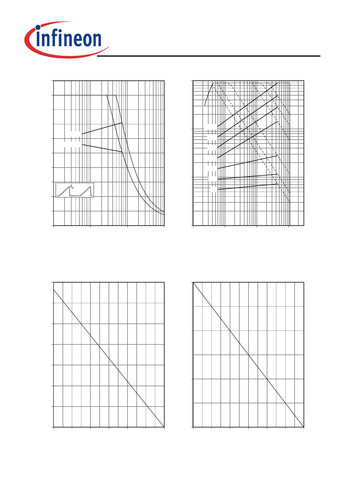
Figure 1.
Collectorcurrentasafunctionofswitching
frequency
(T
j
≤
175°C,D=0.5,V
CE
=600V,V
GE
=0/15V,
R
G
=15
Ω
)
f,SWITCHINGFREQUENCY[kHz]
I
C
,COLLECTORCURRENT[A]
1
10
100
1000
0
10
20
30
40
50
60
70
80
90
100
T
C
=80°
T
C
=110°
Figure 2.
Forwardbiassafeoperatingarea
(D=0,T
C
=25°C,T
j
≤
175°C;V
GE
=15V)
V
CE
,COLLECTOR-EMITTERVOLTAGE[V]
I
C
,COLLECTORCURRENT[A]
1
10
100
1000
0.1
1
10
100
t
p
=1µs
10µs
20µs
50µs
500µs
5ms
DC
Figure 3.
Powerdissipationasafunctionofcase
temperature
(T
j
≤
175°C)
T
C
,CASETEMPERATURE[°C]
P
tot
,POWERDISSIPATION[W]
25
50
75
100
125
150
175
0
50
100
150
200
250
300
350
Figure 4.
Collectorcurrentasafunctionofcase
temperature
(V
GE
≥
15V,T
j
≤
175°C)
T
C
,CASETEMPERATURE[°C]
I
C
,COLLECTORCURRENT[A]
25
50
75
100
125
150
175
0
20
40
60
8
IHW30N110R3
ResonantSwitchingSeries
Rev.2.1,2015-01-26
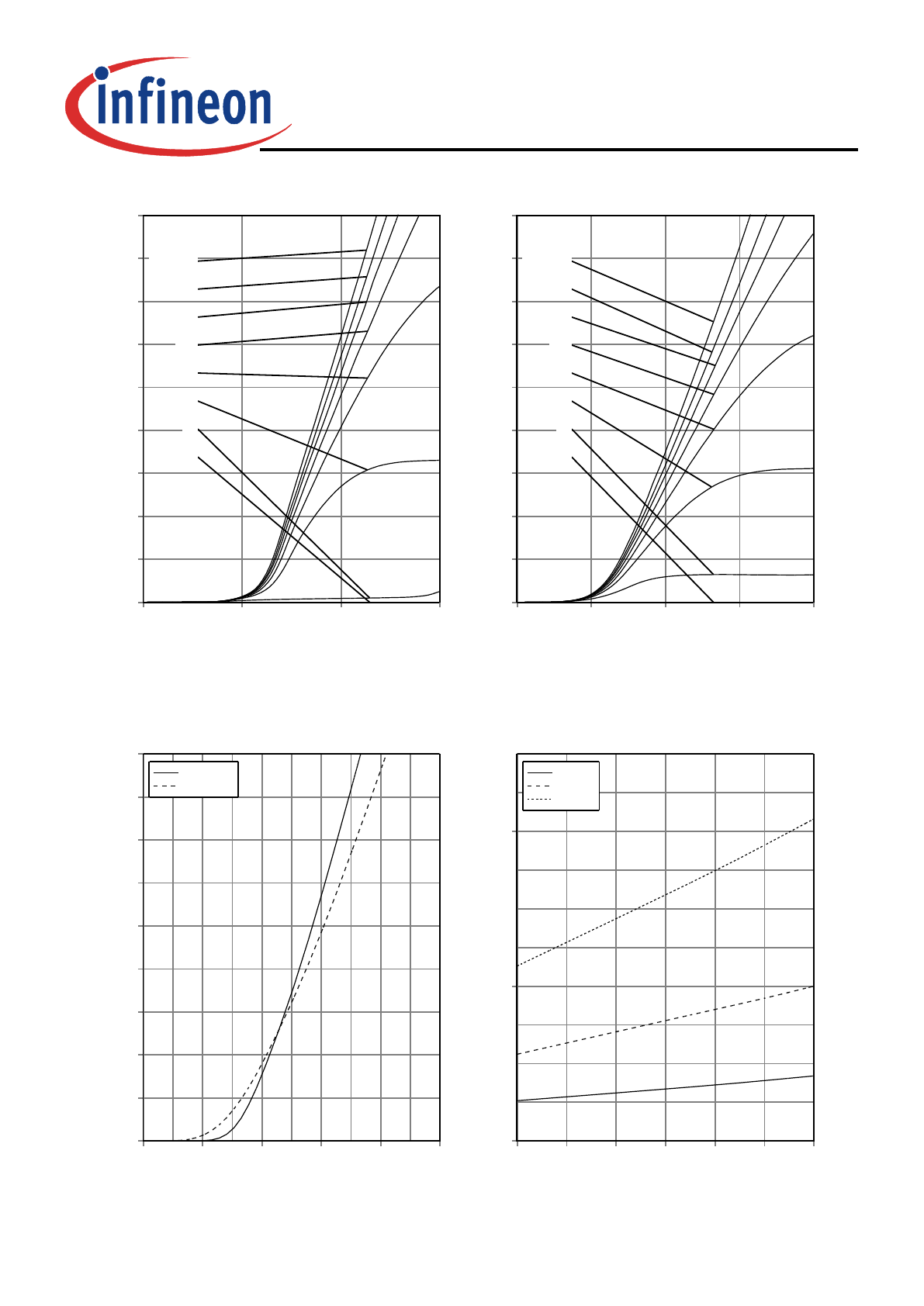
Figure 5.
Typicaloutputcharacteristic
(T
j
=25°C)
V
CE
,COLLECTOR-EMITTERVOLTAGE[V]
I
C
,COLLECTORCURRENT[A]
0
1
2
3
0
10
20
30
40
50
60
70
80
90
V
GE
=20V
17V
15V
13V
11V
9V
7V
5V
Figure 6.
Typicaloutputcharacteristic
(T
j
=175°C)
V
CE
,COLLECTOR-EMITTERVOLTAGE[V]
I
C
,COLLECTORCURRENT[A]
0
1
2
3
4
0
10
20
30
40
50
60
70
80
90
V
GE
=20V
17V
15V
13V
11V
9V
7V
5V
Figure 7.
Typicaltransfercharacteristic
(V
CE
=20V)
V
GE
,GATE-EMITTERVOLTAGE[V]
I
C
,COLLECTORCURRENT[A]
4
6
8
10
12
14
0
10
20
30
40
50
60
70
80
90
25°C
T
j
=175°C
Figure 8.
Typicalcollector-emittersaturationvoltageas
afunctionofjunctiontemperature
(V
GE
=15V)
T
j
,JUNCTIONTEMPERATURE[°C]
V
CE(sat)
,COLLECTOR-EMITTERSATURATION[V]
25
50
75
100
125
150
175
1
2
3
I
C
=15A
I
C
=30A
I
C
=60A
9
IHW30N110R3
ResonantSwitchingSeries
Rev.2.1,2015-01-26
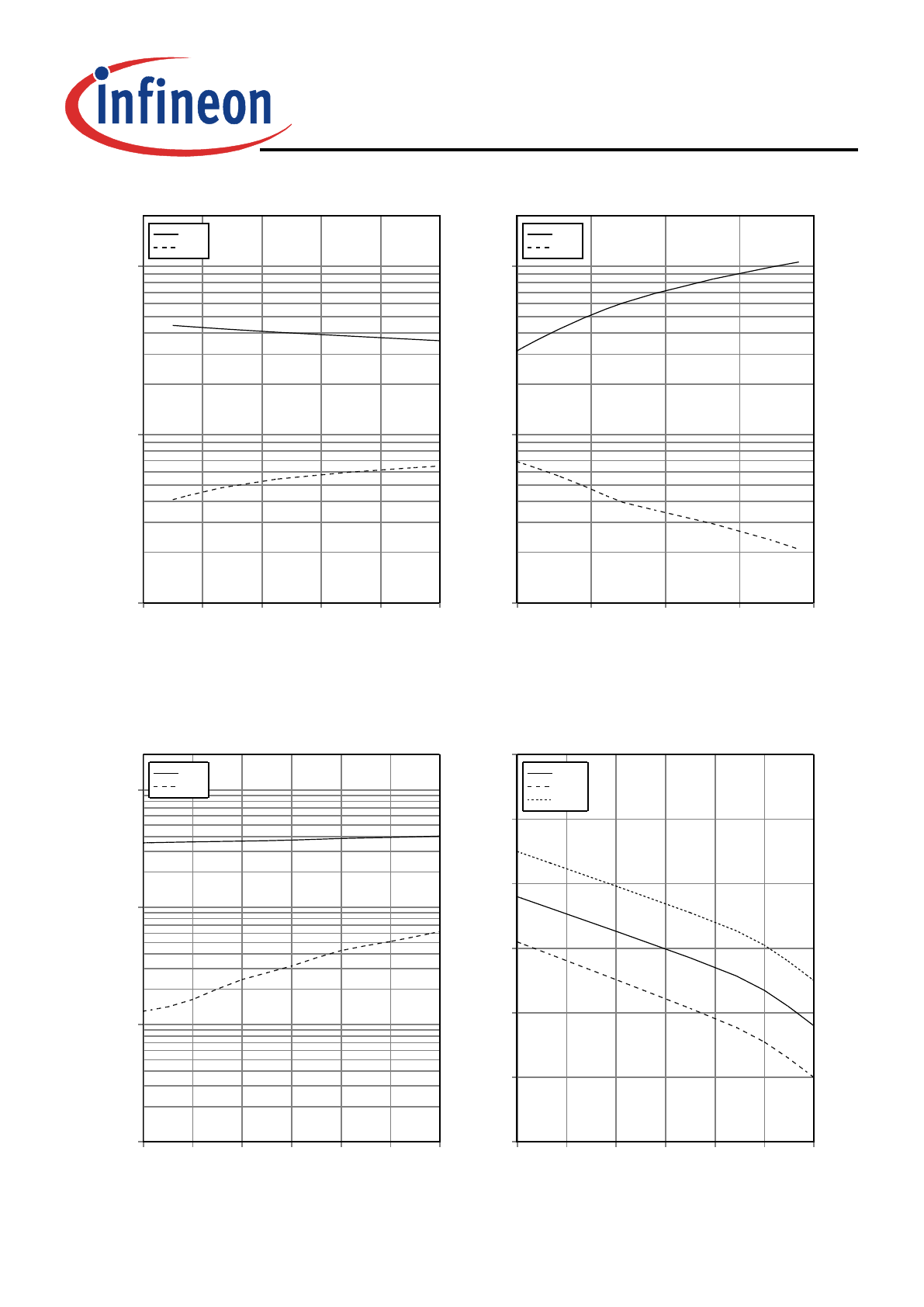
Figure 9.
Typicalswitchingtimesasafunctionof
collectorcurrent
(ind.load,T
j
=175°C,V
CE
=600V,V
GE
=0/15V,
R
G(on)
=15
Ω
,R
G(off)
=15
Ω
,testcircuitinFig.E)
I
C
,COLLECTORCURRENT[A]
t,SWITCHINGTIMES[ns]
10
20
30
40
50
60
10
100
1000
t
d(off)
t
f
Figure 10.
Typicalswitchingtimesasafunctionofgate
resistance
(ind.load,T
j
=175°C,V
CE
=600V,V
GE
=0/15V,
I
C
=30A,testcircuitinFig.E)
R
G
,GATERESISTANCE[
Ω
]
t,SWITCHINGTIMES[ns]
10
20
30
40
50
10
100
1000
t
d(off)
t
f
Figure 11.
Typicalswitchingtimesasafunctionof
junctiontemperature
(ind.load,V
CE
=600V,V
GE
=0/15V,I
C
=30A,
R
G(on)
=15
Ω
,R
G(off)
=15
Ω
,testcircuitinFig.E)
T
j
,JUNCTIONTEMPERATURE[°C]
t,SWITCHINGTIMES[ns]
25
50
75
100
125
150
175
1
10
100
1000
t
d(off)
t
f
Figure 12.
Gate-emitterthresholdvoltageasafunction
ofjunctiontemperature
(I
C
=0.7mA)
T
j
,JUNCTIONTEMPERATURE[°C]
V
GE(th)
,GATE-EMITTERTHRESHOLDVOLTAGE[V]
25
50
75
100
125
150
175
2
3
4
5
6
7
8
typ.
min.
max.

10
IHW30N110R3
ResonantSwitchingSeries
Rev.2.1,2015-01-26
Figure 13.
Typicalswitchingenergylossesasa
functionofcollectorcurrent
(ind.load,T
j
=175°C,V
CE
=600V,V
GE
=0/15V,
R
G(on)
=15
Ω
,R
G(off)
=15
Ω
,testcircuitinFig.E)
I
C
,COLLECTORCURRENT[A]
E
,SWITCHINGENERGYLOSSES[mJ]
0
15
30
45
60
0
1
2
3
4
E
off
Figure 14.
Typicalswitchingenergylossesasa
functionofgateresistance
(ind.load,T
j
=175°C,V
CE
=600V,V
GE
=0/15V,
test circuit in Fig. E)
R
G
,GATERESISTANCE[
Ω
]
E
,SWITCHINGENERGYLOSSES[mJ]
10
20
30
40
50
0
1
2
3
E
off
Figure 15.
Typicalswitchingenergylossesasa
functionofjunctiontemperature
(indload,V
CE
=600V,V
GE
=0/15V,I
C
=30A,
R
G(on)
=15
Ω
,R
G(off)
=15
Ω
,testcircuitinFig.E)
T
j
,JUNCTIONTEMPERATURE[°C]
E
,SWITCHINGENERGYLOSSES[mJ]
25
50
75
100
125
150
175
0
1
2
E
off
Figure 16.
Typicalswitchingenergylossesasa
functionofcollectoremittervoltage
(ind.load,T
j
=175°C,V
GE
=0/15V,I
C
=30A,
R
G(on)
=15
Ω
,R
G(off)
=15
Ω
,testcircuitinFig.E)
V
CE
,COLLECTOR-EMITTERVOLTAGE[V]
E
,SWITCHINGENERGYLOSSES[mJ]
300
400
500
600
700
800
900
1.2
1.4
1.6
1.8
2.0
2.2
E
off