

IGBT
HighspeedIGBTinTrenchandFieldstoptechnology
IGB30N60H3
600Vhighspeedswitchingseriesthirdgeneration
Datasheet
IndustrialPowerControl
2
IGB30N60H3
Highspeedswitchingseriesthirdgeneration
Rev.2.3,2014-03-11
HighspeedIGBTinTrenchandFieldstoptechnology
Features:
TRENCHSTOP
TM
technologyoffering
•verylowturn-offenergy
•lowV
CEsat
•lowEMI
•maximumjunctiontemperature175°C
•qualifiedaccordingtoJEDECfortargetapplications
•Pb-freeleadplating,halogen-freemouldcompound,RoHS
compliant
•completeproductspectrumandPSpiceModels:
http://www.infineon.com/igbt/
Applications:
•uninterruptiblepowersupplies
•weldingconverters
•converterswithhighswitchingfrequency
G
C
E
G
E
C
KeyPerformanceandPackageParameters
Type
V
CE
I
C
V
CEsat
,T
vj
=25°C
T
vjmax
Marking
Package
IGB30N60H3
600V
30A
1.95V
175°C
G30H603
PG-TO263-3

3
IGB30N60H3
Highspeedswitchingseriesthirdgeneration
Rev.2.3,2014-03-11
TableofContents
Description . . . . . . . . . . . . . . . . . . . . . . . . . . . . . . . . . . . . . . . . . . . . . . . . . . . . . . . . . . . . . . . . . . . . . . . . 2
Table of Contents . . . . . . . . . . . . . . . . . . . . . . . . . . . . . . . . . . . . . . . . . . . . . . . . . . . . . . . . . . . . . . . . . . . 3
Maximum ratings . . . . . . . . . . . . . . . . . . . . . . . . . . . . . . . . . . . . . . . . . . . . . . . . . . . . . . . . . . . . . . . . . . . . 4
Thermal Resistance . . . . . . . . . . . . . . . . . . . . . . . . . . . . . . . . . . . . . . . . . . . . . . . . . . . . . . . . . . . . . . . . . 4
Electrical Characteristics . . . . . . . . . . . . . . . . . . . . . . . . . . . . . . . . . . . . . . . . . . . . . . . . . . . . . . . . . . . . . . 4
Electrical Characteristics diagrams . . . . . . . . . . . . . . . . . . . . . . . . . . . . . . . . . . . . . . . . . . . . . . . . . . . . . . 6
Package Drawing . . . . . . . . . . . . . . . . . . . . . . . . . . . . . . . . . . . . . . . . . . . . . . . . . . . . . . . . . . . . . . . . . . .12
Testing Conditions . . . . . . . . . . . . . . . . . . . . . . . . . . . . . . . . . . . . . . . . . . . . . . . . . . . . . . . . . . . . . . . . . .13
Revision History . . . . . . . . . . . . . . . . . . . . . . . . . . . . . . . . . . . . . . . . . . . . . . . . . . . . . . . . . . . . . . . . . . . .14
Disclaimer . . . . . . . . . . . . . . . . . . . . . . . . . . . . . . . . . . . . . . . . . . . . . . . . . . . . . . . . . . . . . . . . . . . . . . . . .14

4
IGB30N60H3
Highspeedswitchingseriesthirdgeneration
Rev.2.3,2014-03-11
Maximumratings
Parameter
Symbol
Value
Unit
Collector-emittervoltage,T
vj
≥
25°C
V
CE
600
V
DCcollectorcurrent,limitedbyT
vjmax
T
C
=25°C
T
C
=100°C
I
C
60.0
30.0
A
Pulsedcollectorcurrent,t
p
limitedbyT
vjmax
I
Cpuls
120.0
A
Turn off safe operating area
V
CE
≤
600V,T
vj
≤
175°C,t
p
=1µs
-
120.0
A
Gate-emitter voltage
V
GE
±20
V
Short circuit withstand time
V
GE
=15.0V,V
CC
≤
400V
Allowed number of short circuits < 1000
Time between short circuits:
≥
1.0s
T
vj
=150°C
t
SC
5
µs
PowerdissipationT
C
=25°C
PowerdissipationT
C
=100°C
P
tot
187.0
94.0
W
Operating junction temperature
T
vj
-40...+175
°C
Storage temperature
T
stg
-55...+150
°C
Soldering temperature,
reflow soldering (MSL1 according to JEDEC J-STA-020)
260
°C
ThermalResistance
Parameter
Symbol Conditions
Max.Value
Unit
Characteristic
IGBT thermal resistance,
junction - case
R
th(j-c)
0.80
K/W
Thermal resistance, min. footprint
junction - ambient
R
th(j-a)
65
K/W
Thermal resistance, 6cm² Cu on
PCB
junction - ambient
R
th(j-a)
40
K/W
ElectricalCharacteristic,atT
vj
=25°C,unlessotherwisespecified
Value
min.
typ.
max.
Parameter
Symbol Conditions
Unit
StaticCharacteristic
Collector-emitter breakdown voltage
V
(BR)CES
V
GE
=0V,I
C
=2.00mA
600
-
-
V
Collector-emitter saturation voltage
V
CEsat
V
GE
=15.0V,I
C
=30.0A
T
vj
=25°C
T
vj
=125°C
T
vj
=175°C
-
-
-
1.95
2.30
2.50
2.40
-
-
V
Gate-emitter threshold voltage
V
GE(th)
I
C
=0.43mA,V
CE
=V
GE
4.1
5.1
5.7
V
Zero gate voltage collector current
I
CES
V
CE
=600V,V
GE
=0V
T
vj
=25°C
T
vj
=175°C
-
-
-
-
40.0
2000.0
µA
Gate-emitter leakage current
I
GES
V
CE
=0V,V
GE
=20V
-
-
100
nA
Transconductance
g
fs
V
CE
=20V,I
C
=30.0A
-
16.0
-
S
5
IGB30N60H3
Highspeedswitchingseriesthirdgeneration
Rev.2.3,2014-03-11
ElectricalCharacteristic,atT
vj
=25°C,unlessotherwisespecified
Value
min.
typ.
max.
Parameter
Symbol Conditions
Unit
DynamicCharacteristic
Input capacitance
C
ies
-
1630
-
Output capacitance
C
oes
-
107
-
Reverse transfer capacitance
C
res
-
50
-
V
CE
=25V,V
GE
=0V,f=1MHz
pF
Gate charge
Q
G
V
CC
=480V,I
C
=30.0A,
V
GE
=15V
-
165.0
-
nC
Short circuit collector current
Max. 1000 short circuits
Time between short circuits:
≥
1.0s
I
C(SC)
V
GE
=15.0V,V
CC
≤
400V,
t
SC
≤
5µs
T
vj
=150°C
-
160
-
A
SwitchingCharacteristic,InductiveLoad
Value
min.
typ.
max.
Parameter
Symbol Conditions
Unit
IGBTCharacteristic,atT
vj
=25°C
Turn-on delay time
t
d(on)
-
18
-
ns
Rise time
t
r
-
22
-
ns
Turn-off delay time
t
d(off)
-
207
-
ns
Fall time
t
f
-
22
-
ns
Turn-on energy
E
on
-
0.73
-
mJ
Turn-off energy
E
off
-
0.44
-
mJ
Total switching energy
E
ts
-
1.17
-
mJ
T
vj
=25°C,
V
CC
=400V,I
C
=30.0A,
V
GE
=0.0/15.0V,
r
G
=10.5
Ω
,L
σ
=95nH,
C
σ
=67pF
L
σ
,C
σ
fromFig.E
Energy losses include “tail” and
diode (IKW30N60H3) reverse
recovery.
SwitchingCharacteristic,InductiveLoad
Value
min.
typ.
max.
Parameter
Symbol Conditions
Unit
IGBTCharacteristic,atT
vj
=175°C
Turn-on delay time
t
d(on)
-
18
-
ns
Rise time
t
r
-
22
-
ns
Turn-off delay time
t
d(off)
-
239
-
ns
Fall time
t
f
-
23
-
ns
Turn-on energy
E
on
-
0.95
-
mJ
Turn-off energy
E
off
-
0.60
-
mJ
Total switching energy
E
ts
-
1.55
-
mJ
T
vj
=175°C,
V
CC
=400V,I
C
=30.0A,
V
GE
=0.0/15.0V,
r
G
=10.5
Ω
,L
σ
=95nH,
C
σ
=67pF
L
σ
,C
σ
fromFig.E
Energy losses include “tail” and
diode (IKW30N60H3) reverse
recovery.
6
IGB30N60H3
Highspeedswitchingseriesthirdgeneration
Rev.2.3,2014-03-11
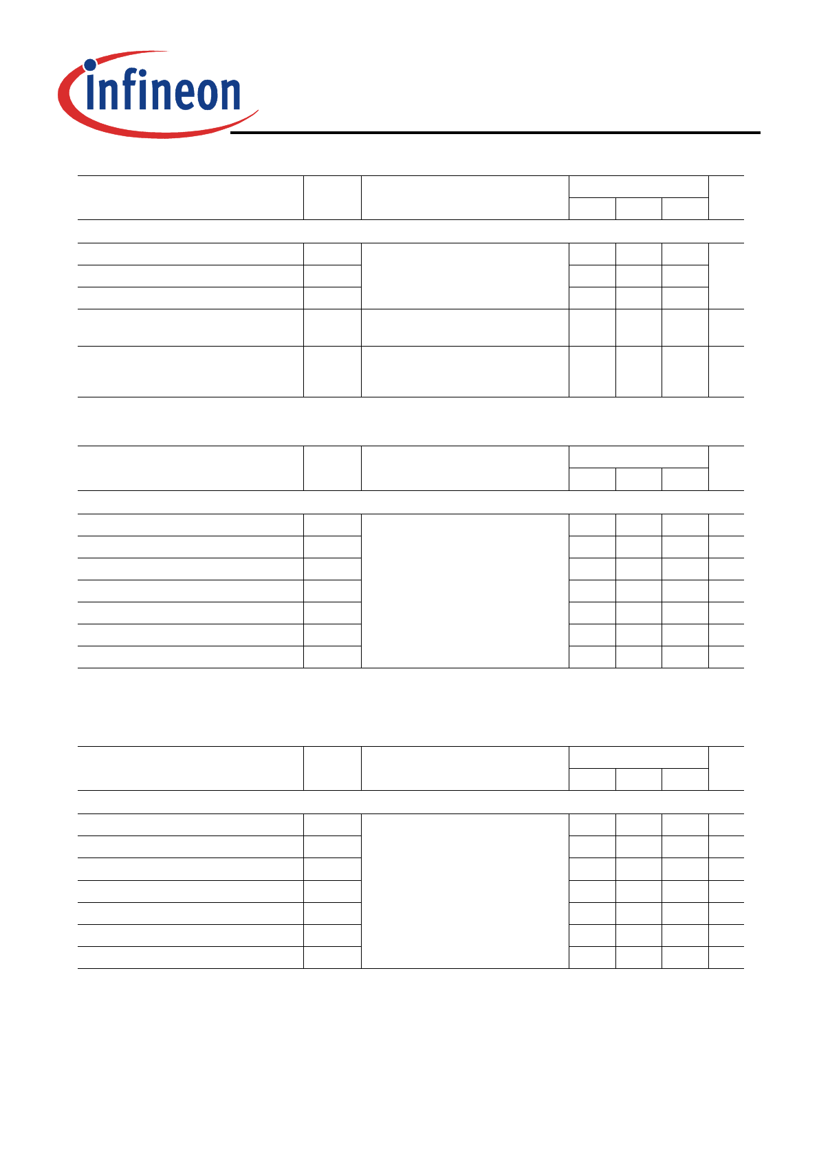
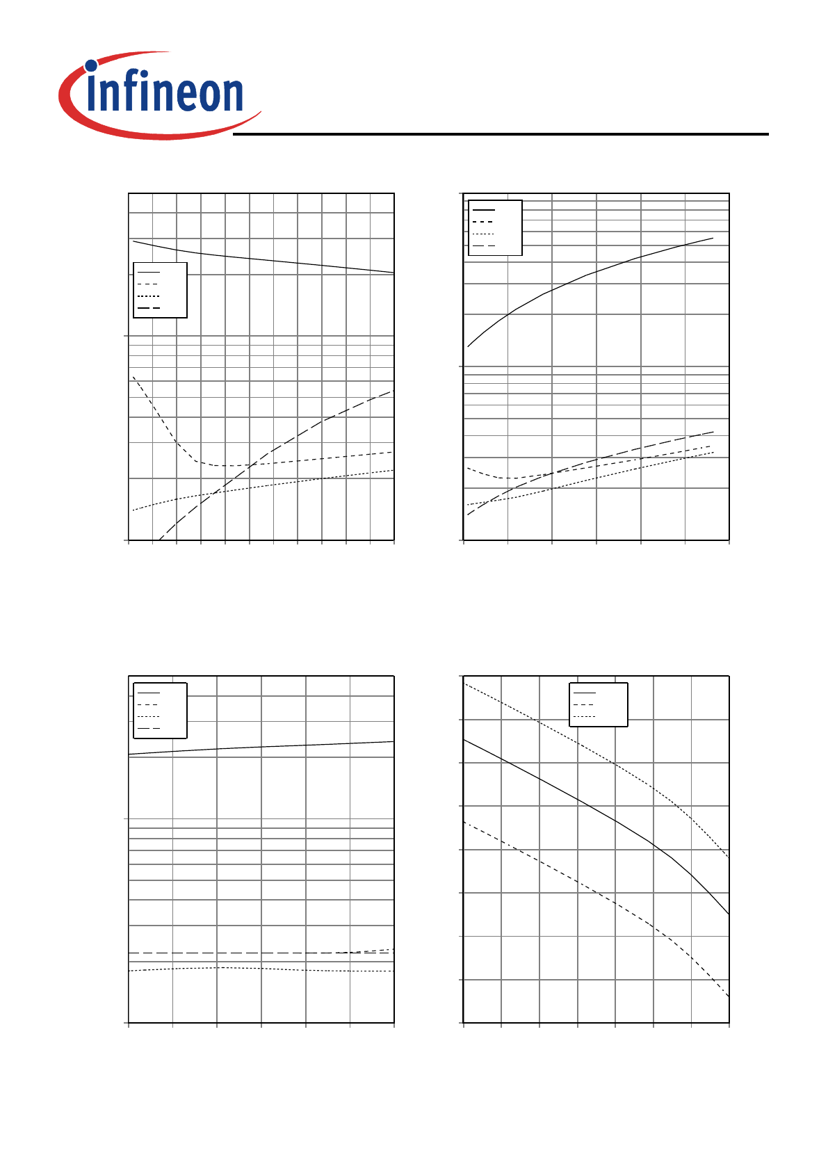
Figure 1.
Collectorcurrentasafunctionofswitching
frequency
(T
j
≤
175°C,D=0.5,V
CE
=400V,V
GE
=15/0V,
r
G
=10,5
Ω
)
f,SWITCHINGFREQUENCY[kHz]
I
C
,COLLECTORCURRENT[A]
1
10
100
1000
0
10
20
30
40
50
60
70
80
T
C
=80°
T
C
=110°
T
C
=80°
T
C
=110°
Figure 2.
Forwardbiassafeoperatingarea
(D=0,T
C
=25°C,T
j
≤
175°C;V
GE
=15V)
V
CE
,COLLECTOR-EMITTERVOLTAGE[V]
I
C
,COLLECTORCURRENT[A]
1
10
100
1000
0.1
1
10
100
t
p
=1µs
10µs
50µs
100µs
200µs
500µs
DC
Figure 3.
Powerdissipationasafunctionofcase
temperature
(T
j
≤
175°C)
T
C
,CASETEMPERATURE[°C]
P
tot
,POWERDISSIPATION[W]
25
50
75
100
125
150
175
0
25
50
75
100
125
150
175
200
Figure 4.
Collectorcurrentasafunctionofcase
temperature
(V
GE
≥
15V,T
j
≤
175°C)
T
C
,CASETEMPERATURE[°C]
I
C
,COLLECTORCURRENT[A]
25
50
75
100
125
150
175
0
10
20
30
40
50
60
7
IGB30N60H3
Highspeedswitchingseriesthirdgeneration
Rev.2.3,2014-03-11
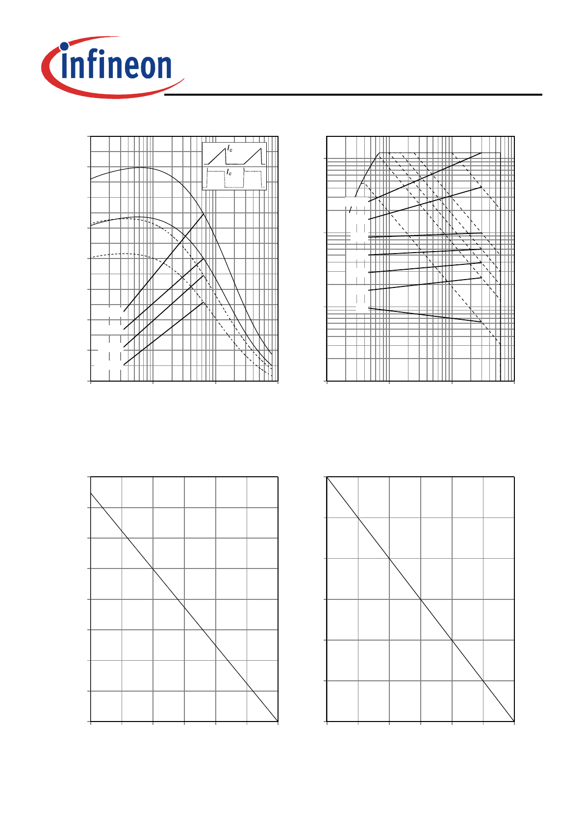
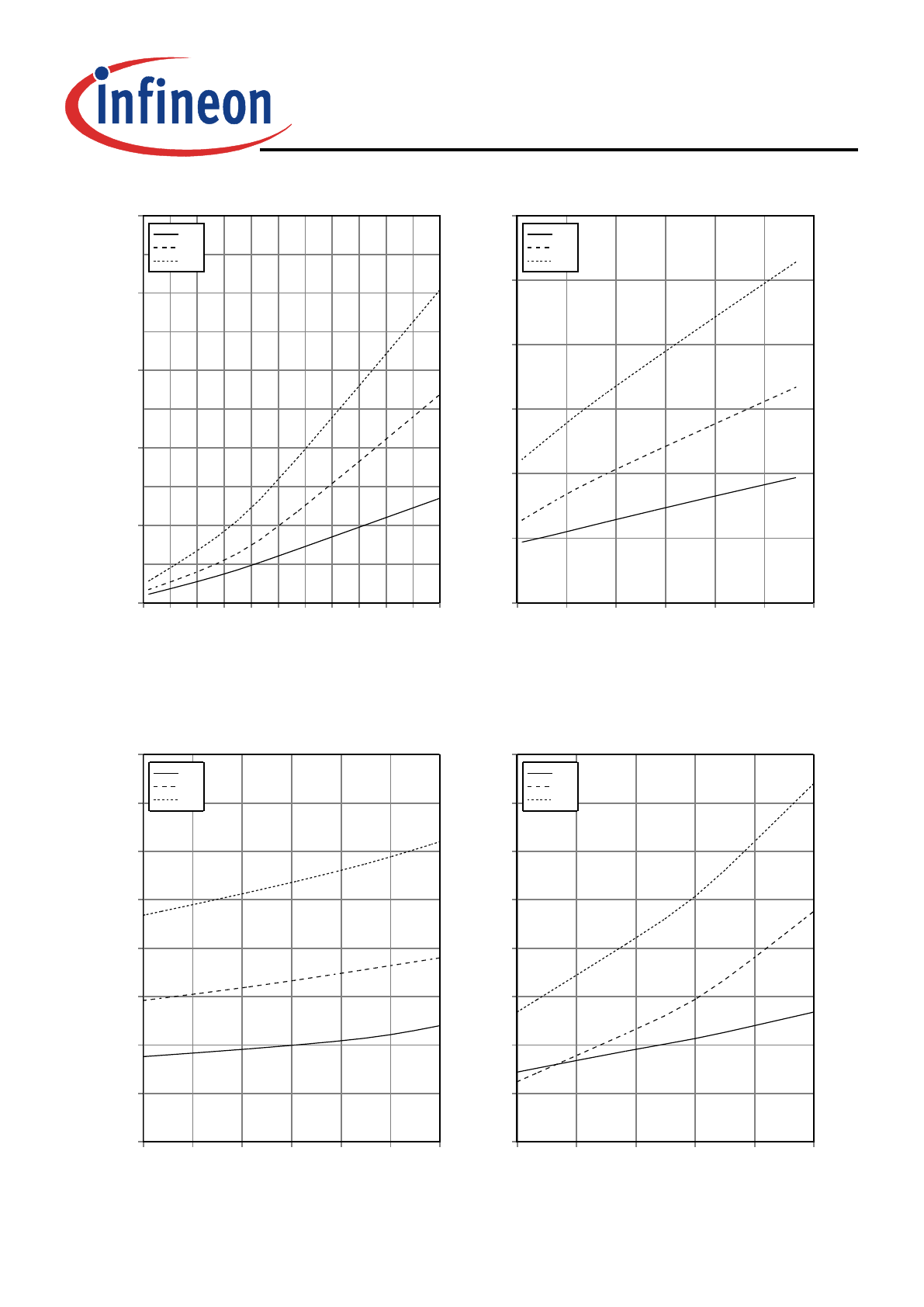
Figure 5.
Typicaloutputcharacteristic
(T
j
=25°C)
V
CE
,COLLECTOR-EMITTERVOLTAGE[V]
I
C
,COLLECTORCURRENT[A]
0
1
2
3
4
5
6
0
20
40
60
80
100
120
V
GE
=20V
17V
15V
13V
11V
9V
7V
5V
Figure 6.
Typicaloutputcharacteristic
(T
j
=175°C)
V
CE
,COLLECTOR-EMITTERVOLTAGE[V]
I
C
,COLLECTORCURRENT[A]
0
1
2
3
4
5
6
7
8
0
20
40
60
80
100
120
V
GE
=20V
17V
15V
13V
11V
9V
7V
5V
Figure 7.
Typicaltransfercharacteristic
(V
CE
=20V)
V
GE
,GATE-EMITTERVOLTAGE[V]
I
C
,COLLECTORCURRENT[A]
5
6
7
8
9
10
11
12
0
10
20
30
40
50
60
70
80
90
100
T
j
=25°C
T
j
=175°C
Figure 8.
Typicalcollector-emittersaturationvoltageas
afunctionofjunctiontemperature
(V
GE
=15V)
T
j
,JUNCTIONTEMPERATURE[°C]
V
CE(sat)
,COLLECTOR-EMITTERSATURATION[V]
0
25
50
75
100
125
150
175
1.0
1.5
2.0
2.5
3.0
3.5
4.0
I
C
=15A
I
C
=30A
I
C
=60A
8
IGB30N60H3
Highspeedswitchingseriesthirdgeneration
Rev.2.3,2014-03-11
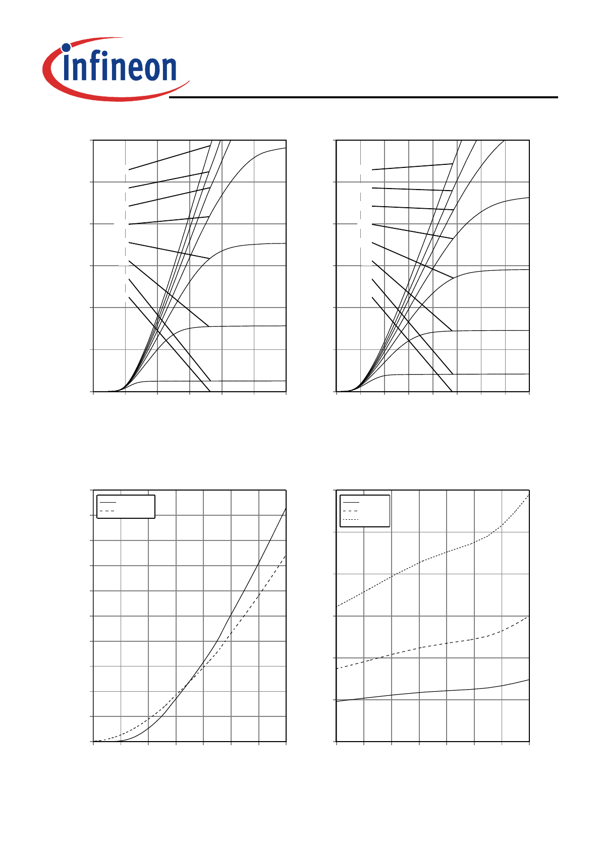
Figure 9.
Typicalswitchingtimesasafunctionof
collectorcurrent
(ind.load,T
j
=175°C,V
CE
=400V,V
GE
=15/0V,
r
G
=10,5
Ω
,testcircuitinFig.E)
I
C
,COLLECTORCURRENT[A]
t,SWITCHINGTIMES[ns]
5
10 15 20 25 30 35 40 45 50 55 60
10
100
t
d(off)
t
f
t
d(on)
t
r
Figure 10.
Typicalswitchingtimesasafunctionofgate
resistor
(ind.load,T
j
=175°C,V
CE
=400V,V
GE
=15/0V,
I
C
=30A,testcircuitinFig.E)
r
G
,GATERESISTOR[
Ω
]
t,SWITCHINGTIMES[ns]
3
8
13
18
23
28
33
10
100
1000
t
d(off)
t
f
t
d(on)
t
r
Figure 11.
Typicalswitchingtimesasafunctionof
junctiontemperature
(ind.load,V
CE
=400V,V
GE
=15/0V,I
C
=30A,
r
G
=10,5
Ω
,testcircuitinFig.E)
T
j
,JUNCTIONTEMPERATURE[°C]
t,SWITCHINGTIMES[ns]
25
50
75
100
125
150
175
10
100
t
d(off)
t
f
t
d(on)
t
r
Figure 12.
Gate-emitterthresholdvoltageasafunction
ofjunctiontemperature
(I
C
=0.43mA)
T
j
,JUNCTIONTEMPERATURE[°C]
V
GE(th)
,GATE-EMITTERTHRESHOLDVOLTAGE[V]
0
25
50
75
100
125
150
175
2.0
2.5
3.0
3.5
4.0
4.5
5.0
5.5
6.0
typ.
min.
max.
9
IGB30N60H3
Highspeedswitchingseriesthirdgeneration
Rev.2.3,2014-03-11
Figure 13.
Typicalswitchingenergylossesasa
functionofcollectorcurrent
(ind.load,T
j
=175°C,V
CE
=400V,V
GE
=15/0V,
r
G
=10,5
Ω
,testcircuitinFig.E)
I
C
,COLLECTORCURRENT[A]
E
,SWITCHINGENERGYLOSSES[mJ]
5
10 15 20 25 30 35 40 45 50 55 60
0
1
2
3
4
5
E
off
E
on
E
ts
Figure 14.
Typicalswitchingenergylossesasa
functionofgateresistor
(ind.load,T
j
=175°C,V
CE
=400V,V
GE
=15/0V,
I
C
=30A,testcircuitinFig.E)
r
G
,GATERESISTOR[
Ω
]
E
,SWITCHINGENERGYLOSSES[mJ]
3
8
13
18
23
28
33
0.0
0.5
1.0
1.5
2.0
2.5
3.0
E
off
E
on
E
ts
Figure 15.
Typicalswitchingenergylossesasa
functionofjunctiontemperature
(indload,V
CE
=400V,V
GE
=15/0V,I
C
=30A,
r
G
=10,5
Ω
,testcircuitinFig.E)
T
j
,JUNCTIONTEMPERATURE[°C]
E
,SWITCHINGENERGYLOSSES[mJ]
25
50
75
100
125
150
175
0.00
0.25
0.50
0.75
1.00
1.25
1.50
1.75
2.00
E
off
E
on
E
ts
Figure 16.
Typicalswitchingenergylossesasa
functionofcollectoremittervoltage
(ind.load,T
j
=175°C,V
GE
=15/0V,I
C
=30A,
r
G
=10,5
Ω
,testcircuitinFig.E)
V
CE
,COLLECTOR-EMITTERVOLTAGE[V]
E
,SWITCHINGENERGYLOSSES[mJ]
200
250
300
350
400
450
0.00
0.25
0.50
0.75
1.00
1.25
1.50
1.75
2.00
E
off
E
on
E
ts
10
IGB30N60H3
Highspeedswitchingseriesthirdgeneration
Rev.2.3,2014-03-11
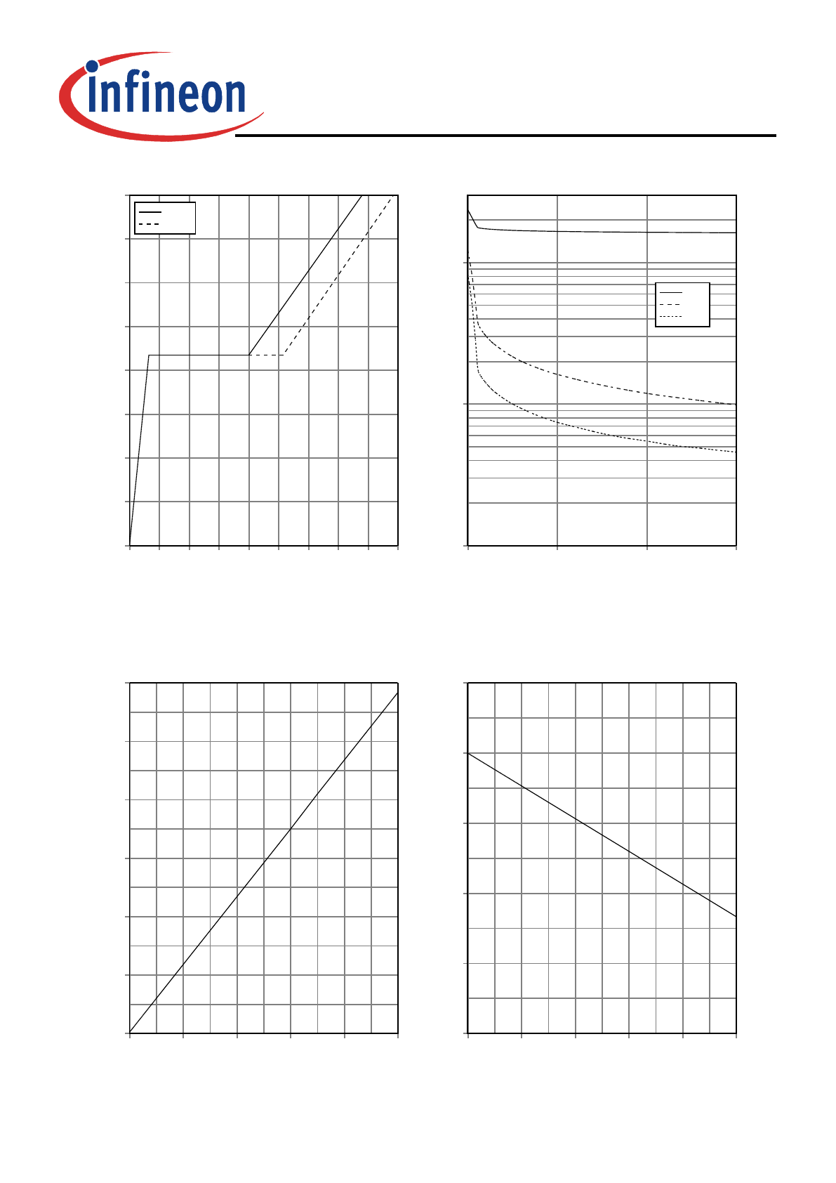
Figure 17.
Typicalgatecharge
(I
C
=30A)
Q
GE
,GATECHARGE[nC]
V
GE
,GATE-EMITTERVOLTAGE[V]
0
20
40
60
80
100 120 140 160 180
0
2
4
6
8
10
12
14
16
120V
480V
Figure 18.
Typicalcapacitanceasafunctionof
collector-emittervoltage
(V
GE
=0V,f=1MHz)
V
CE
,COLLECTOR-EMITTERVOLTAGE[V]
C
,CAPACITANCE[pF]
0
10
20
30
10
100
1000
C
ies
C
oes
C
res
Figure 19.
Typicalshortcircuitcollectorcurrentasa
functionofgate-emittervoltage
(V
CE
≤
400V,startatT
j
=25°C)
V
GE
,GATE-EMITTERVOLTAGE[V]
I
C(SC)
,SHORTCIRCUITCOLLECTORCURRENT[A]
10
12
14
16
18
20
80
130
180
230
280
330
380
Figure 20.
Shortcircuitwithstandtimeasafunctionof
gate-emittervoltage
(V
CE
≤
400V,startatT
j
≤
150°C)
V
GE
,GATE-EMITTERVOLTAGE[V]
t
SC
,SHORTCIRCUITWITHSTANDTIME[µs]
10
11
12
13
14
15
0
3
6
9
12
15