

CoolSET
®
-F3R
I C E 3 R B R 4 7 6 5 J Z
O f f - L i n e S M P S C u r r e n t M o d e
C o n t r o l l e r w i t h i n t e g r a t e d 6 5 0 V
C o o l M O S
®
a n d S t a r t u p c e l l
( f r e q u e n c y j i t t e r M o d e ) i n D I P - 7
N e v e r s t o p t h i n k i n g .
P o w e r M a n a g e m e n t & S u p p l y
V e r s i o n 2 . 0 , 7 J u n 2 0 1 3

Edition 2013-6-7
Published by
Infineon Technologies AG,
81726 Munich, Germany,
©
2013 Infineon Technologies AG.
All Rights Reserved.
Legal disclaimer
The information given in this document shall in no event be regarded as a guarantee of conditions or
characteristics. With respect to any examples or hints given herein, any typical values stated herein and/or any
information regarding the application of the device, Infineon Technologies hereby disclaims any and all warranties
and liabilities of any kind, including without limitation, warranties of non-infringement of intellectual property rights
of any third party.
Information
For further information on technology, delivery terms and conditions and prices, please contact your nearest
Infineon Technologies Office (www.infineon.com).
Warnings
Due to technical requirements, components may contain dangerous substances. For information on the types in
question, please contact your nearest Infineon Technologies Office.
Infineon Technologies Components may be used in life-support devices or systems only with the express written
approval of Infineon Technologies, if a failure of such components can reasonably be expected to cause the failure
of that life-support device or system or to affect the safety or effectiveness of that device or system. Life support
devices or systems are intended to be implanted in the human body or to support and/or maintain and sustain
and/or protect human life. If they fail, it is reasonable to assume that the health of the user or other persons may
be endangered.
For questions on technology, delivery and prices please contact the Infineon Technologies Offices in Germany or
the Infineon Technologies Companies and Representatives worldwide: see our webpage at http://
www.infineon.com
CoolMOS
®
, CoolSET
®
are trademarks of Infineon Technologies AG.
ICE3RBR4765JZ
Revision History:
2013-6-7
Version 2.0
Previous Version: 0.0
Page
Subjects (major changes since last revision)
3
add applications
Type
Package
Marking
V
DS
F
OSC
R
DSon
1)
1)
typ @ T
j
=25°C
230VAC ±15%
2)
2)
Calculated maximum input power rating at T
a
=50°C, T
i
=125°C and without copper area as heat sink. Refer to input power curve for other T
a
.
85-265 VAC
2)
ICE3RBR4765JZ
PG-DIP-7
3RBR4765JZ
650V
65kHz
4.70
26W
18W
ICE3RBR4765JZ
Version 2.0
3
7 Jun 2013
Off-Line SMPS Current Mode Controller with
integrated 650V CoolMOS
®
and Startup cell
(frequency jitter Mode) in DIP-7
P-DIP-7-1
PG-DIP-7
Description
ICE3RBR4765JZ (ICE3RBRxx65JZ series) is modified
from ICE3BRxx65J in DIP-7 package. It has more robust
design and can work to -40°C. The outstanding
performance includes BiCMOS technology, active burst
mode, built-in frequency jitter, soft gate driving,
propagation delay compensation, built-in soft start time,
built-in blanking time and extendable blanking time for
over load protection, external auto-restart enable feature,
etc.
Applications
•
Adapter/Charger
•
Blue Ray/DVD player, Set-top Box, Digital Photo
Frame
•
Auxiliary power supply for Server, PC, Printer, TV,
Home theater/Audio System, White Goods, etc
Product Highlights
•
Active Burst Mode to reach the lowest Standby Power
Requirements < 50mW
•
Auto Restart protection for overload, overtemperature, overvoltage
•
External auto-restart enable function
•
Built-in soft start and blanking window
•
Extendable blanking Window for high load jumps
•
Built-in frequency jitter and soft driving for low EMI
•
Low Operating temperature down to -40°C
•
Green Mould Compound
•
Pb-free lead plating; RoHS compliant
Features
•
650V avalanche rugged CoolMOS
®
with built-in
Startup Cell
•
Active Burst Mode for lowest Standby Power
•
Fast load jump response in Active Burst Mode
•
65kHz internally fixed switching frequency
•
Auto Restart Protection Mode for Overload, Open
Loop, VCC Undervoltage, Overtemperature &
Overvoltage
•
Built-in Soft Start
•
Built-in blanking window with extendable blanking
time for short duration high current
•
External auto-restart enable pin
•
Max Duty Cycle 75%
•
Overall tolerance of Current Limiting < ±5%
•
Internal PWM Leading Edge Blanking
•
BiCMOS technology provide wide VCC range
•
Built-in Frequency jitter and soft driving for low EMI
C
VCC
C
Bulk
Converter
DC Output
+
Snubber
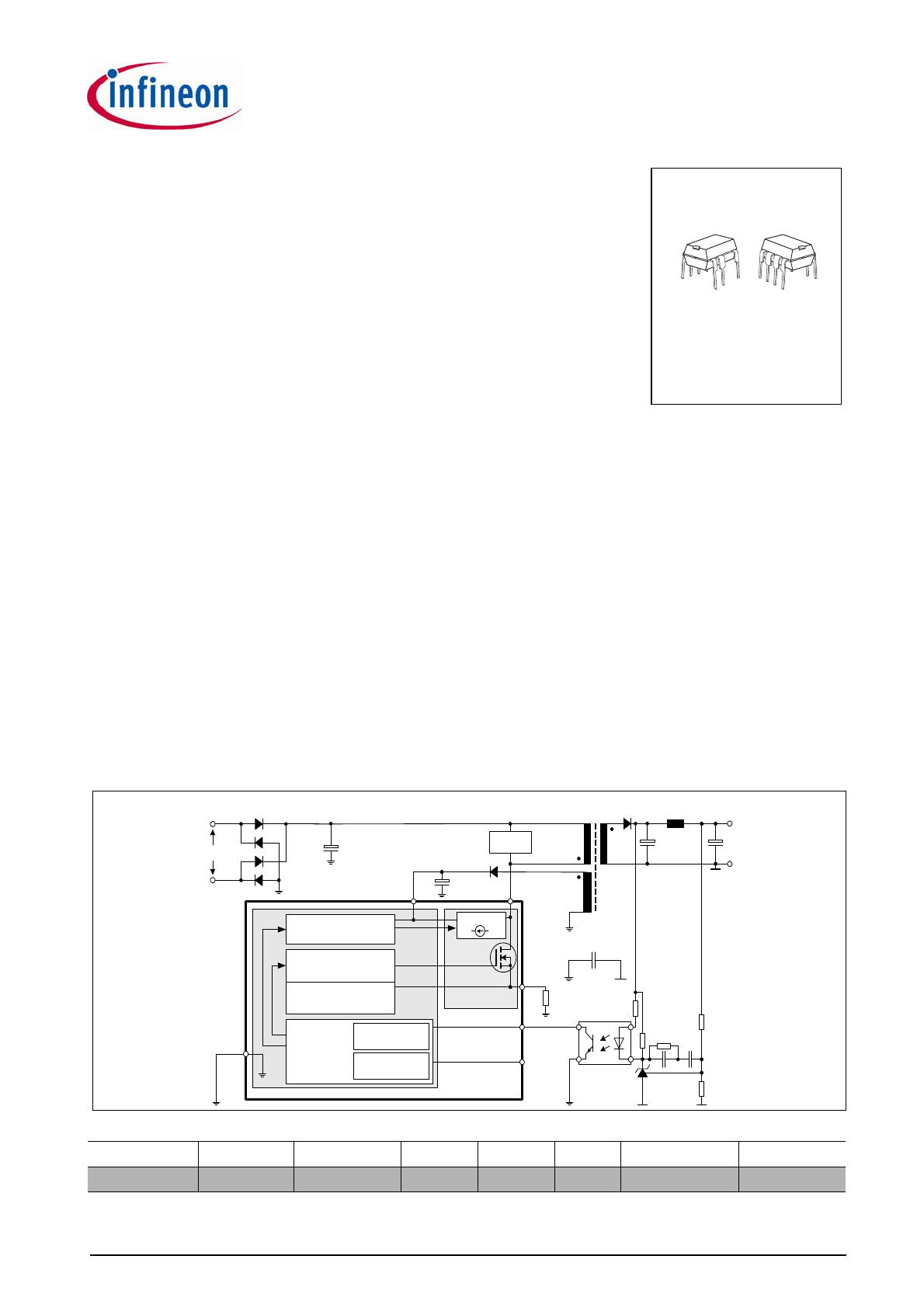
Power Management
PWM Controller
Current Mode
85 ... 270 VAC
Typical Application
R
Sense
BA
FB
GND
Active Burst Mode
Auto Restart Mode
Control
Unit
-
CS
VCC
Startup Cell
Precise Low Tolerance Peak
Current Limitation
Drain
CoolSET
®
-F3R
(Jitter Mode)
CoolMOS
®

ICE3RBR4765JZ
Table of Contents
Page
Version 2.0
4
7 Jun 2013
1
Pin Configuration and Functionality . . . . . . . . . . . . . . . . . . . . . . . . . . . . .6
1.1
Pin Configuration with PG-DIP-7 . . . . . . . . . . . . . . . . . . . . . . . . . . . . . . . . . .6
1.2
Pin Functionality . . . . . . . . . . . . . . . . . . . . . . . . . . . . . . . . . . . . . . . . . . . . . .6
2
Representative Blockdiagram . . . . . . . . . . . . . . . . . . . . . . . . . . . . . . . . . .7
3
Functional Description . . . . . . . . . . . . . . . . . . . . . . . . . . . . . . . . . . . . . . . .8
3.1
Introduction . . . . . . . . . . . . . . . . . . . . . . . . . . . . . . . . . . . . . . . . . . . . . . . . . .8
3.2
Power Management . . . . . . . . . . . . . . . . . . . . . . . . . . . . . . . . . . . . . . . . . . . .8
3.3
Improved Current Mode . . . . . . . . . . . . . . . . . . . . . . . . . . . . . . . . . . . . . . . . .9
3.3.1
PWM-OP . . . . . . . . . . . . . . . . . . . . . . . . . . . . . . . . . . . . . . . . . . . . . . . . .10
3.3.2
PWM-Comparator . . . . . . . . . . . . . . . . . . . . . . . . . . . . . . . . . . . . . . . . . .10
3.4
Startup Phase . . . . . . . . . . . . . . . . . . . . . . . . . . . . . . . . . . . . . . . . . . . . . . .11
3.5
PWM Section . . . . . . . . . . . . . . . . . . . . . . . . . . . . . . . . . . . . . . . . . . . . . . . .12
3.5.1
Oscillator . . . . . . . . . . . . . . . . . . . . . . . . . . . . . . . . . . . . . . . . . . . . . . . . .12
3.5.2
PWM-Latch FF1 . . . . . . . . . . . . . . . . . . . . . . . . . . . . . . . . . . . . . . . . . . . .12
3.5.3
Gate Driver . . . . . . . . . . . . . . . . . . . . . . . . . . . . . . . . . . . . . . . . . . . . . . .13
3.6
Current Limiting . . . . . . . . . . . . . . . . . . . . . . . . . . . . . . . . . . . . . . . . . . . . . .13
3.6.1
Leading Edge Blanking . . . . . . . . . . . . . . . . . . . . . . . . . . . . . . . . . . . . . .14
3.6.2
Propagation Delay Compensation . . . . . . . . . . . . . . . . . . . . . . . . . . . . . .14
3.7
Control Unit . . . . . . . . . . . . . . . . . . . . . . . . . . . . . . . . . . . . . . . . . . . . . . . . .15
3.7.1
Basic and Extendable Blanking Mode . . . . . . . . . . . . . . . . . . . . . . . . . . .15
3.7.2
Active Burst Mode . . . . . . . . . . . . . . . . . . . . . . . . . . . . . . . . . . . . . . . . . .15
3.7.2.1
Entering Active Burst Mode . . . . . . . . . . . . . . . . . . . . . . . . . . . . . . . . .15
3.7.2.2
Working in Active Burst Mode . . . . . . . . . . . . . . . . . . . . . . . . . . . . . . .16
3.7.2.3
Leaving Active Burst Mode . . . . . . . . . . . . . . . . . . . . . . . . . . . . . . . . .16
3.7.3
Protection Modes . . . . . . . . . . . . . . . . . . . . . . . . . . . . . . . . . . . . . . . . . . .17
3.7.3.1
Auto Restart mode with extended blanking time . . . . . . . . . . . . . . . . .17
3.7.3.2
Auto Restart without extended blanking time . . . . . . . . . . . . . . . . . . .18
4
Electrical Characteristics . . . . . . . . . . . . . . . . . . . . . . . . . . . . . . . . . . . . .19
4.1
Absolute Maximum Ratings . . . . . . . . . . . . . . . . . . . . . . . . . . . . . . . . . . . . .19
4.2
Operating Range . . . . . . . . . . . . . . . . . . . . . . . . . . . . . . . . . . . . . . . . . . . . .20
4.3
Characteristics . . . . . . . . . . . . . . . . . . . . . . . . . . . . . . . . . . . . . . . . . . . . . . .20
4.3.1
Supply Section . . . . . . . . . . . . . . . . . . . . . . . . . . . . . . . . . . . . . . . . . . . . .20
4.3.2
Internal Voltage Reference . . . . . . . . . . . . . . . . . . . . . . . . . . . . . . . . . . .21
4.3.3
PWM Section . . . . . . . . . . . . . . . . . . . . . . . . . . . . . . . . . . . . . . . . . . . . . .21
4.3.4
Soft Start time . . . . . . . . . . . . . . . . . . . . . . . . . . . . . . . . . . . . . . . . . . . . .21
4.3.5
Control Unit . . . . . . . . . . . . . . . . . . . . . . . . . . . . . . . . . . . . . . . . . . . . . . .22
4.3.6
Current Limiting . . . . . . . . . . . . . . . . . . . . . . . . . . . . . . . . . . . . . . . . . . . .23
4.3.7
CoolMOS
®
Section . . . . . . . . . . . . . . . . . . . . . . . . . . . . . . . . . . . . . . . . .23
5
Typical CoolMOS
®
Performance Characteristic . . . . . . . . . . . . . . . . . . .24

ICE3RBR4765JZ
Version 2.0
5
7 Jun 2013
6
Input Power Curve . . . . . . . . . . . . . . . . . . . . . . . . . . . . . . . . . . . . . . . . . . .26
7
Outline Dimension . . . . . . . . . . . . . . . . . . . . . . . . . . . . . . . . . . . . . . . . . . .27
8
Marking . . . . . . . . . . . . . . . . . . . . . . . . . . . . . . . . . . . . . . . . . . . . . . . . . . . .28
9
Schematic for recommended PCB layout . . . . . . . . . . . . . . . . . . . . . . . .29
Version 2.0
6
7 Jun 2013
ICE3RBR4765JZ
Pin Configuration and Functionality
1
Pin Configuration and Functionality
1.1
Pin Configuration with PG-DIP-7
Figure 1
Pin Configuration PG-DIP-7 (top view)
1.2
Pin Functionality
BA (extended Blanking & Auto-restart enable)
The BA pin combines the functions of extendable
blanking time for over load protection and the external
auto-restart enable. The extendable blanking time
function is to extend the built-in 20 ms blanking time by
adding an external capacitor at BA pin to ground. The
external auto-restart enable function is an external
access to stop the gate switching and force the IC enter
auto-restart mode. It is triggered by pulling down the
BA pin to less than 0.33V.
FB (Feedback)
The information about the regulation is provided by the
FB Pin to the internal Protection Unit and to the internal
PWM-Comparator to control the duty cycle. The FB-
Signal is the only control signal in case of light load at
the Active Burst Mode.
CS (Current Sense)
The Current Sense pin senses the voltage developed
on the series resistor inserted in the source of the
integrated CoolMOS
®
If voltage in CS pin reaches the
internal threshold of the Current Limit Comparator, the
Driver output is immediately switched off. Furthermore
the current information is provided for the PWM-
Comparator to realize the Current Mode.
Drain (Drain of integrated CoolMOS
®
)
Drain pin is the connection to the Drain of the
integrated CoolMOS
®
.
VCC (Power Supply)
VCC pin is the positive supply of the IC. The operating
range is between 10.5V and 25V.
GND (Ground)
GND pin is the ground of the controller.
Pin
Symbol
Function
1
BA
extended Blanking & Auto-restart
enable
2
FB
FeedBack
3
CS
Current Sense/
650V
1)
CoolMOS
®
Source
1)
at T
j
=110°C
4
n.c.
not connected
5
Drain
650V
1)
CoolMOS
®
Drain
6
n.c. Not
connected
7
VCC
Controller Supply Voltage
8
GND
Controller GrouND
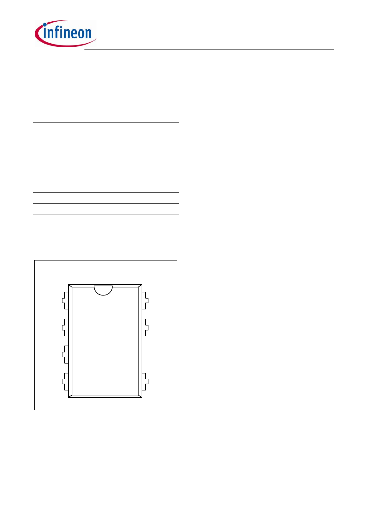
Package PG-DIP-7
1
7
8
4
3
2
5
GND
BA
FB
CS
VCC
n.c.
Drain
ICE3RBR4765JZ
Representative Blockdiagram
Version 2.0
7
7 Jun 2013
2
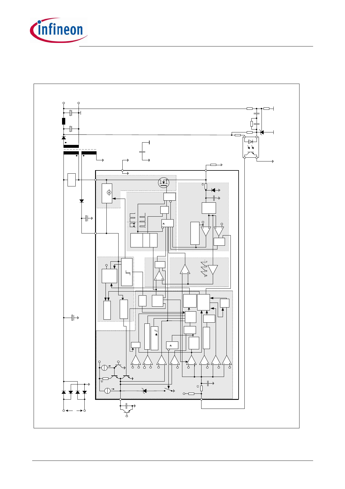
Representative Blockdiagram
Figure 2
Representative Blockdiagram
In
te
rn
a
l
B
ia
s
Vo
lt
a
g
e
Re
fe
re
n
c
e
O
s
c
illa
to
r
Du
ty
Cy
c
le
ma
x
x3
.2
C
u
rr
e
n
t
L
im
it
in
g
PWM
O
P
C
u
rre
n
t
M
o
d
e
So
ft
S
ta
rt
C2
C1
20.
5V
25.
5V
R
FB
P
o
w
e
r
M
an
ag
em
en
t
C
BK
C
VC
C
85
..
.
27
0
V
A
C
C
Bu
lk
+
Co
n
v
e
rt
e
r
DC
O
u
tp
u
t
V
OU
T
PWM
C
o
mp
ar
at
o
r
C3
4.
0
V
C4
4.
0
V
Ga
te
Dr
iv
e
r
0.
72
Cl
o
c
k
R
Se
n
se
10k
D1
C6
a
3.
0
V
C5
1.
3
5
V
C1
0
R
S
Q
Au
to
R
e
st
a
rt
Mo
de
&
G7
&
G5
&
G9
1
G8
& G1
T
her
ma
l
S
hu
td
o
w
n
0.
9
V
S1
1
P
o
w
e
r-D
ow
n
R
e
se
t
CS
BA
GND
VC
C
C7
C8
FB
PWM
Se
c
ti
o
n
C
o
nt
ro
l
U
ni
t
FF
1
C1
2
&
0.
34V
Le
ad
in
g
Ed
g
e
B
lan
k
ing
22
0ns
25
k
2pF
5.
0V
G1
0
1p
F
P
ropa
ga
ti
on
-D
e
lay
Co
m
p
e
n
s
a
ti
o
n
5.
0
V
U
n
d
e
rv
ol
ta
ge
Lo
c
k
o
u
t
V
cs
th
G2
-
ICE3
RBR
x
x
6
5
J
/
CoolSET
®
-F3
R
(
J
itte
r
M
ode
)
S
n
ubb
er
VCC
Dr
a
in
Coo
lM
O
S
®
St
a
rt
u
p
C
ell
C6
b
&
G6
3.
5V
&
G1
1
Ac
ti
v
e
Bu
rs
t
Mo
de
0.
6V
10
.5
V
18
V
#1
#
:
op
tion
al
e
x
te
rn
al
com
pon
ents
;
#1
:
C
BK
is
u
s
ed
to
e
x
te
nd
th
e
B
la
nk
in
g
T
im
e
#2
:
T
AE
is
us
ed
to
ena
ble
the
e
x
te
rn
al
A
u
to-
re
star
t
feat
ur
e
F
re
q
.
jit
te
r
20
ms
B
lan
k
ing
Ti
m
e
20m
s
B
la
nk
in
g
Ti
m
e
12
0us
B
lan
k
ing
T
im
e
So
ft
St
a
rt
Bl
o
c
k
S
o
ft
-S
ta
rt
C
o
mp
ar
at
o
r
Sp
ik
e
B
lank
in
g
30
us
T2
3.
25k
5.
0
V
T1
T3
0.
6
V
I
BK
VC
C
A
u
to
-r
es
ta
rt
En
a
b
le
S
ig
nal
T
AE
C9
0.
3
3
V
1m
s
co
u
n
te
r
T
j
>
1
30°
C
#2
Version 2.0
8
7 Jun 2013
ICE3RBR4765JZ
Functional Description
3
Functional Description
All values which are used in the functional description
are typical values. For calculating the worst cases the
min/max values which can be found in section 4
Electrical Characteristics have to be considered.
3.1
Introduction
ICE3RBR4765JZ (ICE3RBRxx65JZ series) is derived
from ICE3BRxx65J in DIP-7 package. It has more
robust design and can work to -40°C.
A high voltage Startup Cell is integrated into the IC
which is switched off once the Undervoltage Lockout
on-threshold of 18V is exceeded. This Startup Cell is
part of the integrated CoolMOS
®
. The external startup
resistor is no longer necessary as this Startup Cell is
connected to the Drain. Power losses are therefore
reduced. This increases the efficiency under light load
conditions drastically.
The particular features are the active burst mode,
propagation delay compensation, modulated gate
driving, auto-restart protection for Vcc overvoltage,
over temperature, over load, open loop, built-in soft
start, blanking window and frequency jitter. It provides
the flexibility to increase the blanking window by simply
addition of a capacitor in BA pin. In order to further
increase the flexibility of the protection feature, an
external auto-restart enable features are added.
The intelligent Active Burst Mode can effectively obtain
the lowest Standby Power at light load and no load
conditions. After entering the burst mode, there is still a
full control of the power conversion to the output
through the optocoupler, that is used for the normal
PWM control. The response on load jumps is optimized
and the voltage ripple on V
out
is minimized. The V
out
is
on well controlled in this mode.
The usually external connected RC-filter in the
feedback line after the optocoupler is integrated in the
IC to reduce the external part count.
Adopting the BiCMOS technology, it can increase the
design flexibility as the Vcc voltage range is increased
to 25V.
It has a built-in 20ms soft start function.
There are 2 modes of blanking time for high load
jumps; the basic mode and the extendable mode. The
blanking time for the basic mode is set at 20ms while
the extendable mode will increase the blanking time by
adding an external capacitor at the BA pin in addition to
the basic mode blanking time. During this blanking time
window the system can give the maximum power to the
loading.
In order to increase the robustness and safety of the
system, the IC provides Auto Restart protection. The
Auto Restart Mode reduces the average power
conversion to a minimum level under unsafe operating
conditions. This is necessary for a prolonged fault
condition which could otherwise lead to a destruction of
the SMPS over time. Once the malfunction is removed,
normal operation is automatically retained after the
next Start Up Phase. To make the protection more
flexible, an external auto-restart enable pin is provided.
When the pin is triggered, the switching pulse at gate
will stop and the IC enters the auto-restart mode after
the pre-defined spike blanking time.
The internal precise peak current control reduces the
costs for the transformer and the secondary diode. The
influence of the change in the input voltage on the
maximum power limitation can be avoided together
with the integrated Propagation Delay Compensation.
Therefore the maximum power is nearly independent
on the input voltage, which is required for wide range
SMPS. Thus there is no need for the over-sizing of the
SMPS, e.g. the transformer and the output diode.
Furthermore, it implements the frequency jitter mode to
the switching clock such that the EMI noise will be
effectively reduced.
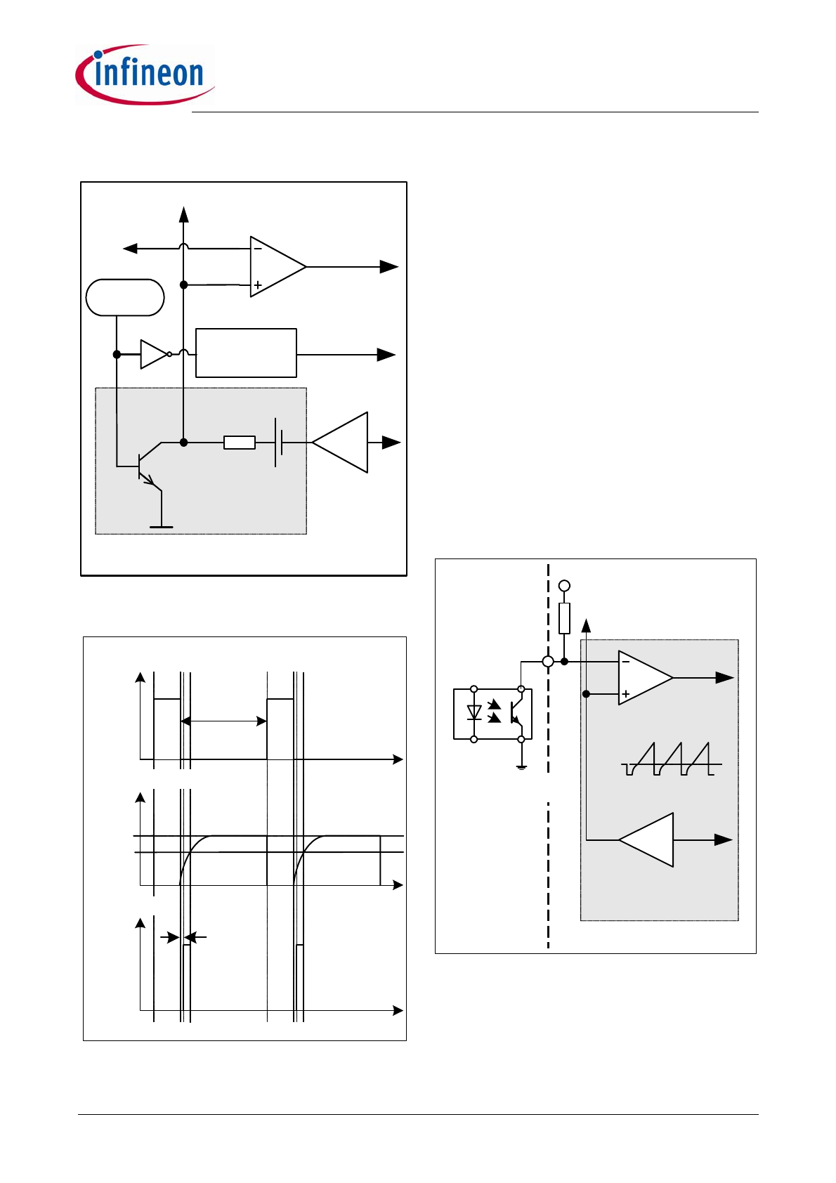
3.2
Power Management
Figure 3
Power Management
The Undervoltage Lockout monitors the external
supply voltage V
VCC
. When the SMPS is plugged to the
main line the internal Startup Cell is biased and starts
to charge the external capacitor C
VCC
which is
connected to the VCC pin. This VCC charge current is
Internal Bias
Voltage
Reference
Power Management
5.0V
Undervoltage Lockout
18V
10.5V
Power-Down Reset
Active Burst
Mode
Auto Restart
Mode
Startup Cell
VCC
Drain
CoolMOS
®
Soft Start block
ICE3RBR4765JZ
Functional Description
Version 2.0
9
7 Jun 2013
controlled to 0.9mA by the Startup Cell. When the V
VCC
exceeds the on-threshold V
CCon
=18V the bias circuit
are switched on. Then the Startup Cell is switched off
by the Undervoltage Lockout and therefore no power
losses present due to the connection of the Startup Cell
to the Drain voltage. To avoid uncontrolled ringing at
switch-on, a hysteresis start up voltage is implemented.
The switch-off of the controller can only take place
when V
VCC
falls below 10.5V after normal operation
was entered. The maximum current consumption
before the controller is activated is about 150
μA.
When V
VCC
falls below the off-threshold V
CCoff
=10.5V,
the bias circuit is switched off and the soft start counter
is reset. Thus it is ensured that at every startup cycle
the soft start starts at zero.
The internal bias circuit is switched off if Auto Restart
Mode is entered. The current consumption is then
reduced to 150
μA.
Once the malfunction condition is removed, this block
will then turn back on. The recovery from Auto Restart
Mode does not require re-cycling the AC line.
When Active Burst Mode is entered, the internal Bias is
switched off most of the time but the Voltage Reference
is kept alive in order to reduce the current consumption
below 450
μA.
3.3
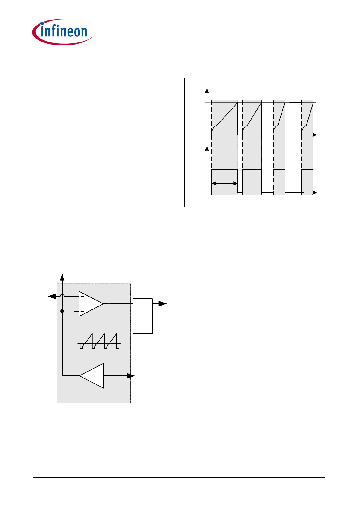
Improved Current Mode
Figure 4
Current Mode
Current Mode means the duty cycle is controlled by the
slope of the primary current. This is done by comparing
the FB signal with the amplified current sense signal.
Figure 5
Pulse Width Modulation
In case the amplified current sense signal exceeds the
FB signal the on-time T
on
of the driver is finished by
resetting the PWM-Latch (see Figure 5).
The primary current is sensed by the external series
resistor R
Sense
inserted in the source of the integrated
CoolMOS
®
. By means of Current Mode regulation, the
secondary output voltage is insensitive to the line
variations. The current waveform slope will change with
the line variation, which controls the duty cycle.
The external R
Sense
allows an individual adjustment of
the maximum source current of the integrated
CoolMOS
®
.
To improve the Current Mode during light load
conditions the amplified current ramp of the PWM-OP
is superimposed on a voltage ramp, which is built by
the switch T2, the voltage source V1 and a resistor R1
(see Figure 6). Every time the oscillator shuts down for
maximum duty cycle limitation the switch T2 is closed
by V
OSC
. When the oscillator triggers the Gate Driver,
T2 is opened so that the voltage ramp can start.
In case of light load the amplified current ramp is too
small to ensure a stable regulation. In that case the
Voltage Ramp is a well defined signal for the
comparison with the FB-signal. The duty cycle is then
controlled by the slope of the Voltage Ramp.
By means of the time delay circuit which is triggered by
the inverted V
OSC
signal, the Gate Driver is switched-off
until it reaches approximately 156ns delay time (see
Figure 7). It allows the duty cycle to be reduced
continuously till 0% by decreasing V
FB
below that
threshold.
x3.3
PWM OP
Improved
Current Mode
0.67V
C8
PWM-Latch
CS
FB
R
S
Q
Q
Driver
Soft-Start Comparator
t
FB
Amplified Current Signal
T
on
t
0.67V
Driver
ICE3RBR4765JZ
Functional Description
Version 2.0
10
7 Jun 2013
Figure 6
Improved Current Mode
Figure 7
Light Load Conditions
3.3.1
PWM-OP
The input of the PWM-OP is applied over the internal
leading edge blanking to the external sense resistor
R
Sense
connected to pin CS. R
Sense
converts the source
current into a sense voltage. The sense voltage is
amplified with a gain of 3.3 by PWM OP. The output of
the PWM-OP is connected to the voltage source V
1
.
The voltage ramp with the superimposed amplified
current signal is fed into the positive inputs of the PWM-
Comparator C8 and the Soft-Start-Comparator (see
Figure 6).
3.3.2
PWM-Comparator
The PWM-Comparator compares the sensed current
signal of the integrated CoolMOS
®
with the feedback
signal V
FB
(see Figure 8). V
FB
is created by an external
optocoupler or external transistor in combination with
the internal pull-up resistor R
FB
and provides the load
information of the feedback circuitry. When the
amplified current signal of the integrated CoolMOS
®
exceeds the signal V
FB
the PWM-Comparator switches
off the Gate Driver.
Figure 8
PWM Controlling
PWM OP
0.67V
10k
Ω
Oscillator
C8
T
2
R
1
FB
PWM-Latch
V
1
Gate Driver
Voltage Ramp
V
OSC
Soft-Start Comparator
time delay
circuit (156ns)
PWM Comparator
X3.3
t
t
V
OSC
0.67V
FB
t
max.
Duty Cycle
Gate Driver
Voltage Ramp
156ns time delay
X3.3
PWM OP
Improved
Current Mode
PWM Comparator
CS
Soft-Start Comparator
5V
C8
0.67V
FB
Optocoupler
R
FB
PWM-Latch