

CoolSET
®
-F3R80
ICE3AR2280JZ-T
Off-Line SMPS Current Mode
Controller with integrated 800V
CoolMOS
®
and Startup cell
(brownout & frequency jitter) in
DIP-7
N e v e r
s t o p
t h i n k i n g .
Power Management & Supply
Version 2.0, 20 Mar 2013

Edition 2013-03-20
Published by
Infineon Technologies AG
81726 München, Germany
©
Infineon Technologies AG 3/20/13.
All Rights Reserved.
Attention please!
The information given in this data sheet shall in no event be regarded as a guarantee of conditions or
characteristics (“Beschaffenheitsgarantie”). With respect to any examples or hints given herein, any typical values
stated herein and/or any information regarding the application of the device, Infineon Technologies hereby
disclaims any and all warranties and liabilities of any kind, including without limitation warranties of
non-infringement of intellectual property rights of any third party.
Information
For further information on technology, delivery terms and conditions and prices please contact your nearest
Infineon Technologies Office (
www.infineon.com
).
Warnings
Due to technical requirements components may contain dangerous substances. For information on the types in
question please contact your nearest Infineon Technologies Office.
Infineon Technologies Components may only be used in life-support devices or systems with the express written
approval of Infineon Technologies, if a failure of such components can reasonably be expected to cause the failure
of that life-support device or system, or to affect the safety or effectiveness of that device or system. Life support
devices or systems are intended to be implanted in the human body, or to support and/or maintain and sustain
and/or protect human life. If they fail, it is reasonable to assume that the health of the user or other persons may
be endangered.
For questions on technology, delivery and prices please contact the Infineon Technologies Offices in Germany or
the Infineon Technologies Companies and Representatives worldwide: see our webpage at http://
www.infineon.com
CoolMOS
®
, CoolSET
®
are trademarks of Infineon Technologies AG.
CoolSET
®
-F3R80
ICE3AR2280JZ-T
Revision History:
2013-03-20
Datasheet Version 2.0
Previous Version: 0.0
Page
Subjects (major changes since last revision)
Type
Package
Marking
V
DS
F
OSC
R
DSon
1)
1)
typ @ T=25°C
230VAC ±15%
2)
2)
Calculated maximum input power rating at T
a
=50°C, T
i
=125°C and without copper area as heat sink.
85-265 VAC
2)
ICE3AR2280JZ-T
PG-DIP-7
3AR2280JZ-T
800V
100kHz
2.26
43W
28W
CoolSET
®
-F3R80
ICE3AR2280JZ-T
Version 2.0
3
20 Mar 2013
Off-Line SMPS Current Mode Controller with
integrated 800V CoolMOS
®
and Startup cell
(brownout & frequency jitter) in DIP-7
PG-DIP7
Features
• 800V avalanche rugged CoolMOS
®
with Startup Cell
• Active Burst Mode for lowest Standby Power
• Selectable entry and exit burst mode level
• 100kHz internally fixed switching frequency with
jittering feature
• Auto Restart Protection for Over load, Open Loop,
VCC Under voltage & Over voltage and Over
temperature
• External auto-restart enable pin
• Over temperature protection with 50°C hysteresis
• Built-in 10ms Soft Start
• Built-in 20ms and extendable blanking time for short
duration peak power
• Propagation delay compensation for both maximum
load and burst mode
• Adjustable brownout feature
• Overall tolerance of Current Limiting < ±5%
• BiCMOS technology for low power consumption and
wide VCC voltage range
• Soft gate drive with 50W turn on resistor
Description
The
ICE3AR2280JZ-T
(CoolSET
®
-F3R80)
is
an
enhanced 800V MOSFET version of ICE3BRxx65J
(CoolSET
®
-F3R 650V) in DIP-7 package. The PWM
controller is based on F3R 650V with some new and
enhanced features. In particular it is a device running at
100KHz, implemented with brownout features, installing
800V CoolMOS
®
with startup cell and packaged into DIP-
7. It targets for the low power SMPS with increased
MOSFET voltage margin requirement such as Off-Line
battery adapters, DVD R/W, DVD Combi, Blue ray, set top
box, auxiliary power supply for PC and server, etc. In
summary, the CoolSET
®
F3R80 provides good voltage
margin of MOSFET, lowest standby power, selectable
burst level, reduced output ripple during burst mode,
reliable output with brownout feature, accurate maximum
power control for both maximum power and burst power,
low EMI with frequency jittering and soft gate drive, built-
in and flexible protections, etc. Therefore, CoolSET
®
F3R80 is a complete solution for the low power SMPS
application.
Product Highlights
• 800V avalanche rugged CoolMOS
®
with startup cell
• Active Burst Mode to reach the lowest Standby Power <100mW
• Selectable entry and exit burst mode level
• Adjustable blanking Window for high load jumps
• Frequency jitter and soft driving for low EMI
• Adjustable brownout feature
• Auto Restart protection for over load, over temperature, over voltage and
external protection enable function
• Low operating temperature down to -40°C
• Pb-free lead plating; RoHS compliant
C
VCC
C
Bulk
Converter
DC Output
+
Snubber
Power Management
PWM Controller
Current Mode
85 ... 270 VAC
Typical Application
R
Sense
FBB
Control Unit
-
CS
VCC
Startup Cell
Precise Low Tolerance Peak
Current Limitation
Drain
CoolSET
®
-F3R80
(Brownout & Jitter)
CoolMOS
®
GND
R
BO2
R
BO1
Active Burst Mode
Auto Restart Mode
Brownout mode
BBA

CoolSET
®
-F3R80
ICE3AR2280JZ-T
Table of Contents
Page
Version 2.0
4
20 Mar 2013
1
Pin Configuration and Functionality . . . . . . . . . . . . . . . . . . . . . . . . . . . . .6
1.1
Pin Configuration with PG-DIP-7 . . . . . . . . . . . . . . . . . . . . . . . . . . . . . . . . . .6
1.2
Pin Functionality . . . . . . . . . . . . . . . . . . . . . . . . . . . . . . . . . . . . . . . . . . . . . .6
2
Representative Blockdiagram . . . . . . . . . . . . . . . . . . . . . . . . . . . . . . . . . .7
3
Functional Description . . . . . . . . . . . . . . . . . . . . . . . . . . . . . . . . . . . . . . . .8
3.1
Introduction . . . . . . . . . . . . . . . . . . . . . . . . . . . . . . . . . . . . . . . . . . . . . . . . . .8
3.2
Power Management . . . . . . . . . . . . . . . . . . . . . . . . . . . . . . . . . . . . . . . . . . . .8
3.3
Improved Current Mode . . . . . . . . . . . . . . . . . . . . . . . . . . . . . . . . . . . . . . . . .9
3.3.1
PWM-OP . . . . . . . . . . . . . . . . . . . . . . . . . . . . . . . . . . . . . . . . . . . . . . . . .10
3.3.2
PWM-Comparator . . . . . . . . . . . . . . . . . . . . . . . . . . . . . . . . . . . . . . . . . .10
3.4
Startup Phase . . . . . . . . . . . . . . . . . . . . . . . . . . . . . . . . . . . . . . . . . . . . . . .10
3.5
PWM Section . . . . . . . . . . . . . . . . . . . . . . . . . . . . . . . . . . . . . . . . . . . . . . . .12
3.5.1
Oscillator . . . . . . . . . . . . . . . . . . . . . . . . . . . . . . . . . . . . . . . . . . . . . . . . .12
3.5.2
PWM-Latch FF1 . . . . . . . . . . . . . . . . . . . . . . . . . . . . . . . . . . . . . . . . . . . .12
3.5.3
Gate Driver . . . . . . . . . . . . . . . . . . . . . . . . . . . . . . . . . . . . . . . . . . . . . . .12
3.6
Current Limiting . . . . . . . . . . . . . . . . . . . . . . . . . . . . . . . . . . . . . . . . . . . . . .13
3.6.1
Leading Edge Blanking . . . . . . . . . . . . . . . . . . . . . . . . . . . . . . . . . . . . . .13
3.6.2
Propagation Delay Compensation (patented) . . . . . . . . . . . . . . . . . . . . .13
3.7
Control Unit . . . . . . . . . . . . . . . . . . . . . . . . . . . . . . . . . . . . . . . . . . . . . . . . .14
3.7.1
Basic and Extendable Blanking Mode . . . . . . . . . . . . . . . . . . . . . . . . . . .14
3.7.2
Active Burst Mode (patented) . . . . . . . . . . . . . . . . . . . . . . . . . . . . . . . . .15
3.7.2.1
Selectable burst entry level . . . . . . . . . . . . . . . . . . . . . . . . . . . . . . . . .15
3.7.2.2
Entering Active Burst Mode . . . . . . . . . . . . . . . . . . . . . . . . . . . . . . . . .16
3.7.2.3
Working in Active Burst Mode . . . . . . . . . . . . . . . . . . . . . . . . . . . . . . .16
3.7.2.4
Leaving Active Burst Mode . . . . . . . . . . . . . . . . . . . . . . . . . . . . . . . . .16
3.7.3
Protection Modes . . . . . . . . . . . . . . . . . . . . . . . . . . . . . . . . . . . . . . . . . . .17
3.7.3.1
Vcc OVP, OTP, external protection enable and Vcc under voltage . . .18
3.7.3.2
Over load, open loop protection . . . . . . . . . . . . . . . . . . . . . . . . . . . . . .18
3.7.4
Brownout Mode . . . . . . . . . . . . . . . . . . . . . . . . . . . . . . . . . . . . . . . . . . . .19
3.7.5
Action sequence at BBA pin . . . . . . . . . . . . . . . . . . . . . . . . . . . . . . . . . .20
4
Electrical Characteristics . . . . . . . . . . . . . . . . . . . . . . . . . . . . . . . . . . . . .22
4.1
Absolute Maximum Ratings . . . . . . . . . . . . . . . . . . . . . . . . . . . . . . . . . . . . .22
4.2
Operating Range . . . . . . . . . . . . . . . . . . . . . . . . . . . . . . . . . . . . . . . . . . . . .23
4.3
Characteristics . . . . . . . . . . . . . . . . . . . . . . . . . . . . . . . . . . . . . . . . . . . . . . .23
4.3.1
Supply Section . . . . . . . . . . . . . . . . . . . . . . . . . . . . . . . . . . . . . . . . . . . . .23
4.3.2
Internal Voltage Reference . . . . . . . . . . . . . . . . . . . . . . . . . . . . . . . . . . .24
4.3.3
PWM Section . . . . . . . . . . . . . . . . . . . . . . . . . . . . . . . . . . . . . . . . . . . . . .24
4.3.4
Soft Start time . . . . . . . . . . . . . . . . . . . . . . . . . . . . . . . . . . . . . . . . . . . . .24
4.3.5
Control Unit . . . . . . . . . . . . . . . . . . . . . . . . . . . . . . . . . . . . . . . . . . . . . . .25
4.3.6
Current Limiting . . . . . . . . . . . . . . . . . . . . . . . . . . . . . . . . . . . . . . . . . . . .26
4.3.7
CoolMOS
®
Section . . . . . . . . . . . . . . . . . . . . . . . . . . . . . . . . . . . . . . . . .26

CoolSET
®
-F3R80
ICE3AR2280JZ-T
Version 2.0
5
20 Mar 2013
5
CoolMOS
®
Performance Characteristic . . . . . . . . . . . . . . . . . . . . . . . . . .27
6
Input Power Curve . . . . . . . . . . . . . . . . . . . . . . . . . . . . . . . . . . . . . . . . . . .29
7
Outline Dimension . . . . . . . . . . . . . . . . . . . . . . . . . . . . . . . . . . . . . . . . . . .30
8
Marking . . . . . . . . . . . . . . . . . . . . . . . . . . . . . . . . . . . . . . . . . . . . . . . . . . . .31
9
Schematic for recommended PCB layout . . . . . . . . . . . . . . . . . . . . . . . .32
Version 2.0
6
20 Mar 2013
CoolSET
®
-F3R80
ICE3AR2280JZ-T
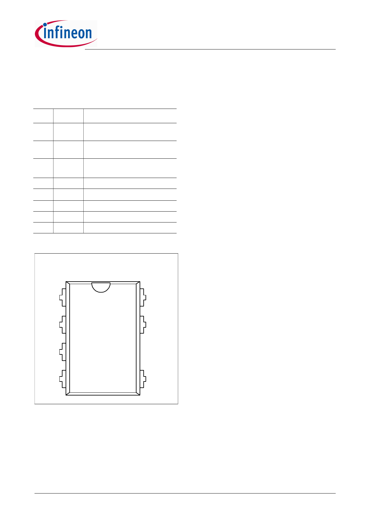
Pin Configuration and Functionality
1
Pin Configuration and Functionality
1.1
Pin Configuration with PG-DIP-7
Figure 1
Pin Configuration PG-DIP-7 (top view)
1.2
Pin Functionality
BBA (Brownout, extended Blanking time & Auto-
restart enable)
The BBA pin combines the functions of brownout,
extendable blanking time for over load protection and
the external auto-restart enable. The brownout feature
is to stop the switching pulse when the input voltage is
dropped to a preset low level. The extendable blanking
time function is to extend the built-in 20 ms blanking
time for over load protection by adding an external
capacitor to ground. The external auto-restart enable
function is an external access to stop the gate
switching and force the IC to enter auto-restart mode.
It is triggered by pulling the pin voltage to less than
0.4V.
FBB (Feedback & Burst entry control)
The FBB pin combines the feedback function and the
burst entry/exit control. The regulation information is
provided by the FBB pin to the internal Protection Unit
and the internal PWM-Comparator to control the duty
cycle. The FBB-signal is the only control signal in case
of light load at the Active Burst Mode. The burst entry/
exit control provides an access to select the entry/exit
burst mode level.
CS (Current Sense)
The Current Sense pin senses the voltage developed
on the shunt resistor inserted in the source of the
integrated CoolMOS
®
. If CS reaches the internal
threshold of the Current Limit Comparator, the Driver
output is immediately switched off. Furthermore the
current information is provided for the PWM-
Comparator to realize the Current Mode.
Drain (Drain of integrated CoolMOS
®
)
Pin Drain is the connection to the Drain of the
integrated CoolMOS
®
.
VCC (Power Supply)
The VCC pin is the positive supply of the IC. The
operating range is between 10.5V and 25V.
GND (Ground)
The GND pin is the ground of the controller.
Pin
Symbol
Function
1
BBA
Brownout, extended Blanking
time & Auto-restart enable
2
FBB
Feedback & Burst entry/exit con-
trol
3
CS
Current Sense/
800V CoolMOS
®
Source
4
n.c.
not connected
5
Drain
800V CoolMOS
®
Drain
6
-
(no pin)
7
VCC
Controller Supply Voltage
8
GND
Controller Ground
Package PG-DIP-7
1
7
8
4
3
2
5
GND
BBA
FBB
CS
VCC
n.c.
Drain
CoolSET
®
-F3R80
ICE3AR2280JZ-T
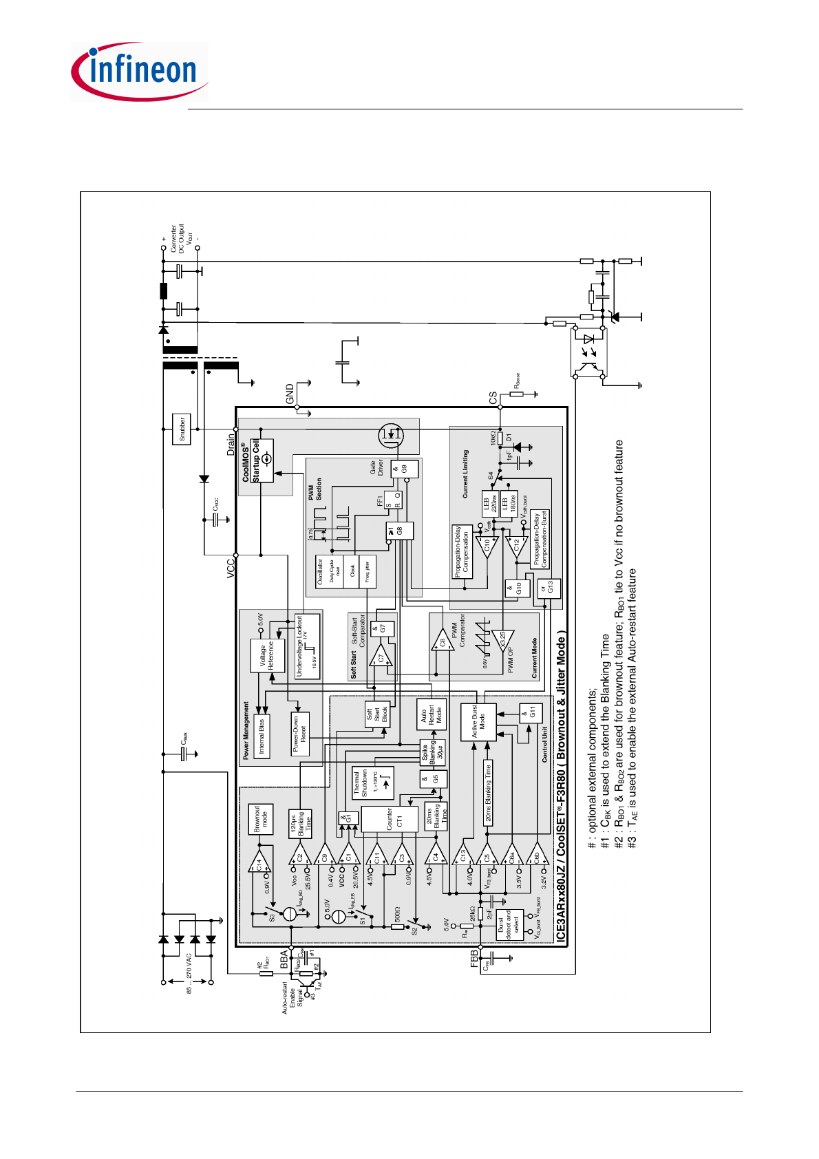
Representative Blockdiagram
Version 2.0
7
20 Mar 2013
2
Representative Blockdiagram
Figure 2
Representative Blockdiagram
Version 2.0
8
20 Mar 2013
CoolSET
®
-F3R80
ICE3AR2280JZ-T
Functional Description
3
Functional Description
All values which are used in the functional description
are typical values. For calculating the worst cases the
min/max values which can be found in section 4
Electrical Characteristics have to be considered.
3.1
Introduction
CoolSET
®
-F3R80 brownout and jitter 800V version
(ICE3AR2280JZ-T) is the enhanced version of the
CoolSET
®
-F3R 650V version (ICE3BRxx65J). It is
particular good for high voltage margin low power
SMPS application such as auxiliary power supply for
PC and server. The major characteristics are that the
IC is developed with 800V CoolMOS
®
with start up cell,
having adjustable brownout feature, running at 100KHz
switching frequency and packed in DIP-7 package. It is
derived from F3R 650V version. Thus most of the good
features are retained. Besides, it includes some
enhanced features and new features.
The
retained
good
features
include
BiCMOS
technology to reduce power consumption and increase
the Vcc voltage range, cycle by cycle current mode
control, built-in 10ms soft start to reduce the stress of
switching elements during start up, built-in 20ms and
extended blanking time for short period of peak power
before entering protection, active burst mode for lowest
standby power and propagation delay compensation
for close power limit between high line and low line,
frequency jittering for low EMI performance, the built-in
auto-restart mode protections for open loop, over load,
Vcc OVP, Vcc under voltage, etc. and also the most
flexible external auto-restart enable, etc.
The enhanced features include narrowing the feedback
voltage swing from 0.5V to 0.3V during burst mode so
that the output voltage ripple can be reduced by 40%,
reduction of the fast voltage fall time of the MOSFET by
increasing the soft turn-on time and addition of 50W
turn-on resistor, faster start up time by optimizing the
Vcc capacitor to 10uF and over temperature protection
with 50°C hysteresis.
The new features include adjustable brownout for
reliable output performance, selectable entry and exit
burst mode so that smaller entry/exit power to burst
mode or even no burst mode is possible and the
propagation delay compensation for burst mode so that
the entry/exit burst mode power is close between high
line and low line.
In summary, the CoolSET
®
F3R80 provides good
voltage margin of MOSFET, lowest standby power,
flexible burst level, reduced output ripple during burst
mode, reliable output with brownout feature, accurate
power limit for both maximum power and burst power,
low EMI with frequency jittering and soft gate drive,
built-in and flexible protections, etc. Therefore,
CoolSET
®
F3R80 is a complete solution for the low
power SMPS application.
3.2
Power Management
Figure 3
Power Management
The Undervoltage Lockout monitors the external
supply voltage V
VCC
. When the SMPS is plugged to the
main line the internal Startup Cell is biased and starts
to charge the external capacitor C
VCC
which is
connected to the VCC pin. This VCC charge current is
controlled to 0.9mA by the Startup Cell. When the V
VCC
exceeds the on-threshold V
CCon
=17V the bias circuit
are switched on. Then the Startup Cell is switched off
by the Undervoltage Lockout and therefore no power
losses present due to the connection of the Startup Cell
to the Drain voltage. To avoid uncontrolled ringing at
switch-on, a hysteresis start up voltage is implemented.
The switch-off of the controller can only take place
when V
VCC
falls below 10.5V after normal operation
was entered. The maximum current consumption
before the controller is activated is about 200mA.
When V
VCC
falls below the off-threshold V
CCoff
=10.5V,
the bias circuit is switched off and the soft start counter
is reset. Thus it ensures that at every startup cycle the
soft start starts at zero.
The internal bias circuit is switched off if Auto Restart
Mode is entered. The current consumption is then
reduced to 320mA.
Internal Bias
Voltage
Reference
Power Management
5.0V
Undervoltage Lockout
17V
10.5V
Power-Down Reset
Active Burst
Mode
Auto Restart
Mode
Startup Cell
VCC
Drain
CoolMOS
®
Soft Start block
CoolSET
®
-F3R80
ICE3AR2280JZ-T
Functional Description
Version 2.0
9
20 Mar 2013
Once the malfunction condition is removed, this block
will then turn back on. The recovery from Auto Restart
Mode does not require re-cycling the AC line.
When Active Burst Mode is entered, the internal Bias is
switched off most of the time but the Voltage Reference
is kept alive in order to reduce the current consumption
below 620mA.
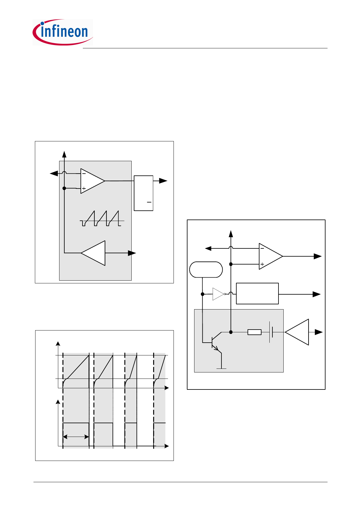
3.3
Improved Current Mode
Figure 4
Current Mode
Current Mode means the duty cycle is controlled by the
slope of the primary current. This is done by comparing
the FBB signal with the amplified current sense signal.
Figure 5
Pulse Width Modulation
In case the amplified current sense signal exceeds the
FBB signal the on-time t
on
of the driver is finished by
resetting the PWM-Latch (Figure 5).
The primary current is sensed by the external series
resistor R
Sense
inserted in the source of the integrated
CoolMOS
®
. By means of Current Mode regulation, the
secondary output voltage is insensitive to the line
variations. The current waveform slope will change with
the line variation, which controls the duty cycle.
The external R
Sense
allows an individual adjustment of
the maximum source current of the integrated
CoolMOS
®
.
To improve the Current Mode during light load
conditions the amplified current ramp of the PWM-OP
is superimposed on a voltage ramp, which is built by
the switch T2, the voltage source V1 and a resistor R1
(see Figure 6). Every time the oscillator shuts down for
maximum duty cycle limitation the switch T2 is closed
by V
OSC
. When the oscillator triggers the Gate Driver,
T2 is opened so that the voltage ramp can start.
Figure 6
Improved Current Mode
In case of light load the amplified current ramp is too
small to ensure a stable regulation. In that case the
Voltage Ramp is a well defined signal for the
comparison with the FBB-signal. The duty cycle is then
controlled by the slope of the Voltage Ramp.
By means of the time delay circuit which is triggered by
the inverted V
OSC
signal, the Gate Driver is switched-off
until it reaches approximately 156ns delay time (Figure
x3.25
PWM OP
Improved
Current Mode
0.6V
C8
PWM-Latch
CS
FBB
R
S
Q
Q
Driver
Soft-Start Comparator
t
FBB
Amplified Current Signal
t
on
t
0.6V
Driver
PWM OP
0.6V
10k
Oscillator
C8
T
2
R
1
FBB
PWM-Latch
V
1
Gate Driver
Voltage Ramp
V
OSC
Soft-Start Comparator
time delay
circuit (156ns)
X3.25
PWM Comparator
CoolSET
®
-F3R80
ICE3AR2280JZ-T
Functional Description
Version 2.0
10
20 Mar 2013
7). It allows the duty cycle to be reduced continuously
till 0% by decreasing V
FBB
below that threshold.
Figure 7
Light Load Conditions
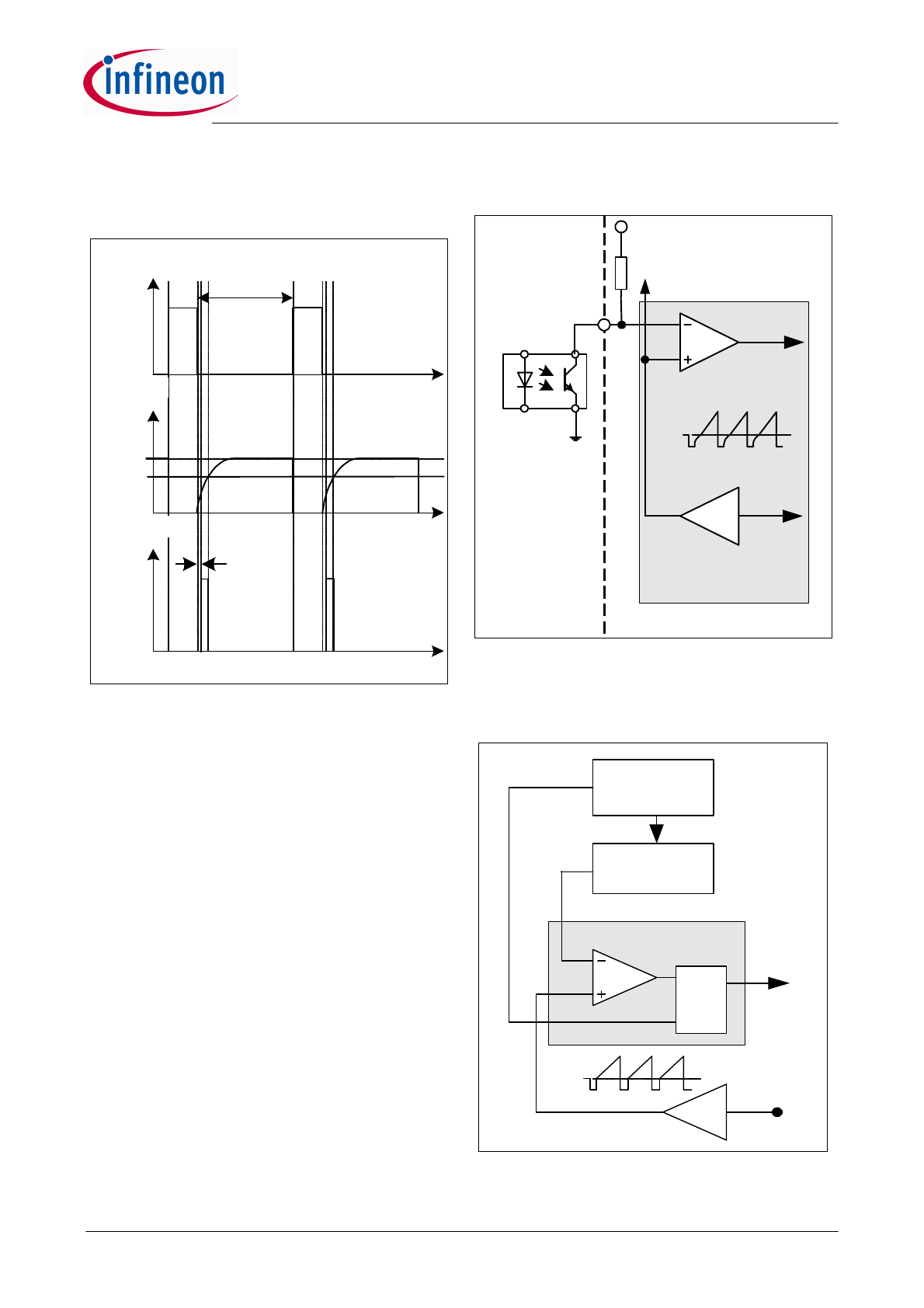
3.3.1
PWM-OP
The input of the PWM-OP is applied over the internal
leading edge blanking to the external sense resistor
R
Sense
connected to pin CS. R
Sense
converts the source
current into a sense voltage. The sense voltage is
amplified with a gain of 3.25 by PWM OP. The output
of the PWM-OP is connected to the voltage source V
1
.
The voltage ramp with the superimposed amplified
current signal is fed into the positive inputs of the PWM-
Comparator C8 and the Soft-Start-Comparator (Figure
8).
3.3.2
PWM-Comparator
The PWM-Comparator compares the sensed current
signal of the integrated CoolMOS
®
with the feedback
signal V
FBB
(Figure 8). V
FBB
is created by an external
optocoupler or external transistor in combination with
the internal pull-up resistor R
FB
and provides the load
information of the feedback circuitry. When the
amplified current signal of the integrated CoolMOS
®
exceeds the signal V
FBB
the PWM-Comparator
switches off the Gate Driver.
Figure 8
PWM Controlling
3.4
Startup Phase
Figure 9
Soft Start
t
t
V
OSC
0.6V
FBB
t
max.
Duty Cycle
Gate
Driver
Voltage
Ramp
156ns time delay
X3.25
PWM OP
Improved
Current Mode
PWM Comparator
CS
Soft-Start Comparator
5V
C8
0.6V
FBB
Optocoupler
R
FB
PWM-Latch
Soft-Start
C om parator
Soft Start
&
G 7
C 7
G ate D river
0.6V
x3.25
PW M O P
C S
Soft Start counter
Soft Start
S
o
ft
S
ta
rt
fi
n
is
h
SoftS