

C o o l S E T
®
-Q1
I C E 2 Q R 4 7 6 5
O f f - L i n e S M P S Q u a s i - R e s o n a n t
P W M C o n t r o l l e r w i t h i n t e g r a t e d
6 5 0 V C o o l M O S
®
a n d s t a r t u p c e l l i n
D I P - 8
N e v e r s t o p t h i n k i n g .
P o w e r M a n a g e m e n t & S u p p l y
D a t a s h e e t , V e r s i o n 2 . 3 , N o v e m b e r 1 4 , 2 0 1 2

Edition 2012-11-14
Published by
Infineon Technologies AG
81726 München, Germany
©
Infineon Technologies AG 11/14/12.
All Rights Reserved.
Attention please!
The information given in this data sheet shall in no event be regarded as a guarantee of conditions or
characteristics (“Beschaffenheitsgarantie”). With respect to any examples or hints given herein, any typical values
stated herein and/or any information regarding the application of the device, Infineon Technologies hereby
disclaims any and all warranties and liabilities of any kind, including without limitation warranties of
non-infringement of intellectual property rights of any third party.
Information
For further information on technology, delivery terms and conditions and prices please contact your nearest
Infineon Technologies Office (
www.infineon.com
).
Warnings
Due to technical requirements components may contain dangerous substances. For information on the types in
question please contact your nearest Infineon Technologies Office.
Infineon Technologies Components may only be used in life-support devices or systems with the express written
approval of Infineon Technologies, if a failure of such components can reasonably be expected to cause the failure
of that life-support device or system, or to affect the safety or effectiveness of that device or system. Life support
devices or systems are intended to be implanted in the human body, or to support and/or maintain and sustain
and/or protect human life. If they fail, it is reasonable to assume that the health of the user or other persons may
be endangered.
For questions on technology, delivery and prices please contact the Infineon Technologies Offices in Germany or
the Infineon Technologies Companies and Representatives worldwide: see our webpage at http://
www.infineon.com
CoolMOS
®
, CoolSET
®
are trademarks of Infineon Technologies AG.
CoolSET
®
-Q1
ICE2QR4765
Revision History:
November 14, 2012
Datasheet
Previous Version:
2.2
Page
Subjects (major changes since last revision)
20
Revised outline dimension.
21
Add marking
Type
Package
Marking
V
DS
R
DSon
1)
1)
typ @ T=25°C
230VAC ±15%
2)
2)
Calculated maximum input power rating at T
a
=50°C, T
i
=125°C and without copper area as heat sink.
85-265 VAC
2)
ICE2QR4765
PG-DIP-8
ICE2QR4765
650V
4.7
30W
19W
CoolSET
®
-Q1
ICE2QR4765
Version 2.3
3
November 14, 2012
Off-Line SMPS Quasi-Resonant PWM
Controller with integrated 650V CoolMOS
®
and startup cell in DIP-8
PG-DIP-8
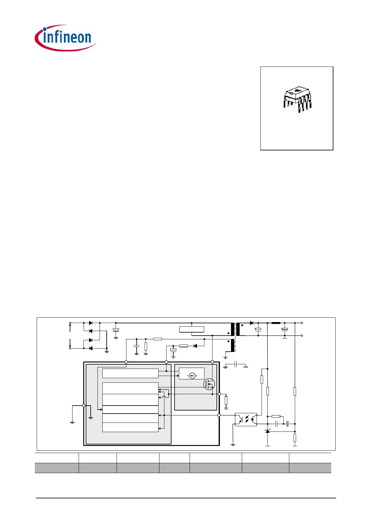
Description
The CoolSET
®
-Q1 series (ICE2QRxx65) is the first
generation of quasi-resonant integarted power ICs. It is
optimized for off-line switch mode power supply
applications such as LCD monitor, DVD R/W, DVD
Combo, Blue-ray DVD, set top box, etc. Operting the
MOSFET switch in quasi-resonant mode, lower EMI,
higher efficiency and lower voltage stress on secondary
diodes are expected for the SMPS. Based on the
BiCMOS technology, the CoolSET
®
-Q1 series has a
wide operation range (up to 25V) of IC power supply
and lower power consumption. It also offers many
advantages such as: a quasi-resonant operation till very
low load increasing the average system efficiency
compared to other conventional solutions; the Active
Burst Mode operation enables an ultra-low power
consumption at standby mode with small and
controllable output voltage ripple.
Product Highlights
•
Active Burst Mode to reach the lowest standby power requirement
<100mW@no load
•
Quasi resonant operation
•
Digital frequency reduction for better overall system efficiency
•
Integrated 650V startup cell
Features
•
650V avalanche rugged CoolMOS
®
with built-in
startup cell
•
Quasiresonant operation till very low load
•
Active burst mode operation for low standby input
power (< 0.1W)
•
Digital frequency reduction with decreasing load for
reduced switching loss
•
Built-in digital soft-start
•
Foldback point correction and cycle-by-cycle peak
current limitation
•
Maximum on time limitation
•
Auto restart mode for VCC Overvoltage and
Undervoltage protections
•
Auto restart mode for overload protection
•
Auto restart mode for overtemperature protection
•
Latch-off mode for adjustable output overvoltage
protection and transformer short-winding protection
85 ~ 265 VAC
Snubber
C
bus
D
r1
~D
r4
R
CS
TL431
Optocoupler
R
b1
R
b2
R
c1
C
c1
C
c2
R
ovs2
R
ovs1
C
VCC
D
VCC
D
O
C
O
L
f
C
f
V
O
C
PS
Startup Cell
CoolSET
®
-Q1
Depl. CoolMOS
®
Power Cell
W
p
W
s
W
a
R
VCC
C
ZC
R
ZC2
R
ZC1
Drain
Zero Crossing Block
Power Management
Cycle-by-Cycle
current limitation
Active Burst Mode
PWM controller
Current Mode Control
Protections
VCC
CS
Control Unit
ZC
FB
GND

CoolSET
®
- Q1
ICE2QR4765
Table of Contents
Page
Version 2.3
4
November 14, 2012
1
Pin Configuration and Functionality . . . . . . . . . . . . . . . . . . . . . . . . . . . . .5
1.1
Pin Configuration with PG-DIP-8 . . . . . . . . . . . . . . . . . . . . . . . . . . . . . . . . . .5
1.2
Package PG-DIP-8 . . . . . . . . . . . . . . . . . . . . . . . . . . . . . . . . . . . . . . . . . . . .5
1.3
Pin Functionality . . . . . . . . . . . . . . . . . . . . . . . . . . . . . . . . . . . . . . . . . . . . . .5
2
Representative Blockdiagram . . . . . . . . . . . . . . . . . . . . . . . . . . . . . . . . . .6
3
Functional Description . . . . . . . . . . . . . . . . . . . . . . . . . . . . . . . . . . . . . . . .7
3.1
VCC Pre-Charging and Typical VCC Voltage During Start-up . . . . . . . . . . .7
3.2
Soft-start . . . . . . . . . . . . . . . . . . . . . . . . . . . . . . . . . . . . . . . . . . . . . . . . . . . .7
3.3
Normal Operation . . . . . . . . . . . . . . . . . . . . . . . . . . . . . . . . . . . . . . . . . . . . .7
3.3.1
Digital Frequency Reduction . . . . . . . . . . . . . . . . . . . . . . . . . . . . . . . . . . .7
3.3.1.1
Up/down counter . . . . . . . . . . . . . . . . . . . . . . . . . . . . . . . . . . . . . . . . . .8
3.3.1.2
Zero crossing (ZC counter) . . . . . . . . . . . . . . . . . . . . . . . . . . . . . . . . . .8
3.3.1.3
Ringing suppression time . . . . . . . . . . . . . . . . . . . . . . . . . . . . . . . . . . .9
3.3.2
Switch Off Determination . . . . . . . . . . . . . . . . . . . . . . . . . . . . . . . . . . . . . .9
3.4
Current Limitation . . . . . . . . . . . . . . . . . . . . . . . . . . . . . . . . . . . . . . . . . . . . .9
3.4.1
Foldback Point Correction . . . . . . . . . . . . . . . . . . . . . . . . . . . . . . . . . . . . .9
3.5
Active Burst Mode Operation . . . . . . . . . . . . . . . . . . . . . . . . . . . . . . . . . . . .10
3.5.1
Entering Active Burst Mode Operation . . . . . . . . . . . . . . . . . . . . . . . . . .10
3.5.2
During Active Burst Mode Operation . . . . . . . . . . . . . . . . . . . . . . . . . . . .10
3.5.3
Leaving Active Burst Mode Operation . . . . . . . . . . . . . . . . . . . . . . . . . . .10
3.6
Protection Functions . . . . . . . . . . . . . . . . . . . . . . . . . . . . . . . . . . . . . . . . . .11
4
Electrical Characteristics . . . . . . . . . . . . . . . . . . . . . . . . . . . . . . . . . . . . .12
4.1
Absolute Maximum Ratings . . . . . . . . . . . . . . . . . . . . . . . . . . . . . . . . . . . . .12
4.2
Operating Range . . . . . . . . . . . . . . . . . . . . . . . . . . . . . . . . . . . . . . . . . . . . .12
4.3
Characteristics . . . . . . . . . . . . . . . . . . . . . . . . . . . . . . . . . . . . . . . . . . . . . . .13
4.3.1
Supply Section . . . . . . . . . . . . . . . . . . . . . . . . . . . . . . . . . . . . . . . . . . . . .13
4.3.2
Internal Voltage Reference . . . . . . . . . . . . . . . . . . . . . . . . . . . . . . . . . . .13
4.3.3
PWM Section . . . . . . . . . . . . . . . . . . . . . . . . . . . . . . . . . . . . . . . . . . . . . .14
4.3.4
Current Sense . . . . . . . . . . . . . . . . . . . . . . . . . . . . . . . . . . . . . . . . . . . . .14
4.3.5
Soft Start . . . . . . . . . . . . . . . . . . . . . . . . . . . . . . . . . . . . . . . . . . . . . . . . .14
4.3.6
Foldback Point Correction . . . . . . . . . . . . . . . . . . . . . . . . . . . . . . . . . . . .14
4.3.7
Digital Zero Crossing . . . . . . . . . . . . . . . . . . . . . . . . . . . . . . . . . . . . . . . .15
4.3.8
Active Burst Mode . . . . . . . . . . . . . . . . . . . . . . . . . . . . . . . . . . . . . . . . . .15
4.3.9
Protection . . . . . . . . . . . . . . . . . . . . . . . . . . . . . . . . . . . . . . . . . . . . . . . . .16
4.3.10
CoolMOS® Section . . . . . . . . . . . . . . . . . . . . . . . . . . . . . . . . . . . . . . . . .16
5
Typical CoolMOS
®
Performance Characteristic . . . . . . . . . . . . . . . . . . .17
6
Input power curve . . . . . . . . . . . . . . . . . . . . . . . . . . . . . . . . . . . . . . . . . . .19
7
Outline Dimension . . . . . . . . . . . . . . . . . . . . . . . . . . . . . . . . . . . . . . . . . . .20
8
Marking . . . . . . . . . . . . . . . . . . . . . . . . . . . . . . . . . . . . . . . . . . . . . . . . . . . .21
Version 2.3
5
November 14, 2012
CoolSET
®
- Q1
ICE2QR4765
Pin Configuration and Functionality
1
Pin Configuration and Functionality
1.1
Pin Configuration with PG-DIP-8
1.2
Package PG-DIP-8
Figure 1
Pin Configuration PG-DIP-8 (top view)
Note: Pin 4 and 5 are shorted
1.3
Pin Functionality
ZC (Zero Crossing)
At this pin, the voltage from the auxiliary winding after
a time delay circuit is applied. Internally, this pin is
connected to the zero-crossing detector for switch-on
determination. Additionally, the output overvoltage
detection is realized by comparing the voltage Vzc with
an internal preset threshold.
FB (Feedback)
Normally, an external capacitor is connected to this pin
for a smooth voltage V
FB
. Internally, this pin is
connected to the PWM signal generator for switch-off
determination (together with the current sensing
signal), the digital signal processing for the frequency
reduction with decreasing load during normal
operation, and the Active Burst Mode controller for
entering Active Burst Mode operation determination
and burst ratio control during Active Burst Mode
operation. Additionally, the open-loop / over-load
protection is implemented by monitoring the voltage at
this pin.
CS (Current Sense)
This pin is connected to the shunt resistor for the
primary current sensing, externally, and the PWM
signal generator for switch-off determination (together
with the feedback voltage), internally. Moreover, short-
winding protection is realised by monitoring the voltage
V
cs
during on-time of the main power switch.
Drain (Drain of integrated Depl. CoolMOS
®
)
Drain pin is the connection to the drain of the internal
CoolMOS
®.
VCC (Power supply)
VCC pin is the positive supply of the IC. The operating
range is between V
VCCoff
and V
VCCOVP
.
GND (Ground)
This is the common ground of the controller.
Pin
Symbol
Function
1
ZC
Zero Crossing
2
FB
Feedback
3
CS
Current Sense/
650V
1)
CoolMOS
®
Source
1)
at T
j
=110°C
4, 5
Drain
650V
1)
CoolMOS
®
Drain
6
n.c. Not
connected
7
VCC
Controller Supply Voltage
8
GND
Controller Ground
1
6
7
8
4
3
2
5
GND
ZC
FB
CS
VCC
n.c.
Drain
Drain
CoolSET
®
- Q1
ICE2QR4765
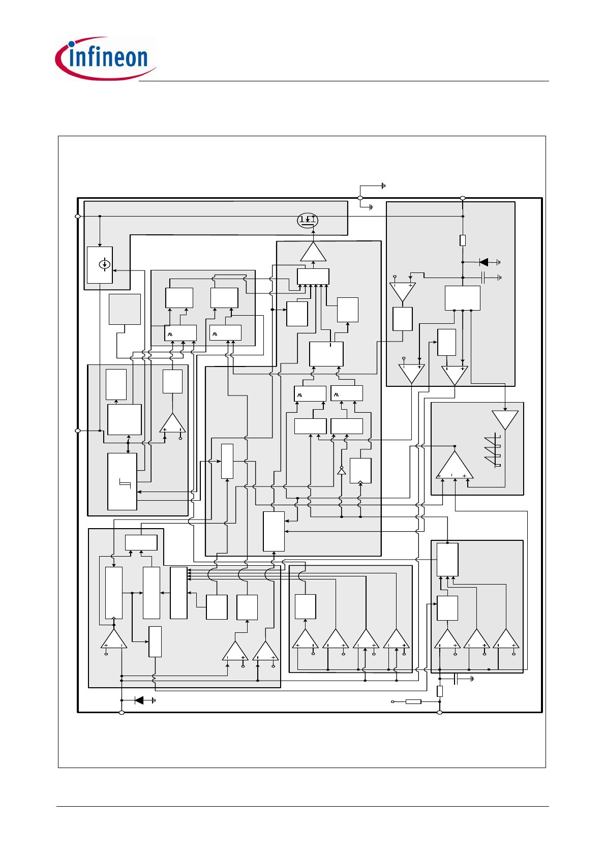
Representative Blockdiagram
Version 2.3
6
November 14, 2012
2
Representative Blockdiagram
Figure 2
Representative Block diagram
1
G2
1
G7
R
SQ
la
tc
hed
P
rot
ec
t
R
SQ
Au
to
re
st
ar
t
Pr
ot
ec
t
P
ro
tect
io
n
R
FB
1
G3
25
kO
2pF
D1
&
G1
&
G5
1
G4
t
BE
B
&
G6
A
ctiv
e B
ur
st B
lo
ck
FB
C8
V
FB
E
B
C9
V
FB
B
O
n
C1
0
V
FB
B
O
ff
C3
V
ZC
R
S
C2
V
ZC
O
V
P
De
la
y
t
ZC
O
V
P
f
sB
OS
C
Ac
tiv
e
Bu
rs
t M
od
e
t
CO
UN
T
C1
V
ZC
C
ZC
U
p/
dow
n c
ount
er
ZC
c
ount
er
cl
k
C
om
par
at
or
So
ft-
st
ar
t
R
ingi
ng
S
uppr
es
si
on
C
oun
t=
7
V
REF
R
S
Q
G8
&
G9
St
ar
tu
p C
el
l
Dr
ai
n
CS
VC
C
Ga
te
Dr
iv
e
G
PW
M
PW
M
O
P
C
urre
nt
M
od
e
PW
M
C
om
par
at
or
V
PW
M
q
V
ol
tage
R
ef
er
enc
e
U
nde
rv
ol
ta
ge
Lo
ck
ou
t
18
V
10.
5
10us
In
te
rn
al
Bi
as
P
ow
er
M
an
age
m
ent
D
epl
. C
ool
M
O
S
®
T
On
M
ax
C7
V
FB
ZL
C6
V
FB
ZH
C5
V
FB
R
1
C4
V
FB
O
LP
t
OL
P
_B
R
egul
at
io
n
C
ur
re
nt L
im
iti
ng
10
kO
D2
Lea
di
ng
E
dge
B
lank
ing
t
LE
B
1p
F
Fo
ld
bac
k
C
orre
ct
io
n
De
la
y
t
CSS
W
C1
3
V
CSB
C1
4
V
CSS
W
C1
5
PW
M
C
ont
ro
l
Ze
ro
C
ros
si
ng
Ga
te
D
ri
ve
r
GN
D
en
C1
2
V
VCCO
V
P
T
O
ffM
ax
OT
P
Version 2.3
7
November 14, 2012
CoolSET
®
- Q1
ICE2QR4765
Functional Description
3
Functional Description
3.1
VCC Pre-Charging and Typical
VCC Voltage During Start-up
In ICE2QR4765, a startup cell is integrated into the
CoolMOS
®
. As shown in Figure 2, the start cell consists
of a high voltage device and a controller, whereby the
high voltage device is controlled by the controller. The
startup cell provides a pre-charging of the VCC
capacitor till VCC voltage reaches the VCC turned-on
threshold V
VCCon
and the IC begins to operate.
Once the mains input voltage is applied, a rectified
voltage shows across the capacitor C
bus
. The high
voltage device provides a current to charge the VCC
capacitor C
vcc
. Before the VCC voltage reaches a
certain value, the amplitude of the current through the
high voltage device is only determined by its channel
resistance and can be as high as several mA. After the
VCC voltage is high enough, the controller controls the
high voltage device so that a constant current around
1mA is provided to charge the VCC capacitor further,
until the VCC voltage exceeds the turned-on threshold
V
VCCon
. As shown as the time phase I in Figure 3, the
VCC voltage increase near linearly and the charging
speed is independent of the mains voltage level.
Figure 3
VCC voltage at start up
The time taking for the VCC pre-charging can then be
approximately calculated as:
[1]
where I
VCCcharge2
is the charging current from the
startup cell which is 1.05mA, typically.
Exceeds the VCC voltage the turned-on threshold
V
VCCon
of at time t
1
, the startup cell is switched off, and
the IC begins to operate with a soft-start. Due to power
consumption of the IC and the fact that still no energy
from the auxiliary winding to charge the VCC capacitor
before the output voltage is built up, the VCC voltage
drops (Phase II). Once the output voltage is high
enough, the VCC capacitor receives then energy from
the auxiliary winding from the time point t
2
on. The VCC
then will reach a constant value depending on output
load.
3.2
Soft-start
At the time t
on
, the IC begins to operate with a soft-start.
By this soft-start the switching stresses for the switch,
diode and transformer are minimised. The soft-start
implemented in ICE2QR4765 is a digital time-based
function. The preset soft-start time is 12ms with 4
steps. If not limited by other functions, the peak voltage
on CS pin will increase step by step from 0.32V to 1V
finally.
Figure 4
Maximum current sense voltage during
softstart
3.3
Normal Operation
The PWM controller during normal operation consists
of a digital signal processing circuit including an up/
down counter, a zero-crossing counter (ZC counter)
and a comparator, and an analog circuit including a
current measurement unit and a comparator. The
switch-on and -off time points are each determined by
the digital circuit and the analog circuit, respectively. As
input information for the switch-on determination, the
zero-crossing input signal and the value of the up/down
counter are needed, while the feedback signal V
FB
and
the current sensing signal V
CS
are necessary for the
switch-off determination. Details about the full
operation of the PWM controller in normal operation
are illustrated in the following paragraphs.
3.3.1
Digital Frequency Reduction
As mentioned above, the digital signal processing
circuit consists of an up/down counter, a ZC counter
and a comparator. These three parts are key to
implement digital frequency reduction with decreasing
load. In addition, a ringing suppression time controller
is implemented to avoid mistriggering by the high
frequency oscillation, when the output voltage is very
low under conditions such as soft start or output short
circuit . Functionality of these parts is described as in
the following.
V
VCCon
V
VCC
V
VCCoff
t1
t
t2
i
ii
iii
t
1
V
VCCon
C
vcc
⋅
I
VCCch
e2
arg
------------------------------------------
=
t
on
3
6
9
12
0.32
0.49
0.66
0.83
1.00
Vcs_sst
(V)
Time(ms)
CoolSET
®
- Q1
ICE2QR4765
Functional Description
Version 2.3
8
November 14, 2012
3.3.1.1
Up/down counter
The up/down counter stores the number of the zero
crossing to be ignored before the main power switch is
switched on after demagnetisation of the transformer.
This value is fixed according to the feedback voltage,
V
FB
, which contains information about the output
power. Indeed, in a typical peak current mode control,
a high output power results in a high feedback voltage,
and a low output power leads to a low regulation
voltage. Hence, according to V
FB
, the value in the up/
down counter is changed to vary the power MOSFET
off-time according to the output power. In the following,
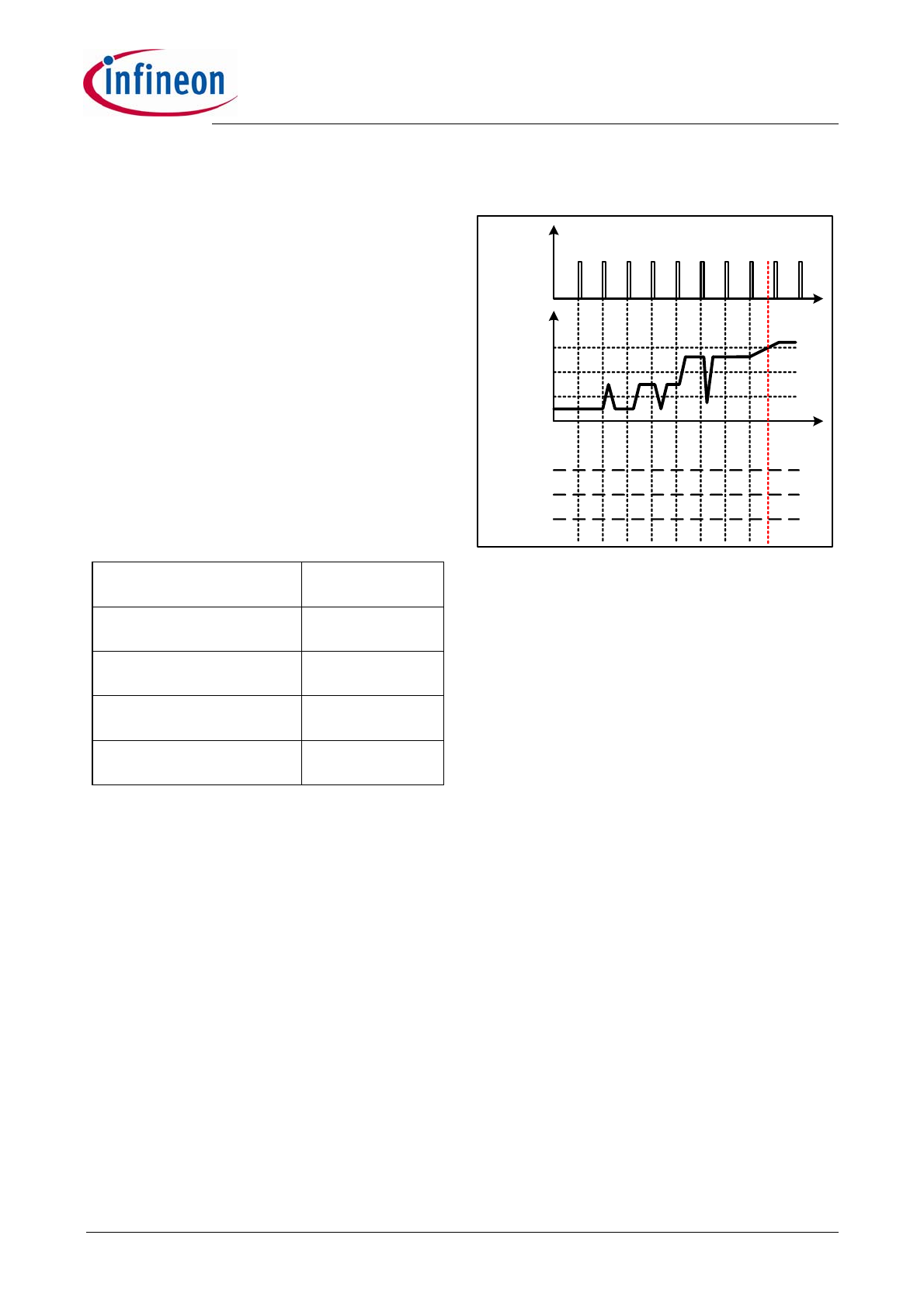
the variation of the up/down counter value according to
the feedback voltage is explained.
The feedback voltage V
FB
is internally compared with
three threshold voltages V
RL
, V
RH
and V
RM
, at each
clock period of 48ms. The up/down counter counts then
upward, keep unchanged or count downward, as
shown in Table 1.
Table 1
Operation of the up/down counter
In the ICE2QR4765, the number of zero crossing is
limited to 7. Therefore, the counter varies between 1
and 7, and any attempt beyond this range is ignored.
When V
FB
exceeds V
FBR1
voltage, the up/down counter
is initialised to 1, in order to allow the system to react
rapidly to a sudden load increase. The up/down
counter value is also intialised to 1 at the start-up, to
ensure an efficient maximum load start up.
Figure 5
shows some examples on how up/down counter is
changed according to the feedback voltage over time.
The use of two different thresholds V
FBZL
and V
FBZH
to
count upward or downward is to prevent frequency
jittereing when the feedback voltage is close to the
threshold point. However, for a stable operation, these
two thresholds must not be affected by the foldback
current limitation (see Section 3.4.1), which limits the
V
CS
voltage. Hence, to prevent such situation, the
threshold voltages, V
FBZL
and V
FBZH
, are changed
internally depending on the line voltage levels.
Figure 5
Up/down counter operation
3.3.1.2
Zero crossing (ZC counter)
In the system, the voltage from the auxiliary winding is
applied to the zero-crossing pin through a RC network,
which provides a time delay to the voltage from the
auxiliary winding. Internally, this pin is connected to a
clamping network, a zero-crossing detector, an output
overvoltage detector and a ringing suppression time
controller.
During on-state of the power switch a negative voltage
applies to the ZC pin. Through the internal clamping
network, the voltage at the pin is clamped to certain
level.
The ZC counter has a minimum value of 0 and
maximum value of 7. After the internal MOSFET is
turned off, every time when the falling voltage ramp of
on ZC pin crosses the 100mV threshold, a zero
crossing is detected and ZC counter will increase by 1.
It is reset every time after the DRIVER output is
changed to high.
The voltage v
ZC
is also used for the output overvoltage
protection. Once the voltage at this pin is higher than
the threshold V
ZCOVP
during off-time of the main switch,
the IC is latched off after a fixed blanking time.
To achieve the switch-on at voltage valley, the voltage
from the auxiliary winding is fed to a time delay network
(the RC network consists of D
zc
, R
zc1
, R
zc2
and C
zc
as
shown in typical application circuit) before it is applied
to the zero-crossing detector through the ZC pin. The
needed time delay to the main oscillation signal
Δt
should be approximately one fourth of the oscillation
period (by transformer primary inductor and drain-
source capacitor) minus the propagation delay from
v
FB
up/down counter
action
Always lower than V
FBZL
Count upwards till
7
Once higher than V
FBZL
, but
always lower than V
FBZH
Stop counting, no
value changing
Once higher than V
FBZH
, but
always lower than V
FBR1
Count downwards
till 1
Once higher than V
FBR1
Set up/down
counter to 1
1
Case 3
Case 2
Case 1
Up/down
counter
n
n+1
n+2
n+2
n+2
n+2
n+1
n
n-1
4 5 6 6 6 6 5 4 3
1
1
2 3 4 4 4 4 3 2 1
7 7 7 7 7 7 6 5 4
t
t
V
FB
V
FBR1
V
FBZH
V
FBZL
clock
T=48ms
1

CoolSET
®
- Q1
ICE2QR4765
Functional Description
Version 2.3
9
November 14, 2012
thedetected zero-crossing to the switch-on of the main
switch t
delay
, theoretically:
[2]
This time delay should be matched by adjusting the
time constant of the RC network which is calculated as:
[3]
3.3.1.3
Ringing suppression time
After MOSFET is turned off, there will be some
oscillation on V
DS
, which will also appear on the voltage
on ZC pin. To avoid that the MOSFET is turned on
mistriggerred by such oscillations, a ringing
suppression timer is implemented. The time is
dependent on the voltage v
ZC
. When the voltage v
ZC
is
lower than the threshold V
ZCRS
, a longer preset time
applies, while a shorter time is set when the voltage v
ZC
is higher than the threshold.
3.3.1.4
Switch on determination
After the gate drive goes to low, it can not be changed
to high during ring suppression time.
After ring suppression time, the gate drive can be
turned on when the ZC counter value is higher or equal
to up/down counter value.
However, it is also possible that the oscillation between
primary inductor and drain-source capacitor damps
very fast and IC can not detect enough zero crossings
and ZC counter value will not be high enough to turn on
the gate drive. In this case, a maximum off time is
implemented. After gate drive has been remained off
for the period of T
OffMax
, the gate drive will be turned on
again regardless of the counter values and V
ZC
. This
function can effectively prevent the switching
frequency from going lower than 20kHz, otherwise
which will cause audible noise, during start up.
3.3.2
Switch Off Determination
In the converter system, the primary current is sensed
by an external shunt resistor, which is connected
between low-side terminal of the main power switch
and the common ground. The sensed voltage across
the shunt resistor v
CS
is applied to an internal current
measurement unit, and its output voltage V
1
is
compared with the regulation voltage V
FB
. Once the
voltage V
1
exceeds the voltage V
FB
, the output flip-flop
is reset. As a result, the main power switch is switched
off. The relationship between the V
1
and the v
CS
is
described by:
[4]
To avoid mistriggering caused by the voltage spike
across the shunt resistor at the turn on of the main
power switch, a leading edge blanking time, t
LEB
, is
applied to the output of the comparator. In other words,
once the gate drive is turned on, the minimum on time
of the gate drive is the leading edge blanking time.
In addition, there is a maximum on time, t
OnMax
,
limitation implemented in the IC. Once the gate drive
has been in high state longer than the maximum on
time, it will be turned off to prevent the switching
frequency from going too low because of long on time.
3.4
Current Limitation
There is a cycle by cycle current limitation realized by
the current limit comparator to provide an overcurrent
detection. The source current of the MOSFET is
sensed via a sense resistor R
CS
. By means of R
CS
the
source current is transformed to a sense voltage V
CS
which is fed into the pin CS. If the voltage V
CS
exceeds
an internal voltage limit, adjusted according to the
Mains voltage, the comparator immediately turns off
the gate drive.
To prevent the Current Limitation process from
distortions caused by leading edge spikes, a Leading
Edge Blanking time (t
LEB
) is integrated in the current
sensing path.
A further comparator is implemented to detect
dangerous current levels (V
CSSW
) which could occur if
one or more transformer windings are shorted or if the
secondary diode is shorted. To avoid an accidental
latch off, a spike blanking time of t
CSSW
is integrated in
the output path of the comparator .
3.4.1
Foldback Point Correction
When the main bus voltage increases, the switch on
time becomes shorter and therefore the operating
frequency is also increased. As a result, for a constant
primary current limit, the maximum possible output
power is increased, which the converter may have not
been designed to support.
To avoid such a situation, the internal foldback point
correction circuit varies the V
CS
voltage limit according
to the bus voltage. This means the V
CS
will be
decreased when the bus voltage increases. To keep a
constant maximum input power of the converter, the
Δt
T
osc
4
------------
t
delay
–
=
τ
td
C
zc
R
zc1
R
zc2
⋅
R
zc1
R
zc2
+
---------------------------------
⋅
=
V
1
3.3 V
cs
⋅
0.7
+
=
CoolSET
®
- Q1
ICE2QR4765
Functional Description
Version 2.3
10
November 14, 2012
required maximum V
CS
versus various input bus
voltage can be calculated, which is shown in
Figure 6
.
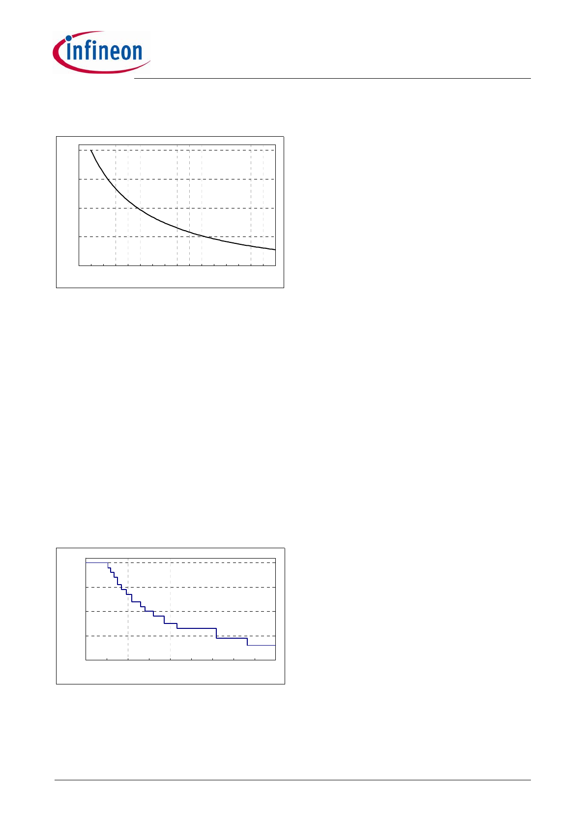
Figure 6
Variation of the VCS limit voltage according
to the IZC current
According to the typical application circuit, when
MOSFET is turned on, a negative voltage proportional
to bus voltage will be coupled to auxiliary winding.
Inside CoolSET
®
-Q1, an internal circuit will clamp the
voltage on ZC pin to nearly 0V. As a result, the current
flowing out from ZC pin can be calculated as
[5]
When this current is higher than I
ZC_1
, the amount of
current exceeding this threshold is used to generate an
offset to decrease the maximum limit on V
CS
. Since the
ideal curve shown in
Figure 6
is a nonlinear one, a
digital block in CoolSET
®
-Q1 is implemented to get a
better control of maximum output power. Additional
advantage to use digital circuit is the production
tolerance is smaller compared to analog solutions. The
typical maximum limit on V
CS
versus the ZC current is
shown in
Figure 7
.
Figure 7
V
CS-max
versus I
ZC
3.5
Active Burst Mode Operation
At light load condition, the IC enters Active Burst Mode
operation to minimize the power consumption. Details
about Active Burst Mode operation are explained in the
following paragraphs.
3.5.1
Entering Active Burst Mode Operation
For determination of entering Active Burst Mode
operation, three conditions apply:
•
the feedback voltage is lower than the threshold of
V
FBEB
(1.25V). Accordingly, the peak current sense
voltage across the shunt resistor is 0.17;
•
the up/down counter is 7; and
•
a certain blanking time (t
BEB
).
Once all of these conditions are fulfilled, the Active
Burst Mode flip-flop is set and the controller enters
Active Burst Mode operation. This multi-condition
determination for entering Active Burst Mode operation
prevents mistriggering of entering Active Burst Mode
operation, so that the controller enters Active Burst
Mode operation only when the output power is really
low during the preset blanking time.
3.5.2
During Active Burst Mode Operation
After entering the Active Burst Mode the feedback
voltage rises as V
OUT
starts to decrease due to the
inactive PWM section. One comparator observes the
feedback signal if the voltage level V
BH
(3.6V) is
exceeded. In that case the internal circuit is again
activated by the internal bias to start with swtiching.
Turn-on of the power MOSFET is triggered by the
timer. The PWM generator for Active Burst Mode
operation composes of a timer with a fixed frequency of
52kHz, typically, and an analog comparator. Turn-off is
resulted by comparison of the voltage signal v
1
with an
internal threshold, by which the voltage across the
shunt resistor V
csB
is 0.34V, accordingly. A turn-off can
also be triggered by the maximal duty ratio controller
which sets the maximal duty ratio to 50%. In operation,
the output flip-flop will be reset by one of these signals
which come first.
If the output load is still low, the feedback signal
decreases as the PWM section is operating. When
feedback signal reaches the low threshold V
BL
(3.0V),
the internal bias is reset again and the PWM section is
disabled until next time regultaion siganl increases
beyond the V
BH
threshold. If working in Active Burst
Mode the feedback signal is changing like a saw tooth
between 3.0V and 3.6V shown in
Figure 8
.
3.5.3
Leaving Active Burst Mode Operation
The feedback voltage immediately increases if there is
a high load jump. This is observed by one comparator.
As the current limit is 34% during Active Burst Mode a
certain load is needed so that feedback voltage can
exceed V
LB
(4.5V). After leaving active busrt mode,
maximum current can now be provided to stabilize V
O
.
In addition, the up/down counter will be set to 1
0.6
0.7
0.8
0.9
1
80
100 120 140 160 180 200 220 240 260 280 300 320 340 360 380 400
Vin(V)
Vc
s
-m
a
x
(V)
I
ZC
V
BUS
N
a
R
ZC1
N
P
------------------------
=
0.6
0.7
0.8
0.9
1
300
500
700
900
1100
1300
1500
1700
1900
2100
Iz c(uA)
Vc
s
-m
a
x
(V)