

I C B 1 F L 0 2 G
S m a r t B a l l a s t C o n t r o l I C f o r
F l u o r e s c e n t L a m p B a l l a s t s
P o w e r M a n a g e m e n t & S u p p l y
D a t a s h e e t V e r s i o n 2 . 1 , S e p t e m b e r 2 0 0 8

Edition 2008-09
Published by
Infineon Technologies AG
81726 Munich, Germany
©
10/16/08 Infineon Technologies AG
All Rights Reserved.
Legal Disclaimer
The information given in this document shall in no event be regarded as a guarantee of conditions or
characteristics. With respect to any examples or hints given herein, any typical values stated herein and/or any
information regarding the application of the device, Infineon Technologies hereby disclaims any and all warranties
and liabilities of any kind, including without limitation, warranties of non-infringement of intellectual property rights
of any third party.
Information
For further information on technology, delivery terms and conditions and prices, please contact the nearest
Infineon Technologies Office (
www.infineon.com
).
Warnings
Due to technical requirements, components may contain dangerous substances. For information on the types in
question, please contact the nearest Infineon Technologies Office.
Infineon Technologies components may be used in life-support devices or systems only with the express written
approval of Infineon Technologies, if a failure of such components can reasonably be expected to cause the failure
of that life-support device or system or to affect the safety or effectiveness of that device or system. Life support
devices or systems are intended to be implanted in the human body or to support and/or maintain and sustain
and/or protect human life. If they fail, it is reasonable to assume that the health of the user or other persons may
be endangered.
ICB1FL02G
Revision History:
2008-09
V 2.1
Previous Version:
2005-06-06 (ICB1FL01G)
Page
Subjects (major changes since last revision)
19
Min Duration of EOL1
25
Preheating Time updated
26
EOL Current Threshold, AC & DC
Previous Version:
2006-02-08 (ICB1FL02G)
3
Package PG-DSO-18-2, halogen-free mould compound, WEEE compliant
11
Function removed and sentence deleted “During ignition and prerun mode the notch filter is
bypassed.”
18
State diagram reworked (frequency range description corrected)
23
PFC zero current detector: clamping of positive voltages
24
PFC section: initial on-time and repetition time adapted
25
Inverter control: minimum duration of fault conditions EOL1, Cap Load 2 adapted
26
Restart after lamp removal: discharge resistor value adapted
33
L
C
equations corrected
Type
Package
ICB1FL02G
PG-DSO-18-2
ICB1FL02G
PG-DSO-18-1
Datasheet Version 2.1
3
September 2008
Product Highlights
• Lowest Count of external Components
• HV-Driver with coreless Transformer Technology
• Improved Reliability and minimized Spread due to
digital and optimized analog control functions
Features PFC
•
Discontinuous Conduction Mode PFC
•
Integrated Compensation of PFC Control Loop
•
Adjustable PFC Current Limitation
•
Adjustable PFC Bus Voltage
Features Lamp Ballast Inverter
•
Supports Restart after Lamp Removal and End-of-
Life Detection in Multi-Lamp Topologies
•
End-of-Life (EOL) detected by adjustable
± Thresholds of sensed lamp voltage
•
Rectifier Effect detected by ratio of ± Amplitude of
Lamp Voltage
•
Detection of different capacitive Mode Operations
•
Adjustable Inverter Overcurrent Shutdown
•
Self-adaption of Ignition Time from 40ms to 235ms
•
Parameters adjustable by Resistors only
•
Pb-free lead plating; RoHS compliant
•
Halogen-free mould compound, WEEE compliant
Smart Ballast Control IC for
Fluorescent Lamp Ballasts
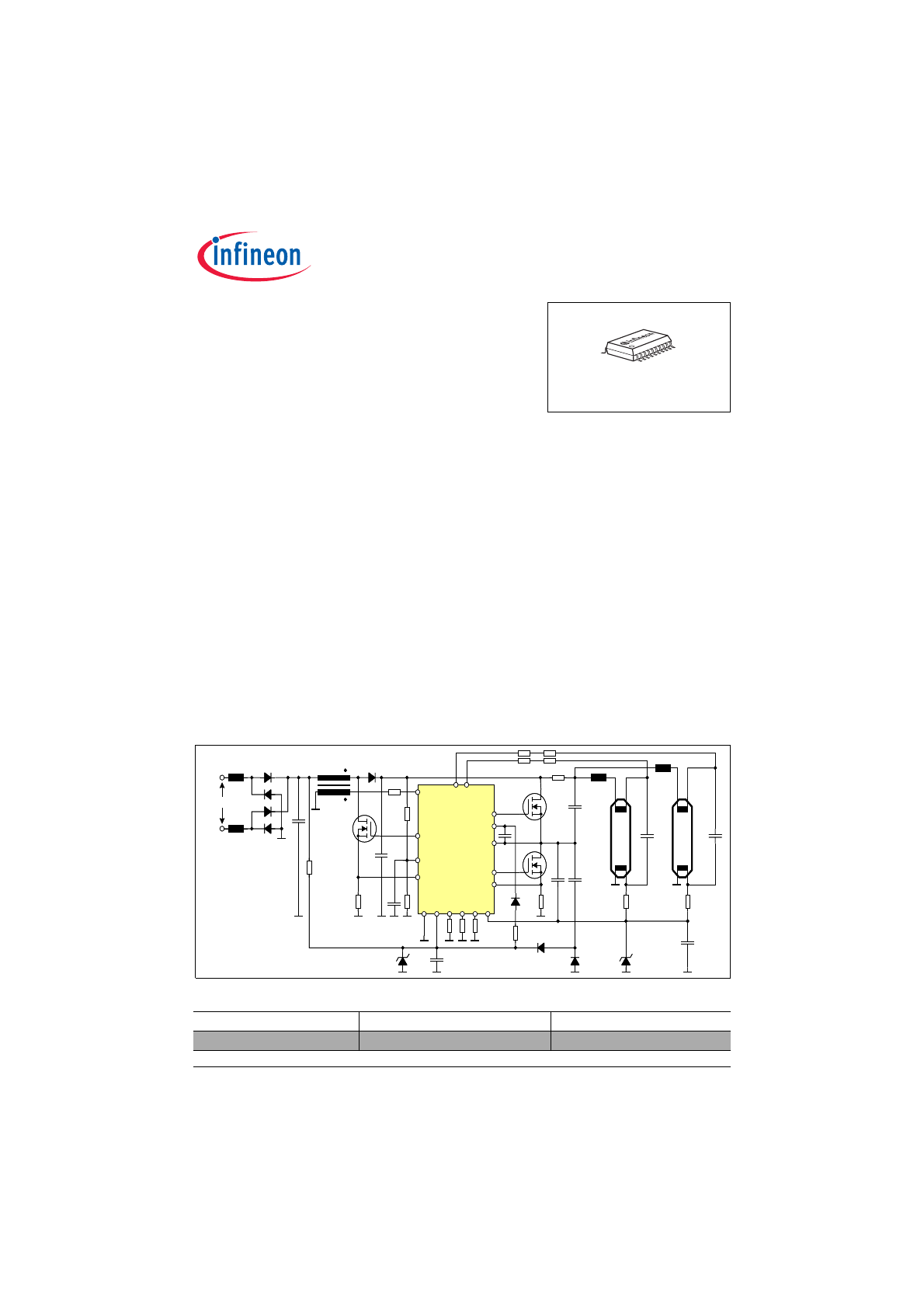
Description
The Smart Ballast IC is designed to control a Fluorescent
Lamp Ballast including a Discontinuous Conduction
Mode Power Factor Correction (PFC), a lamp Inverter
Control and a High Voltage Level Shift Half-Bridge
Driver.
The application requires a minimum of external
components. There are integrated low pass filters and an
internal compensation for the PFC voltage loop control.
Preheating time is adjustable by a single resistor only in
the range between 0 and 2000ms. In the same way the
preheating frequency and run frequency are set by
resistors only. The control concept covers requirements
for T5 lamp ballasts such as detection of end-of-life and
detection of capacitive mode operation and other
protection measures even in multilamp topologies.
ICB1FL02G is easy to use and easy to design and
therefore a basis for a cost effective solution for
fluorescent lamp ballasts.
RF
RU
N
RF
P
H
RT
P
H
VC
C
PFCZCD
PFCGD
PFCVS
PFCCS
HSGD
HSVCC
HSGND
LSGD
LSCS
LV
S
2
LV
S
1
RE
S
GN
D
90 ... 270 V AC
ICB1
F
L
0
2
G
RF
RU
N
RF
P
H
RT
P
H
VC
C
PFCZCD
PFCGD
PFCVS
PFCCS
HSGD
HSVCC
HSGND
LSGD
LSCS
LV
S
2
LV
S
1
RE
S
GN
D
90 ... 270 V AC
ICB1
F
L
0
2
G
PG-DSO-18-2

ICB1FL02G
Table of Contents
Page
Datasheet Version 2.1
4
September 2008
1
Pin Configuration and Description . . . . . . . . . . . . . . . . . . . . . . . . . . . . . .5
1.1
Pin Configuration PG-DSO-18-1 . . . . . . . . . . . . . . . . . . . . . . . . . . . . . . . . . .5
1.2
Pin Description . . . . . . . . . . . . . . . . . . . . . . . . . . . . . . . . . . . . . . . . . . . . . . . .5
2
Block Diagram . . . . . . . . . . . . . . . . . . . . . . . . . . . . . . . . . . . . . . . . . . . . . . .8
3
Functional Description . . . . . . . . . . . . . . . . . . . . . . . . . . . . . . . . . . . . . . . .9
3.1
Typical operating levels during start-up . . . . . . . . . . . . . . . . . . . . . . . . . . . . .9
3.2
PFC Preconverter . . . . . . . . . . . . . . . . . . . . . . . . . . . . . . . . . . . . . . . . . . . .11
3.3
Typical operating levels during start-up . . . . . . . . . . . . . . . . . . . . . . . . . . . .13
3.4
Detection of End-of-Life and Rectifier Effect . . . . . . . . . . . . . . . . . . . . . . . .14
3.5
Detection of capacitive mode operating conditions . . . . . . . . . . . . . . . . . . .15
3.6
Interruption of Operation and Restart after Lamp Removal . . . . . . . . . . . . .16
4
State Diagram . . . . . . . . . . . . . . . . . . . . . . . . . . . . . . . . . . . . . . . . . . . . . . .18
5
Protection Functions . . . . . . . . . . . . . . . . . . . . . . . . . . . . . . . . . . . . . . . . .19
6
Electrical Characteristics . . . . . . . . . . . . . . . . . . . . . . . . . . . . . . . . . . . . .20
6.1
Absolute Maximum Ratings . . . . . . . . . . . . . . . . . . . . . . . . . . . . . . . . . . . . .20
6.2
Operating Range . . . . . . . . . . . . . . . . . . . . . . . . . . . . . . . . . . . . . . . . . . . . .21
6.3
Characteristics . . . . . . . . . . . . . . . . . . . . . . . . . . . . . . . . . . . . . . . . . . . . . . .22
6.3.1
Power Supply Section . . . . . . . . . . . . . . . . . . . . . . . . . . . . . . . . . . . . . . .22
6.3.2
PFC Section . . . . . . . . . . . . . . . . . . . . . . . . . . . . . . . . . . . . . . . . . . . . . . .23
6.3.2.1
PFC Current Sense (PFCCS) . . . . . . . . . . . . . . . . . . . . . . . . . . . . . . .23
6.3.2.2
PFC Zero Current Detector (PFCZCD) . . . . . . . . . . . . . . . . . . . . . . . .23
6.3.2.3
PFC Bus Voltage Sense (PFCVS) . . . . . . . . . . . . . . . . . . . . . . . . . . . .23
6.3.2.4
PFC PWM Generation . . . . . . . . . . . . . . . . . . . . . . . . . . . . . . . . . . . . .24
6.3.2.5
PFC Gate Drive (PFCGD) . . . . . . . . . . . . . . . . . . . . . . . . . . . . . . . . . .24
6.3.3
Inverter Section . . . . . . . . . . . . . . . . . . . . . . . . . . . . . . . . . . . . . . . . . . . .25
6.3.3.1
Inverter Control (RFRUN, RFPH, RTPH) . . . . . . . . . . . . . . . . . . . . . .25
6.3.3.2
Inverter Low Side Current Sense (LSCS) . . . . . . . . . . . . . . . . . . . . . .25
6.3.3.3
Restart after Lamp Removal (RES) . . . . . . . . . . . . . . . . . . . . . . . . . . .26
6.3.3.4
Lamp Voltage Sense (LVS1, LVS2) . . . . . . . . . . . . . . . . . . . . . . . . . .26
6.3.3.5
Inverter Low Side Gate Drive (LSGD) . . . . . . . . . . . . . . . . . . . . . . . . .27
6.3.3.6
Inverter High Side Gate Drive (HSGD) . . . . . . . . . . . . . . . . . . . . . . . .28
7
Application Examples . . . . . . . . . . . . . . . . . . . . . . . . . . . . . . . . . . . . . . . .29
7.1
Operating Behaviour of a Ballast for a single Fluorescent Lamp . . . . . . . . .29
7.2
Design Equations of a Ballast Application . . . . . . . . . . . . . . . . . . . . . . . . . .30
7.3
Multilamp Ballast Topologies . . . . . . . . . . . . . . . . . . . . . . . . . . . . . . . . . . . .35
8
Package Outlines . . . . . . . . . . . . . . . . . . . . . . . . . . . . . . . . . . . . . . . . . . . .36
Datasheet Version 2.1
5
September 2008
ICB1FL02G
Pin Configuration and Description
1
Pin Configuration and Description
1.1
Pin Configuration PG-DSO-18-1
1.2
Pin Description
LSCS (Low side current sense, Pin 1)
This pin is directly connected to the shunt resistor
which is located between the Source terminal of the
low-side MOSFET of the inverter and ground.
Internal clamping structures and filtering measures
allow for sensing the Source current of the low-side
inverter MOSFET without additional filter components.
There is a first threshold of 0,8V, which provides a
couple of increasing steps of frequency during ignition
mode, if exceeded by the sensed current signal for a
time longer than 250ns. If the sensed current signal
exceeds a second threshold of 1,6V for longer than
400ns during all operating modes, a latched shut down
of the IC will be the result.
LSGD (Low side gate drive, Pin 2)
The Gate of the low-side MOSFET in a half-bridge
inverter topology is controlled by this pin. There is an
active L-level during UVLO (undervoltage lockout) and
a limitation of the max. H-level at 11V during normal
operation. Turning on the MOSFET softly (with reduced
di
DRAIN
/dt), the Gate drive voltage rises within 220ns
from L-level to H-level. The fall time of the Gate drive
voltage is less than 50ns in order to turn off quickly.
This measure produces different switching speeds
during turn-on and turn-off as it is usually achieved with
a diode in parallel to a resistor in the Gate drive loop. It
is recommended to use a resistor of about 15Ohm
between drive pin and Gate in order to avoid
oscillations and in order to shift the power dissipation of
discharging the Gate capacitance into this resistor. The
dead time between LSGD signal and HSGD signal is
1800ns typically.
VCC (Supply voltage, Pin 3)
This pin provides the power supply of the ground
related section of the IC. There is a turn-on threshold at
14V and an UVLO threshold at 10,5V. Upper supply
voltage level is 17,5V. There is an internal zener diode
clamping Vcc at 16V (2mA typically). The zener current
is internally limited to 5mA max. For higher current
levels an external zener diode is required. Current
consumption during UVLO and during fault mode is
less than 150
µA. A ceramic capacitor close to the
supply and GND pin is required in order to act as a low-
impedance power source for Gate drive and logic
signal currents.
GND (Ground, Pin 4)
This pin is connected to ground and represents the
ground level of the IC for supply voltage, Gate drive
and sense signals.
Pin
Symbol
Function
1
LSCS
Low side current sense (inverter)
2
LSGD
Low side gate drive (inverter)
3
VCC
Supply voltage
4
GND
Controller ground
5
PFCGD
PFC gate drive
6
PFCCS
PFC current sense
7
PFCZCD PFC zero current detector
8
PFCVS
PFC voltage sense
9
RFRUN
Set R for run frequency
10
RFPH
Set R for preheating frequency
11
RTPH
Set R for preheating time
12
RES
Restart after lamp removal
13
LVS1
Lamp voltage sense 1
14
LVS2
Lamp voltage sense 2
15
n.e.
Not existing
16
n.e.
Not existing
17
HSGND
High side ground
18
HSVCC
High side supply voltage
19
HSGD
High side gate drive
20
HSGND
High side ground
HSVCC
HSGND
RFPH
RES
LVS1
PG-DSO-18-2 (300mil)
LVS2
RFRUN
PFCVS
PFCZCD
IC
B
1
F
L02
G
GND
HSGD
LSGD
PFCGD
LSCS
PFCCS
VCC
RTPH
HSGND
10
9
8
7
4
2
5
1
6
3
11
12
13
14
17
19
16
20
15
18

ICB1FL02G
Pin Configuration and Description
Datasheet Version 2.1
6
September 2008
PFCGD (PFC gate drive, Pin 5)
The Gate of the MOSFET in the PFC preconverter
designed in boost topology is controlled by this pin.
There is an active L-level during UVLO and a limitation
of the max. H-level at 11V during normal operation.
Turning on the MOSFET softly (with a reduced di
DRAIN
/
dt), the Gate drive voltage rises within 220ns from L-
level to H-level. The fall time of the Gate voltage is less
than 50ns in order to turn off quickly. A resistor of about
10Ohm between drive pin and Gate in order to avoid
oscillations and in order to shift the power dissipation of
discharging the Gate capacitance into this resistor is
recommended.
The PFC section of the IC controls a boost converter as
a PFC preconverter in discontinuous conduction mode
(DCM). Typically the control starts with Gate drive
pulses with an on-time of 1
µs increasing up to 24µs and
a off-time of 40
µs. As soon as a sufficient ZCD (zero
current detector) signal is available, the operating
mode changes from a fixed frequent operation to an
operation with variable frequency. During rated and
medium load conditions we get an operation with
critical conduction mode (CritCM), that means
triangular shaped currents in the boost converter choke
without gaps when reaching the zero level and variable
operating frequency. During light load (detected by the
internal error amplifier) we get an operation with
discontinuous conduction mode (DCM), that means
triangular shaped currents in the boost converter choke
with gaps when reaching the zero level and variable
operating frequency in order to avoid steps in the
consumed line current.
PFCCS (PFC current sense, Pin 6)
The voltage drop across a shunt resistor located
between Source of the PFC MOSFET and GND is
sensed with this pin. If the level exceeds a threshold of
1V for longer than 260ns the PFC Gate drive is turned
off as long as the ZCD (zero current detector) enables
a new cycle. If there is no ZCD signal available within
40µs after turn-off of the PFC Gate drive, a new cycle
is initiated from an internal start-up timer.
PFCZCD (PFC zero current detection, Pin 7)
This pin senses the point of time when the current
through the boost inductor becomes zero during off-
time of the PFC MOSFET in order to initiate a new
cycle. The moment of interest appears when the
voltage of the separate ZCD winding changes from
positive to negative level which represents a voltage of
zero at the inductor windings and therefore the end of
current flow from lower input voltage level to higher
output voltage level. There is a threshold with
hysteresis, for increasing voltage a level of 1,5V, for
decreasing voltage a level of 0,5V, that detects the
change of inductor voltage. A resistor connected
between ZCD winding and sense input limits the sink
and source current of the sense pin, when the voltage
of the ZCD winding exceeds the internal clamping
levels (6,3V and -2,9V @ 4mA) of the IC.
If the sensed level of the ZCD winding is not sufficient
(e.g. during start-up), an internal start-up timer will
initiate a new cycle every 40
µs after turn-off of the PFC
Gate drive.
PFCVS (PFC voltage sense, Pin 8)
The intermediate circuit voltage (bus voltage) at the
smoothing capacitor is sensed by a resistive divider at
this pin. The internal reference voltage for rated bus
voltage is 2,5V. There are further thresholds at 0,375V
(15% of rated bus voltage), 1,83V (73% of rated bus
voltage) and 2,725V (109% of rated bus voltage) for
detecting open control loop, undervoltage and
overvoltage.
RFRUN (Set R for run frequency, Pin 9)
A resistor from this pin to ground sets the operating
frequency of the inverter during run mode. Typical run
frequency range is 20kHz to 100kHz. The set resistor
R
RFRUN
can be calculated based on the run frequency
f
RUN
according to the equation
RFPH (Set R for preheating frequency, Pin 10)
A resistor from this pin to ground sets together with the
resistor at pin 9 the operating frequency of the inverter
during preheat mode. Typical preheat frequency range
is run frequency (as a minimum) to 150kHz. The set
resistor R
RFPH
can be calculated based on the preheat
frequency f
PH
and the resistor R
RFRUN
according to the
equation:
The total value of both resistors R
RFPH
and R
RFRUN
switched in parallel should not be less than 3,3kOhm.
RTPH (Set R for preheating time, Pin 11)
A resistor from this pin to ground sets the preheating
time of the inverter during preheat mode. A set resistor
range from zero to 18kOhm corresponds to a range of
preheating time from zero to 2000ms subdivided in 127
steps.
RES (Restart after lamp removal, Pin 12)
A source current out of this pin via resistor and filament
to ground monitors the existence of the low-side
filament of the fluorescent lamp for restart after lamp
R
R FRUN
5 10
8ΩHz
⋅
f
RUN
-----------------------------
=
R
RFPH
R
RFRUN
f
PH
R
R FRUN
⋅
5 10
8ΩHz
⋅
----------------------------------------
1
–
--------------------------------------------------
=

ICB1FL02G
Pin Configuration and Description
Datasheet Version 2.1
7
September 2008
removal. A capacitor from this pin directly to ground
eliminates a superimposed AC voltage that is
generated as a voltage drop across the low-side
filament. With a second sense resistor the filament of a
paralleled lamp can be included into the lamp removal
sense.
During typical start-up with connected filaments of the
lamp a current source I
RES3
(20µA) is active as long as
Vcc> 10,5V and V
RES
< V
RESC1
(1,6V). An open Low-
side filament is detected, when V
RES
> V
RESC1
. Such a
condition will prevent the start-up of the IC. In addition
the comparator threshold is set to V
RESC2
(1,3V) and
the current source changes to I
RES4
(17µA). Now the
system is waiting for a voltage level lower than V
RESC2
at the RES-Pin that indicates a connected low-side
filament, which will enable the start-up of the IC.
An open high-side filament is detected when there is no
sink current I
LVSsink
(15µA) into both of the LVS-Pins
before the V
CC
start-up threshold is reached. Under
these conditions the current source at the RES-Pin is
I
RES1
(41µA) as long as Vcc> 10,5V and V
RES
< V
RESC1
(1,6V) and the current source is I
RES2
(34µA) when the
threshold has changed to V
RESC2
(1,3V). In this way the
detection of the high-side filament is mirrored to the
levels on the RES-Pin.
Finally there is a delay function implemented at the
RES-Pin. When a fault condition happens e.g. by an
end-of-life criteria the inverter is turned-off. In some
topologies a transient AC lamp voltage may occur
immediately after shut down of the Gate drives which
could be interpreted as a lamp removal. In order to
generate a delay for the detection of a lamp removal
the capacitor at the RES-Pin is charged by the I
RES3
(20µA) current source up to the threshold V
RESC1
(1,6V)
and discharged by an internal resistor R
RESdisch
, which
operates in parallel to the external sense resistor at this
pin, to the threshold V
RESC3
(0,375V). The total delay
amounts to 32 of these cycles, which corresponds to a
delay time between 30ms to 100ms dependent on
capacitor value.
In addition this pin is applied to sense capacitive mode
operation by use of a further capacitor connected from
this pin to the nod of the high-side MOSFET’s Source
terminal and the low-side MOSFET’s Drain terminal.
The sense capacitor and the filter capacitor are acting
as a capacitive voltage divider that allows for detecting
voltage slopes versus timing sequence and therefore
indicating capacitive mode operation. A typical ratio of
the capacitive divider is 410V/2,2V which results in the
capacitor values e.g. of 10nF and 53pF (56pF).
LVS1 (Lamp voltage sense 1, Pin 13)
Before the IC enters the softstart mode this pin has to
sense a sink current above 26
µA (max) which is fed via
resistors from the bus voltage across the high-side
filament of the fluorescent lamp in order to monitor the
existence of the filament for restart after lamp removal.
Together with LVS2 (pin 14) and RES (pin 12) the IC
can monitor the lamp removal of totally 4 lamps.
During run mode the lamp voltage is sensed by the AC
current fed into this pin via resistors. Exceeding one of
the two thresholds of either +215
µA or -215µA cycle by
cycle for longer than 610µs, the interpretation of this
event is a failure due to EOL1 (end-of-life). A rectifier
effect (EOL2) is assumed if the ratio of the sequence of
positive and negative amplitudes is above 1,15 or
below 0,85 for longer than 500ms. A failure due to
EOL1 or EOL2 changes the operating mode from run
mode into a latched fault mode that stops the operation
until a reset occurs by lamp removal or by cycle of
power.
EOL1 and EOL2 require an AC current with
zerocrossings at LVS-Pin for a reliable detection. A DC
current at LVS-Pin results in a definite turn-off action
acc. to EOL1 only if the sensed current exceeds the
threshold I
LVSEOLDC
= +/-175µA (typically).
If the functionality of this pin is not required (e.g. for
single lamp designs) it can be disabled by connecting
this pin to ground.
LVS2 (Lamp voltage sense 2, Pin 14)
Same functionality as LVS1 (pin 13) for monitoring a
paralleled lamp circuit.
HSGND (High side ground, Pin 17)
This pin is connected to the Source terminal of the
high-side MOSFET, which is also the nod of high-side
and low-side MOSFET. This pin represents the floating
ground level of the high-side driver and high-side
supply.
HSVCC (High side supply voltage, Pin 18)
This pin provides the power supply of the high-side
ground related section of the IC. An external capacitor
between pin 15 and 16 acts like a floating battery which
has to be recharged cycle by cycle via high voltage
diode from low-side supply voltage during on-time of
the low-side MOSFET. There is an UVLO threshold
with hysteresis that enables high-side section at 10,1V
and disables it at 8,4V.
HSGD (High side gate drive, Pin 19)
The Gate of the high-side MOSFET in a half-bridge
inverter topology is controlled by this pin. There is an
active L-level during UVLO and a limitation of the max.
H-level at 11V during normal operation. The switching
characteristics are the same as described for LSGD
(pin 2). It is recommended to use a resistor of about
15Ohm between drive pin and Gate in order to avoid
oscillations and in order to shift the power dissipation of
discharging the Gate capacitance into this resistor.
The dead time between LSGD signal and HSGD signal
is 1800ns typically.
HSGND (High side ground, Pin 20)
This pin is internally connected with pin 17.
ICB1FL02G
Block Diagram
Datasheet Version 2.1
8
September 2008
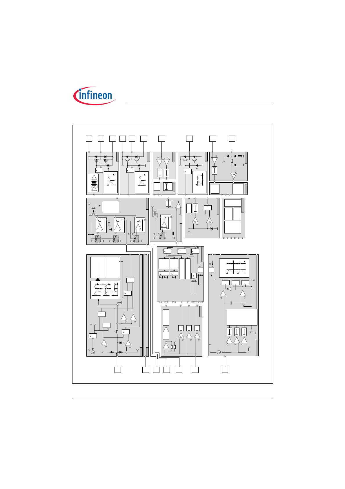
2
Block Diagram
Figure 1
Simplified Blockdiagram of ICB1FL02G
9
RFRUN
8
PFCVS
10
RFPH
11
RTPH
In
t.
S
u
p
p
ly
&
G3
Z1
16
V
@2
m
A
VC
C
5V
5µ
s
B
lank
UV
LO
V
TH
1
=1
4
,0
V
V
TH
2
=1
0
,5
V
C2
V
TH
=
10,
5V
OF
F_
H
V
DD_
goo
d_
H
C1
PO
W
E
R
S
U
PPL
Y
S1
R1
RT
P
H
C1
T1
T2
PH
E
N
D
_
H
5,
0
V
d
ac7
2,
0
V
S
o
ft
s
tar
t and
P
reh
eat
M
ode
O
the
r M
o
des
OP
B
ia
s
C
e
ll1
5µ
s
Bl
a
n
k
PR
EH
E
A
T
_
T
IM
E
R
O
s
ci
lla
to
r
I
os
c
!
f
os
c
S3
S1
R1
OS
C
vref
RF
P
H
RF
R
U
N
T1
T2
I
OS
C
2,
5
V
P
re
heat
M
o
d
e
O
the
r M
odes
O
ther
M
ode
s
R
u
n
M
ode
dac
7
, dac
4
=
G
N
D
du
ri
ng
ru
n
m
ode
,
ot
her
w
is
e
tr
ans
ien
t
v
o
ltage le
v
e
ls
(0
..2
,5
V
)
5,
0
V
da
c
7
da
c
4
VC
O
2,
5
V
da
c
7
OP
B
ia
s
C
e
ll1
OP
B
ia
s
C
e
ll2
OP
B
ia
s
C
e
ll3
S2
VCC
OP
1
R1
A
v
= 2
.5
R2
V
REF
= 2
,5
0
V
8
-Bit
AD
C
C1
V
TH
1
=
2
,72
5V
V
TH
2
=
2
,62
5V
C2
V
TH
=
1,
83V
C3
V
TH
=
0,
375V
VB
U
S
O
V
E
R
VO
L
T
AG
E
VB
U
S
UNDE
RV
O
L
T
A
G
E
VB
U
S
O
PEN
LO
O
P
DE
T
E
CT
D
IGI
T
A
L
L
OOP
CO
NT
RO
L
PF
C
_
P
W
M
_
IN
5µ
s
Bl
a
n
k
5µ
s
Bl
a
n
k
5µ
s
Bl
a
n
k
PF
C
_
V
S
EN
D
-O
F
-L
IF
E 2
LV
S
2
14
LVS2
LV
S
_
2
SPI
fo
r
Test
M
ode
Bandga
p
Vr
ef
=
2
.5
V
Ma
st
e
r
Cl
ock
Di
gi
ta
l
sequen
ti
al
cont
ro
l
da
c
4
da
c
7
DS
C
OS
C
PH
EN
D
_
H
M
C
L
O
C
K
_
SPI
P
O
WE
R
_
D
O
WN
_
L
D1
PF
C
C
S
C1
1.
0V
26
0ns
B
lank
C2
V
TH
1
=1
,5
V
V
TH
2
=0
,5
V
D2
R1
R2
D3
5,
0
V
PF
C
_
Z
C
D
PF
C
_
C
L
IM
6
PFCC
S
7
PFCZCD
D1
S
tar
t-
up
tim
e
r
o
ff-
ti
m
e
40
µ
s
PF
C
PW
M
&
Co
nt
ro
l
PF
C
P
W
M
PF
C
_
PW
M
_
IN
PF
C
G
D
IN
DS
C
PF
C
G
D
Z1
1
G1
T2
T1
D2
D1
VC
C
PF
C
G
D
IN
5
PFCG
D
sl
o
pe c
ont
ro
l
Z1
=
12V
0
220
ns
t
V
GA
T
E
1,
8µ
s
D
ead
ti
m
e
PW
M
inv
e
rt
er
IN
VPW
M
DS
C
LS
HS
C1
C2
0,
8V
1,
6V
2
50n
s
Bl
a
n
k
4
00n
s
Bl
a
n
k
IN
V
_
O
C
IG
N
-L
IM
INV
C
L
IM
1
LSCS
2
LSGD
3
4
GN
D
LS
G
D
Z1
1
G1
T2
T1
D2
D1
VC
C
LS
s
lope c
ont
ro
l
Z1
=
12V
0
2
2
0ns
t
V
GA
T
E
HS
G
D
Z1
1
G1
D2
D1
T1
T2
HSVCC
19
18
17
HS
GD
HSG
N
D
sl
o
pe c
ont
ro
l
Z1
=
12V
0
2
2
0ns
t
V
GA
T
E
HS
Cor
e
le
ss
T
.
&
G6
C3
C4
D2
D1
VC
C
5V
EN
D
-O
F
-L
IF
E
1
DQ
&
G2
EN
I1
= 5
µ
A
P
O
W
E
R_
DO
W
N
_
L
H =
on
L =
of
f
EO
L
O
F
F
_
L
EO
L
A
C
T
IVE_
H
LI
NS
E
R
T
_
H
G3
E
N
=L
=>
S
ta
tu
s
L
a
tc
h
e
d
+
215µ
A
-2
15µ
A
1
G5
C1
15µ
A
C2
2,
0V
D3
1
G1
1
G4
I
LV
S
L
VS1
13
LVS1
> 1
,1
5
....
..
...
=>
Q
=
H
=
0,
8
5
..
1,
15=
>
Q
=
L
< 0
,8
5
…
...
..
=
>
Q
= H
Q
OFF_
H
V
P
EAK
(N
+1
)
V
P
EAK
(N
)
=
LV
S
_
1
T1
N
I
LV
S
P
e
a
k
R
e
c
tif
ic
a
tio
n
N+
2
N+
1
V
PE
AK
(N
+
1
)
V
PE
AK
(N
)
E
ND-
O
F
-L
IF
E
2
C
APAC
IT
IVE L
O
AD
1
OP
E
N
FI
L
A
M
E
N
T
VBU
S O
V
ER
VO
L
T
AG
E
IN
VER
T
E
R
O
V
E
RCURRE
NT
Up &
Dow
n
Cou
n
te
r
m
in.
du
ra
ti
on
o
f e
ffe
c
t:
50
0m
s
E
ND-
O
F
-L
IF
E
1
C
APAC
IT
IVE L
O
AD
2
O
P
ER
AT
IO
N
ABO
VE
RUN F
R
E
Q
UE
NCY
1
E
RRO
R_L
O
G
IC
m
in.
d
u
ra
ti
o
n
of
ef
fe
c
t:
40
0n
s
m
in
.dur
at
io
n
of
ef
fe
c
t:
6
10µ
s
23
5m
s
a
ft
e
r en
d of
pr
eh
eat
m
o
d
e
1
R
S
Q
Q
FA
UL
T
LA
T
C
H
1
P
O
WE
R
_
D
O
WN
_
L
L
VS1
_
L
L
VS2
_
L
O
FF_
H
LA
M
P
_I
NS
E
R
T
_
H
UV
L
O
_L
O
P
E
N
_L
O
O
P
_L
&
1
1
0,
3
75V
1,
3V
1,
6V
5,
0
V
T1
3,
2
V
0,
2
4
V
IN
V
1
T1
D
Q
D
Q
G1
D
Q
G2
G3
12
RES
5µ
s
Bl
a
n
k
5µ
s
Bl
a
n
k
5µ
s
Bl
a
n
k
I3
= 2
0
µ
A
;
V
RE
S
<
1,
6V
;
V
CC
>
10,
5V
;
I
LV
S
>
15µ
A
; or
du
ri
ng r
u
n
m
o
d
e
I1
= 4
1
µ
A
;
V
RE
S
<
1,
6V
;
V
CC
>
10,
5V
;
I
LV
S
<
15µ
A
;
I4
= 1
7
µ
A
;
V
RE
S
>
1,
6V
;
V
CC
>
10,
5V
;
I
LV
S
>
15µ
A
;
I2
= 3
4
µ
A
;
V
RE
S
>
1,
6V
;
V
CC
>
10,
5V
;
I
LV
S
<
15µ
A
;
I5
=
4
1
µ
A
&
0
µ
A
al
te
rnat
ing
fo
r 3
2
c
y
c
les
as
a
del
ay
;
V
DS
C
apa
c
it
iv
e
Loa
d
De
te
c
tio
n
C
AP L
O
AD
1
V
DS
C
AP L
O
AD
2
CA
P
L
O
A
D-
RE
S
Lam
p i
n
s
e
rt
det
ec
tion f
o
r
VR
ES <
1
,6
V
dur
in
g
pow
e
r dow
n.
D
e
la
y
gen
er
at
or
fo
r a
c
tiv
a
ti
n
g
la
mp
r
e
mo
v
a
l
a
fte
r fa
u
lt
l
a
tc
h
is
s
e
t.
LS
G
D
IN
_H
HS
G
D
IN
_H
C
APL
O
A
D
1
C
APL
O
A
D
2
O
P
EN
_
F
IL
AM
EN
T
L
VS2
L
VS1
LA
M
P
_
IN
S
E
R
T
_
H
&
C1
C4
C3
C5
C2
54
k
ICB1FL02G
Functional Description
Datasheet Version 2.1
9
September 2008
3
Functional Description
3.1
Typical operating levels during start-up
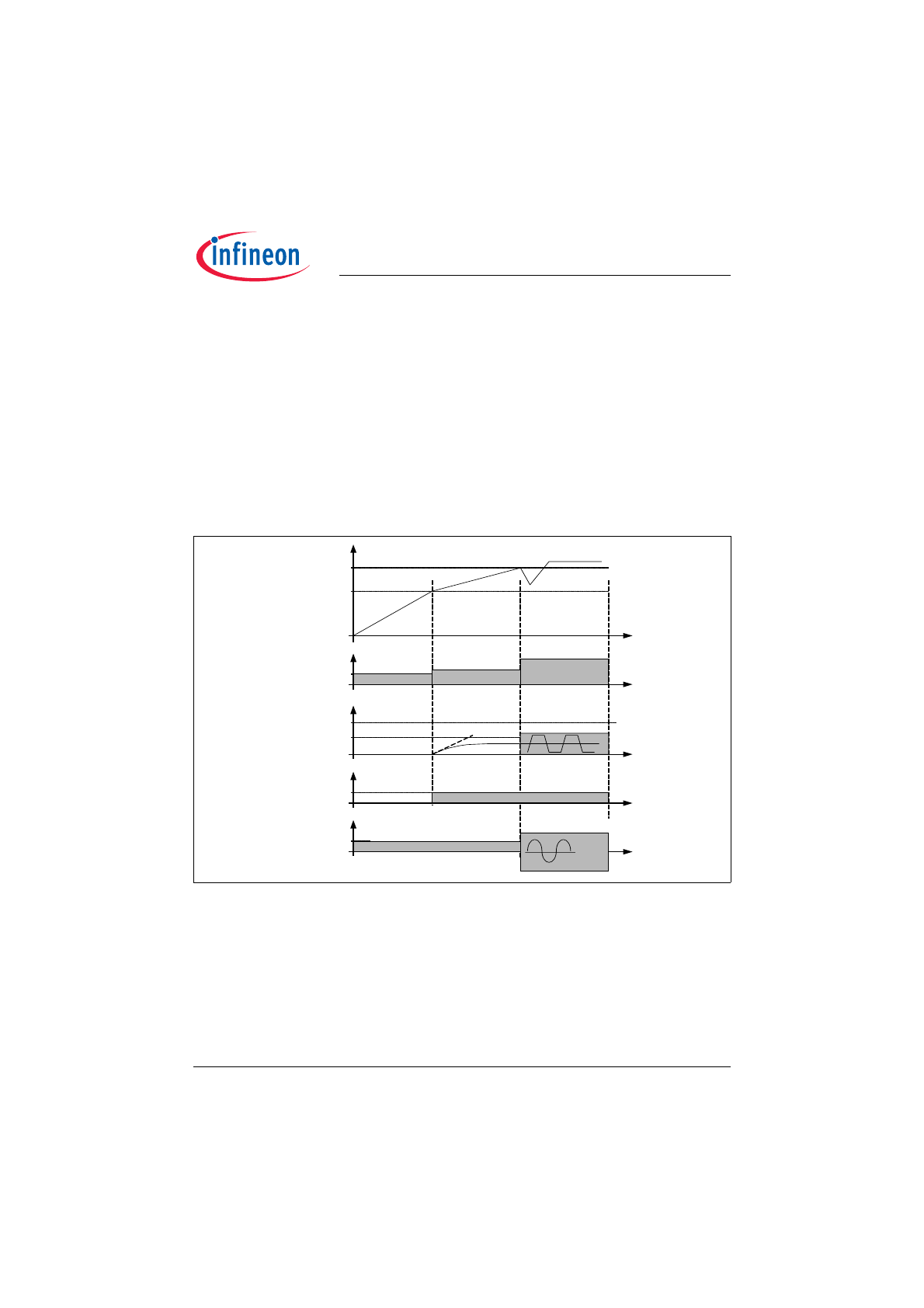
The control of the ballast should be able to start the operation within less than 100ms. Therefore the current
consumption of the IC is less than 150µA during UVLO. With a small start-up capacitor (about 1µF) and a power
supply, that feeds within 100µs (charge pump of the inverter) the IC can cover this feature.
As long as the Vcc is less than 10,5V, the current consumption is typically 80µA. Above a Vcc voltage level of
10,5V the IC checks whether the lamp(s) are assembled by detecting a current across the filaments. The low-side
filament is checked from a source current (20µA typ.) out of pin RES, that produces a voltage drop at the sense
resistor, which is connected via low-side filament to ground. An open filament is detected, when the voltage level
at pin RES is above 1,6V. The high-side filament (or the high-side of a series topology) is checked by a current
(15µA typ.) into the LVS pin. An open high-side filament causes a higher source current (41µA / 34µA typ.) out of
pin RES in order to exceed the 1,6V threshold. If one of both filaments is not able to conduct the test current, the
control circuit is disabled. The IC is enabled as soon as a sufficient current is detected across the filaments or the
supply voltage drops below the UVLO threshold (10,5V) e.g. by turn-off and turn-on of mains switch.
Figure 2
Progress of levels during a typical start-up.
When the previous conditions are fulfilled, and Vcc has reached the start-up threshold (14V), there is finally a
check of the Bus voltage. If the level is less than 15% of rated Bus voltage, the IC is waiting in power down mode
until the voltage increases. If the level is above 109% of rated Bus voltage there is no Gate drive, but an active
IC. The supply voltage Vcc will fall below the UVLO threshold and a new start-up attempt is initiated.
As soon as start-up conditions are fulfilled the IC starts driving the inverter with the start-up frequency of 125kHz.
Now the complete control including timers and the PFC control can be set in action. There are current limitation
thresholds for PFC preconverter and ballast inverter equipped with spike filters. The PFC current limitation
interrupts the on-time of the PFC MOSFET if the voltage drop at shunt resistor exceeds 1V and restarts after next
input from ZCD. The inverter current limitation operates with a first threshold of 0,8V which increases the operating
frequency during ignition mode if exceeded. A second threshold is provided at 1,6V that stops the whole control
circuit and latches this event as a fault.
V
CC
14,0V
10,5V
I
VCC
80µA
5mA
+ QGate
V
RES
1,6V
I
RES
20µA
I
LVS
>15µA
< +/- 2,5mA
3,2V
UVLO
START-UP
HYSTERESIS
IC ACTIVE
SOFTSTART
t
t
t
t
t
<150µA
80µA
<3,2V
20µA
>15µA
ICB1FL02G
Functional Description
Datasheet Version 2.1
10
September 2008
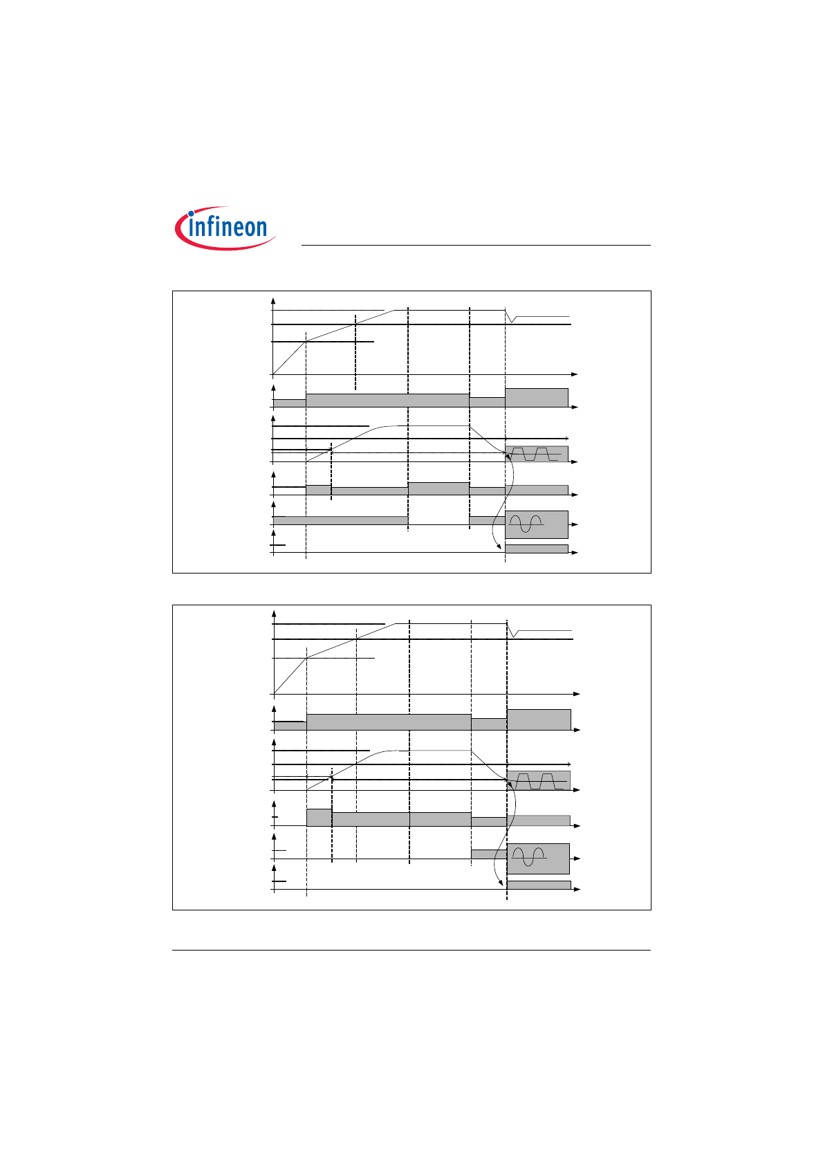
Figure 3
Start-up with LS filament broken and subsequent lamp removal.
Figure 4
Start-up with HS filament broken and subsequent lamp removal.
V
CC
14,0V
10,5V
I
VCC
80µA
5mA
+ QGate
V
RES
1,6V
I
RES
20µA
I
LVS
>15µA
3,2V
UVLO
START-UP
HYSTERESIS
IC ACTIVE
SOFTSTART
t
t
t
t
t
< +/- 2,5mA
17µA
34µA
17µA
20µA
16,0V
LS FILAMENT OPEN
HS FILAMENT CLOSED
LAMP REMOVAL
LS + HS OPEN
1,3V
POWER
DOWN
SIGNAL
t
20µA
5,0V
H
V
RES
> 1,3V
80µA
<170µA
>15µA
>15µA
<3,2V
<150µA
V
CC
14,0V
10,5V
I
VCC
80µA
5mA
+ QGate
V
RES
1,6V
I
RES
20µA
I
LVS
>15µA
3,2V
UVLO
IC ACTIVE
SOFTSTART
t
t
t
t
t
< +/- 2,5mA
34µA
34µA
17µA
20µA
16,0V
LAMP REMOVAL
LS + HS OPEN
V
RES
> 1,3V
1,3V
POWER
DOWN
SIGNAL
t
41µA
5,0V
H
<3,2V
<170µA
80µA
START-UP
HYSTERESIS
HS FILAMENT OPEN
LS FILAMENT CLOSED
>15µA
1,3V
<150µA