

MOSFET
MetalOxideSemiconductorFieldEffectTransistor
CoolMOS™C7
650VCoolMOS™C7PowerTransistor
IPB65R045C7
DataSheet
Rev.2.1
Final
PowerManagement&Multimarket
2
650VCoolMOS™C7PowerTransistor
IPB65R045C7
Rev.2.1,2013-04-30
Final Data Sheet
1
2
3
tab
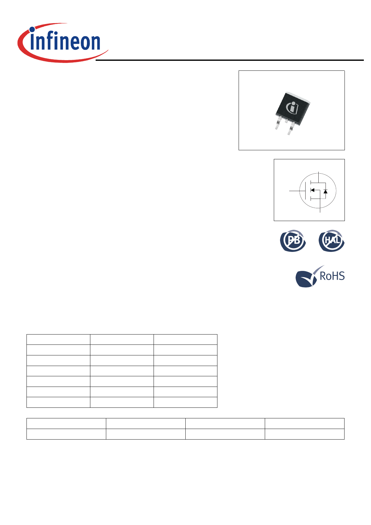
D²PAK
Drain
Pin 2, tab
Gate
Pin 1
Source
Pin 3
1Description
CoolMOS™isarevolutionarytechnologyforhighvoltagepower
MOSFETs,designedaccordingtothesuperjunction(SJ)principleand
pioneeredbyInfineonTechnologies.
CoolMOS™C7seriescombinestheexperienceoftheleadingSJ
MOSFETsupplierwithhighclassinnovation.Theproductportfolio
providesallbenefitsoffastswitchingsuperjunctionMOSFETsoffering
betterefficiency,reducedgatecharge,easyimplementationand
outstandingreliability.
Features
•IncreasedMOSFETdv/dtruggedness
•BetterefficiencyduetobestinclassFOMR
DS(on)
*E
oss
andR
DS(on)
*Q
g
•BestinclassR
DS(on)
/package
•Easytouse/drive
•Pb-freeplating,halogenfreemoldcompound
•QualifiedforindustrialgradeapplicationsaccordingtoJEDEC(J-STD20
andJESD22)
Benefits
•Enablinghighersystemefficiency
•Enablinghigherfrequency/increasedpowerdensitysolutions
•Systemcost/sizesavingsduetoreducedcoolingrequirements
•Highersystemreliabilityduetoloweroperatingtemperatures
Applications
PFCstagesandhardswitchingPWMstagesfore.g.Computing,Server,
Telecom,UPSandSolar.
Pleasenote:ForMOSFETparallelingtheuseofferritebeadsonthegate
orseparatetotempolesisgenerallyrecommended.
Table1KeyPerformanceParameters
Parameter
Value
Unit
V
DS
@ T
j,max
700
V
R
DS(on),max
45
m
Ω
Q
g.typ
93
nC
I
D,pulse
212
A
E
oss
@400V
11.7
µJ
Body diode di/dt
60
A/µs
Type/OrderingCode
Package
Marking
RelatedLinks
IPB65R045C7
PG-TO 263
65C7045
see Appendix A

3
650VCoolMOS™C7PowerTransistor
IPB65R045C7
Rev.2.1,2013-04-30
Final Data Sheet
TableofContents
Description . . . . . . . . . . . . . . . . . . . . . . . . . . . . . . . . . . . . . . . . . . . . . . . . . . . . . . . . . . . . . . . . . . . . . . . . . . . . . 2
Maximum ratings . . . . . . . . . . . . . . . . . . . . . . . . . . . . . . . . . . . . . . . . . . . . . . . . . . . . . . . . . . . . . . . . . . . . . . . . 4
Thermal characteristics . . . . . . . . . . . . . . . . . . . . . . . . . . . . . . . . . . . . . . . . . . . . . . . . . . . . . . . . . . . . . . . . . . . . 5
Electrical characteristics . . . . . . . . . . . . . . . . . . . . . . . . . . . . . . . . . . . . . . . . . . . . . . . . . . . . . . . . . . . . . . . . . . . 6
Electrical characteristics diagrams . . . . . . . . . . . . . . . . . . . . . . . . . . . . . . . . . . . . . . . . . . . . . . . . . . . . . . . . . . . 8
Test Circuits . . . . . . . . . . . . . . . . . . . . . . . . . . . . . . . . . . . . . . . . . . . . . . . . . . . . . . . . . . . . . . . . . . . . . . . . . . . 12
Package Outlines . . . . . . . . . . . . . . . . . . . . . . . . . . . . . . . . . . . . . . . . . . . . . . . . . . . . . . . . . . . . . . . . . . . . . . . 13
Appendix A . . . . . . . . . . . . . . . . . . . . . . . . . . . . . . . . . . . . . . . . . . . . . . . . . . . . . . . . . . . . . . . . . . . . . . . . . . . . 14
Revision History . . . . . . . . . . . . . . . . . . . . . . . . . . . . . . . . . . . . . . . . . . . . . . . . . . . . . . . . . . . . . . . . . . . . . . . . 15
Disclaimer . . . . . . . . . . . . . . . . . . . . . . . . . . . . . . . . . . . . . . . . . . . . . . . . . . . . . . . . . . . . . . . . . . . . . . . . . . . . 15
4
650VCoolMOS™C7PowerTransistor
IPB65R045C7
Rev.2.1,2013-04-30
Final Data Sheet
2Maximumratings
atT
j
=25°C,unlessotherwisespecified
Table2Maximumratings
Values
Min.
Typ.
Max.
Parameter
Symbol
Unit Note/TestCondition
Continuous drain current
1)
I
D
-
-
-
-
46
29
A
T
C
=25°C
T
C
=100°C
Pulsed drain current
2)
I
D,pulse
-
-
212
A
T
C
=25°C
Avalanche energy, single pulse
E
AS
-
-
249
mJ
I
D
=12A; V
DD
=50V
Avalanche energy, repetitive
E
AR
-
-
1.25
mJ
I
D
=12A; V
DD
=50V
Avalanche current, single pulse
I
AS
-
-
12.0
A
-
MOSFET dv/dt ruggedness
dv/dt
-
-
100
V/ns
V
DS
=0...400V
Gate source voltage (static)
V
GS
-20
-
20
V
static;
Gate source voltage (dynamic)
V
GS
-30
-
30
V
AC (f>1 Hz)
Power dissipation
P
tot
-
-
227
W
T
C
=25°C
Storage temperature
T
stg
-55
-
150
°C
-
Operating junction temperature
T
j
-55
-
150
°C
-
Mounting torque
-
-
-
-
Ncm
-
Continuous diode forward current
I
S
-
-
46
A
T
C
=25°C
Diode pulse current
2)
I
S,pulse
-
-
212
A
T
C
=25°C
Reverse diode dv/dt
3)
dv/dt
-
-
1.5
V/ns
V
DS
=0...400V,I
SD
<=I
S
,T
j
=25°C
Maximum diode commutation speed
di
f
/dt
-
-
60
A/
µ
s
V
DS
=0...400V,I
SD
<=I
S
,T
j
=25°C
Insulation withstand voltage
V
ISO
-
-
n.a.
V
V
rms
,T
C
=25°C,t=1min
1)
Limited by T
j max
.
2)
Pulse width t
p
limited by T
j,max
3)
IdenticallowsideandhighsideswitchwithidenticalR
G
5
650VCoolMOS™C7PowerTransistor
IPB65R045C7
Rev.2.1,2013-04-30
Final Data Sheet
3Thermalcharacteristics
Table3Thermalcharacteristics
Values
Min.
Typ.
Max.
Parameter
Symbol
Unit Note/TestCondition
Thermal resistance, junction - case
R
thJC
-
-
0.55
°C/W -
Thermal resistance, junction - ambient
R
thJA
-
-
62
°C/W device on PCB, minimal footprint
Thermal resistance, junction - ambient
for SMD version
R
thJA
-
35
45
°C/W
Device on 40mm*40mm*1.5mm
epoxy PCB FR4 with 6cm² (one
layer, 70µm thickness) copper
area for drain connection and
cooling. PCB is vertical without air
stream cooling.
Soldering temperature, wave- & reflow
soldering allowed
T
sold
-
-
260
°C
reflow MSL1
6
650VCoolMOS™C7PowerTransistor
IPB65R045C7
Rev.2.1,2013-04-30
Final Data Sheet
4Electricalcharacteristics
atT
j
=25°C,unlessotherwisespecified
Table4Staticcharacteristics
Values
Min.
Typ.
Max.
Parameter
Symbol
Unit Note/TestCondition
Drain-source breakdown voltage
V
(BR)DSS
650
-
-
V
V
GS
=0V,I
D
=1mA
Gate threshold voltage
V
(GS)th
3
3.5
4
V
V
DS
=V
GS
,I
D
=1.25mA
Zero gate voltage drain current
I
DSS
-
-
-
20
2
-
µ
A
V
DS
=650,V
GS
=0V,T
j
=25°C
V
DS
=650,V
GS
=0V,T
j
=150°C
Gate-source leakage current
I
GSS
-
-
100
nA
V
GS
=20V,V
DS
=0V
Drain-source on-state resistance
R
DS(on)
-
-
0.040
0.096
0.045
-
Ω
V
GS
=10V,I
D
=24.9A,T
j
=25°C
V
GS
=10V,I
D
=24.9A,T
j
=150°C
Gate resistance
R
G
-
0.85
-
Ω
f=1MHz,opendrain
Table5Dynamiccharacteristics
Values
Min.
Typ.
Max.
Parameter
Symbol
Unit Note/TestCondition
Input capacitance
C
iss
-
4340
-
pF
V
GS
=0V,V
DS
=400V,f=250kHz
Output capacitance
C
oss
-
70
-
pF
V
GS
=0V,V
DS
=400V,f=250kHz
Effective output capacitance, energy
related
1)
C
o(er)
-
146
-
pF
V
GS
=0V,V
DS
=0...400V
Effective output capacitance, time related
2)
C
o(tr)
-
1630
-
pF
I
D
=constant,V
GS
=0V,V
DS
=0...400V
Turn-on delay time
t
d(on)
-
20
-
ns
V
DD
=400V,V
GS
=13V,I
D
=24.9A,
R
G
=3.3
Ω
Rise time
t
r
-
14
-
ns
V
DD
=400V,V
GS
=13V,I
D
=24.9A,
R
G
=3.3
Ω
Turn-off delay time
t
d(off)
-
82
-
ns
V
DD
=400V,V
GS
=13V,I
D
=24.9A,
R
G
=3.3
Ω
Fall time
t
f
-
7
-
ns
V
DD
=400V,V
GS
=13V,I
D
=24.9A,
R
G
=3.3
Ω
Table6Gatechargecharacteristics
Values
Min.
Typ.
Max.
Parameter
Symbol
Unit Note/TestCondition
Gate to source charge
Q
gs
-
23
-
nC
V
DD
=400V,I
D
=24.9A,V
GS
=0to10V
Gate to drain charge
Q
gd
-
30
-
nC
V
DD
=400V,I
D
=24.9A,V
GS
=0to10V
Gate charge total
Q
g
-
93
-
nC
V
DD
=400V,I
D
=24.9A,V
GS
=0to10V
Gate plateau voltage
V
plateau
-
5.4
-
V
V
DD
=400V,I
D
=24.9A,V
GS
=0to10V
1)
C
o(er)
isafixedcapacitancethatgivesthesamestoredenergyasC
oss
whileV
DS
isrisingfrom0to400V
2)
C
o(tr)
isafixedcapacitancethatgivesthesamechargingtimeasC
oss
whileV
DS
isrisingfrom0to400V

7
650VCoolMOS™C7PowerTransistor
IPB65R045C7
Rev.2.1,2013-04-30
Final Data Sheet
Table7Reversediodecharacteristics
Values
Min.
Typ.
Max.
Parameter
Symbol
Unit Note/TestCondition
Diode forward voltage
V
SD
-
0.9
-
V
V
GS
=0V,I
F
=24.9A,T
j
=25°C
Reverse recovery time
t
rr
-
725
-
ns
V
R
=400V,I
F
=46A,di
F
/dt=60A/µs
Reverse recovery charge
Q
rr
-
13
-
µC
V
R
=400V,I
F
=46A,di
F
/dt=60A/µs
Peak reverse recovery current
I
rrm
-
36
-
A
V
R
=400V,I
F
=46A,di
F
/dt=60A/µs
8
650VCoolMOS™C7PowerTransistor
IPB65R045C7
Rev.2.1,2013-04-30
Final Data Sheet
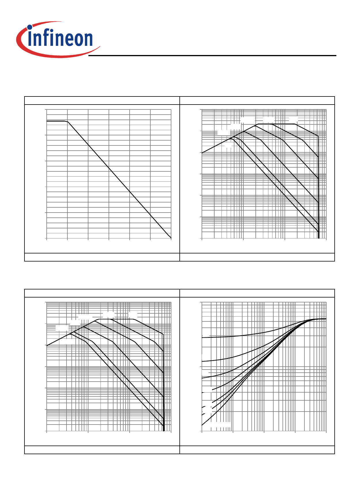
5Electricalcharacteristicsdiagrams
Table8
Diagram1:Powerdissipation
T
C
[°C]
P
tot
[W]
0
25
50
75
100
125
150
0
50
100
150
200
250
P
tot
=f(T
C
)
Diagram2:Safeoperatingarea
V
DS
[V]
I
D
[A]
10
0
10
1
10
2
10
3
10
-3
10
-2
10
-1
10
0
10
1
10
2
10
3
1 µs
10 µs
100 µs
1 ms
10 ms
DC
I
D
=f(V
DS
);T
C
=25°C;D=0;parameter:t
p
Table9
Diagram3:Safeoperatingarea
V
DS
[V]
I
D
[A]
10
0
10
1
10
2
10
3
10
-3
10
-2
10
-1
10
0
10
1
10
2
10
3
1 µs
10 µs
100 µs
1 ms
10 ms
DC
I
D
=f(V
DS
);T
C
=80°C;D=0;parameter:t
p
Diagram4:Max.transientthermalimpedance
t
p
[s]
Z
thJC
[K/W]
10
-5
10
-4
10
-3
10
-2
10
-1
10
-2
10
-1
10
0
0.5
0.2
0.1
0.05
0.02
0.01
single pulse
Z
thJC
=f(t
P
);parameter:D=t
p
/T
9
650VCoolMOS™C7PowerTransistor
IPB65R045C7
Rev.2.1,2013-04-30
Final Data Sheet
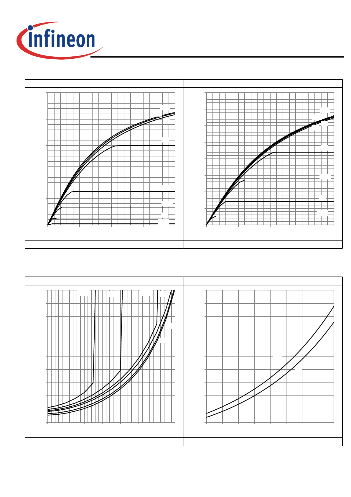
Table10
Diagram5:Typ.outputcharacteristics
V
DS
[V]
I
D
[A]
0
5
10
15
20
0
50
100
150
200
250
20 V
10 V
8 V
7 V
6 V
5.5 V
5 V
4.5 V
I
D
=f(V
DS
);T
j
=25°C;parameter:V
GS
Diagram6:Typ.outputcharacteristics
V
DS
[V]
I
D
[A]
0
5
10
15
20
0
20
40
60
80
100
120
140
160
20 V
10 V
8 V
7 V
6 V
5.5 V
5 V
4.5 V
I
D
=f(V
DS
);T
j
=125°C;parameter:V
GS
Table11
Diagram7:Typ.drain-sourceon-stateresistance
I
D
[A]
R
DS(on)
[
Ω
]
0
20
40
60
80
100
120
140
0.07
0.08
0.09
0.10
0.11
0.12
0.13
0.14
0.15
0.16
0.17
20 V
5.5 V
6 V
6.5 V
7 V
10 V
R
DS(on)
=f(I
D
);T
j
=125°C;parameter:V
GS
Diagram8:Drain-sourceon-stateresistance
T
j
[°C]
R
DS(on)
[
Ω
]
-50
-25
0
25
50
75
100
125
150
0.02
0.03
0.04
0.05
0.06
0.07
0.08
0.09
0.10
0.11
0.12
typ
98%
R
DS(on)
=f(T
j
);I
D
=24.9A;V
GS
=10V
10
650VCoolMOS™C7PowerTransistor
IPB65R045C7
Rev.2.1,2013-04-30
Final Data Sheet
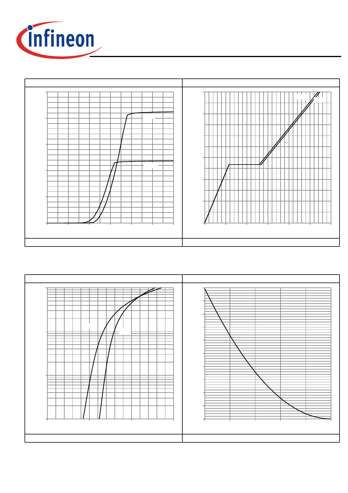
Table12
Diagram9:Typ.transfercharacteristics
V
GS
[V]
I
D
[A]
0
2
4
6
8
10
12
0
50
100
150
200
250
150 °C
25 °C
I
D
=f(V
GS
);V
DS
=20V;parameter:T
j
Diagram10:Typ.gatecharge
Q
gate
[nC]
V
GS
[V]
0
20
40
60
80
100
120
0
2
4
6
8
10
12
400 V
120 V
V
GS
=f(Q
gate
);I
D
=24.9Apulsed;parameter:V
DD
Table13
Diagram11:Forwardcharacteristicsofreversediode
V
SD
[V]
I
F
[A]
0.0
0.5
1.0
1.5
10
-1
10
0
10
1
10
2
125 °C
25 °C
I
F
=f(V
SD
);parameter:T
j
Diagram12:Avalancheenergy
T
j
[°C]
E
AS
[mJ]
25
50
75
100
125
150
0
25
50
75
100
125
150
175
200
225
250
E
AS
=f(T
j
);I
D
=12A;V
DD
=50V