
1
TechnicalInformation
6MS10017E41W36460
ModSTACK™
preparedby:OW
approvedby:AR
dateofpublication:2013-05-10
revision:2.0
Preliminarydata
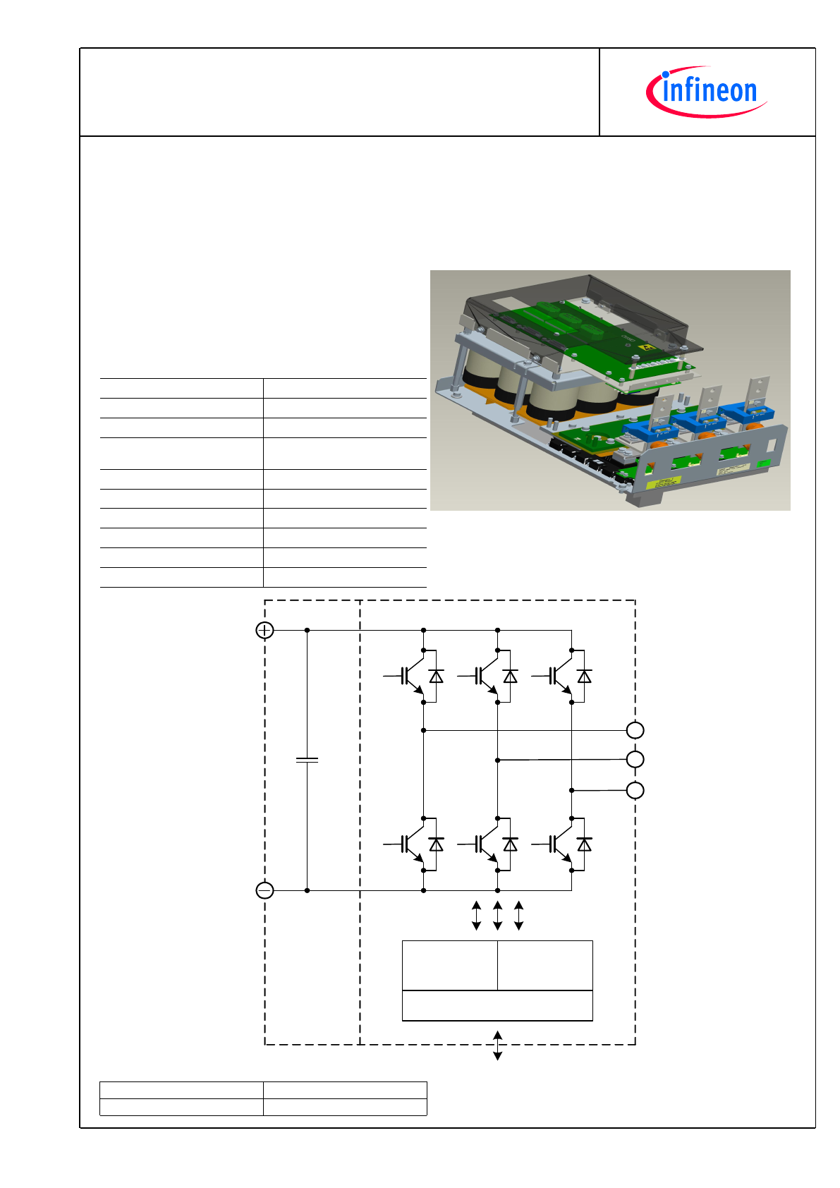
Generalinformation
IGBTStackfortypicalvoltagesofupto690V
RMS
Ratedoutputcurrent600A
RMS
· High power converter
· Wind power
· Motor drives
· PrimePACK
TM
3 module with integrated NTC
· Extended operational temperature
· Low V
cesat
Topology
B6I
Application
Inverter
Load type
Resistive, inductive
Semiconductor (Inverter
Section)
3x FF1000R17IE4
DC Link
3.6 mF
Heatsink
Water cooled
Implemented sensors
Current, voltage, temperature
Driver signals IGBT
Electrical
Sales - name
6MS10017E41W36460
SP - No.
SP000939300
DC Link
Inverter Section
Signal
conditioning
& monitor
Driver
3 phases
Electrical interface
~
~
~
2
TechnicalInformation
6MS10017E41W36460
ModSTACK™
preparedby:OW
approvedby:AR
dateofpublication:2013-05-10
revision:2.0
Preliminarydata
Absolutemaximumratedvalues
Collector-emitter voltage
IGBT; T
vj
= 25°C
V
CES
1700
V
Repetitive peak reverse voltage Diode; T
vj
= 25°C
V
RRM
1700
V
DC link voltage
V
DC
1250
V
Insulation management
according to installation height of 2000 m
V
line
690
V
RMS
Insulation test voltage
according to EN 50178, f = 50 Hz, t = 1 s
V
ISOL
2.5
kV
RMS
Repetitive peak collector
current inverter section (IGBT)
t
p
= 1 ms
I
CRM2
1250
A
Repetitive peak forward current
inverter section (Diode)
t
p
= 1 ms
I
FRM2
1250
A
I²t-value inverter section
(Diode)
I²t
140
kA²s
Continuous current inverter
section
I
AC2
710
A
RMS
Junction temperature
under switching conditions
T
vjop
150
°C
Switching frequency inverter
section
f
sw2
5
kHz
Notes
Further maximum ratings are specified in the following dedicated sections
Characteristicvalues
DCLink
min.
typ.
max.
Rated voltage
V
DC
1100
1250
V
Over voltage shutdown
within 150 µs
1250
V
Capacitor
1 s, 9 p, rated tol. +/- 10 %
C
DC
3.6
mF
type
Foil
Maximum ripple current
per device, T
amb
= 55 °C
I
ripple
49
A
RMS
Balance or discharge resistor
per DC link unit
R
b
47
k
Ω
Notes
Operation above 1100 V subject to reduced operating time according to EN 61071
InverterSection
min.
typ.
max.
Rated continuous current
V
DC
= 1100 V, V
AC
= 690 V
RMS
, cos(
ϕ
) = 0.85,
f
AC sine
= 50 Hz, f
sw
= 3000 Hz, T
inlet
= 40°C, T
j
≤
150 °C
I
AC
600
A
RMS
Continuous current at low
frequency
V
DC
= 1100 V, V
AC
= 690 V
RMS
, f
AC sine
= 0 Hz,
f
sw
= 3000 Hz, T
inlet
= 40 °C, T
j
≤
150 °C
I
AC low
295
A
RMS
Rated continuous current for
150% overload capability
I
AC 150%
= 610 A
RMS
, t
on over
= 60 s, T
j
≤
150 °C
I
AC over1
405
A
RMS
Rated continuous current for
150% overload capability
I
AC 150%
= 670 A
RMS
, t
on over
= 3 s, T
j
≤
150 °C
I
AC over2
445
A
RMS
Over current shutdown
within 15 µs
I
AC OC
1250
A
peak
Power losses
I
AC
= 600 A, V
DC
= 1100 V, V
AC
= 690 V
RMS
,
cos(
ϕ
) = 0.85, f
AC sine
= 50 Hz, f
sw
= 3000 Hz,
T
inlet
= 40 °C, T
j
≤
150 °C
P
loss
9800
W
3
TechnicalInformation
6MS10017E41W36460
ModSTACK™
preparedby:OW
approvedby:AR
dateofpublication:2013-05-10
revision:2.0
Preliminarydata
Controllerinterface
Driver and interface board
ref. to separate Application Note
DR110
min.
typ.
max.
Auxiliary voltage
V
aux
18
24
30
V
Auxiliary power requirement
V
aux
= 24 V
P
aux
40
W
Digital input level
resistor to GND 1.8 k
Ω
, capacitor to GND 4 nF,
logic high = on, min. 15 mA
V
in low
0
4
V
V
in high
11
15
V
Digital output level
open collector, logic low = no fault, max. 15 mA
V
out low
0
1.5
V
V
out high
15
V
Analog current sensor output
inverter section
load max 1 mA, @ 600 A
RMS
V
IU ana2
V
IV ana2
V
IW ana2
3.4
3.5
3.6
V
Analog DC link voltage sensor
output
load max 1 mA, @ 1100 V
V
DC ana
7.7
7.9
8..1
V
Analog temperature sensor
output inverter section (NTC)
load max 1 mA, @T
NTC
= 72 °C,
corresponds to T
j
= 148 °C at rated conditions
V
Theta NTC2
8.4
V
Analog temperature sensor
output inverter section
(Simulated)
load max 1 mA, @T
NTC
= 72 °C,
corresponds to T
j
= 148 °C at rated conditions
V
Theta sim2
9
V
Over temperature shutdown
inverter section
V
Error OT2
9.3
V
Systemdata
min.
typ.
max.
EMC robustness
according to IEC 61800-3 at named
interfaces
V
Burst
2
kV
power
V
Burst
1
kV
control
V
surge
1
kV
aux (24V)
Storage temperature
T
stor
-40
80
°C
Operational ambient
temperature
PCB, DC link capacitor, bus bar, excluding cooling
medium
T
op amb
-25
55
°C
Cooling air velocity
PCB, DC link capacitor, bus bar, standard atmosphere
V
air
2
m/s
Humidity
no condensation
Rel. F
0
95
%
Vibration
according to IEC 60721
5
m/s²
Shock
according to IEC 60721
40
m/s²
Protection degree
IP00
Pollution degree
2
Dimensions
width x depth x height
590
338
366
mm
Weight
65
kg
Heatsinkwatercooled
min.
typ.
max.
Water flow
according to coolant specification from Infineon
∆
V/
∆
t
15
dm³/min
Water pressure
8
bar
Water pressure drop
at 15 dm³/min water flow
∆
p
200
mbar
Coolant inlet temperature
T
inlet
-40
55
°C
Thermal resistance heatsink to
ambient
per switch
R
th,ha
0.038
K/W
Cooling channel material
Copper
Notes
Composition of coolant: Water and 52 vol. % Antifrogen N
4
TechnicalInformation
6MS10017E41W36460
ModSTACK™
preparedby:OW
approvedby:AR
dateofpublication:2013-05-10
revision:2.0
Preliminarydata
Overviewofoptionalcomponents
Unit 1
Inverter
Section
Unit 3
Parallel interface board
Optical interface board
Voltage sensor
×
Current sensor
×
Temperature sensor
×
Temperature simulation
×
DC link capacitors
×
Collector-emitter Active Clamping
×
Notes
Setting of Active Clamping TVS-Diodes: V
Z
= 1280 V
5
TechnicalInformation
6MS10017E41W36460
ModSTACK™
preparedby:OW
approvedby:AR
dateofpublication:2013-05-10
revision:2.0
Preliminarydata
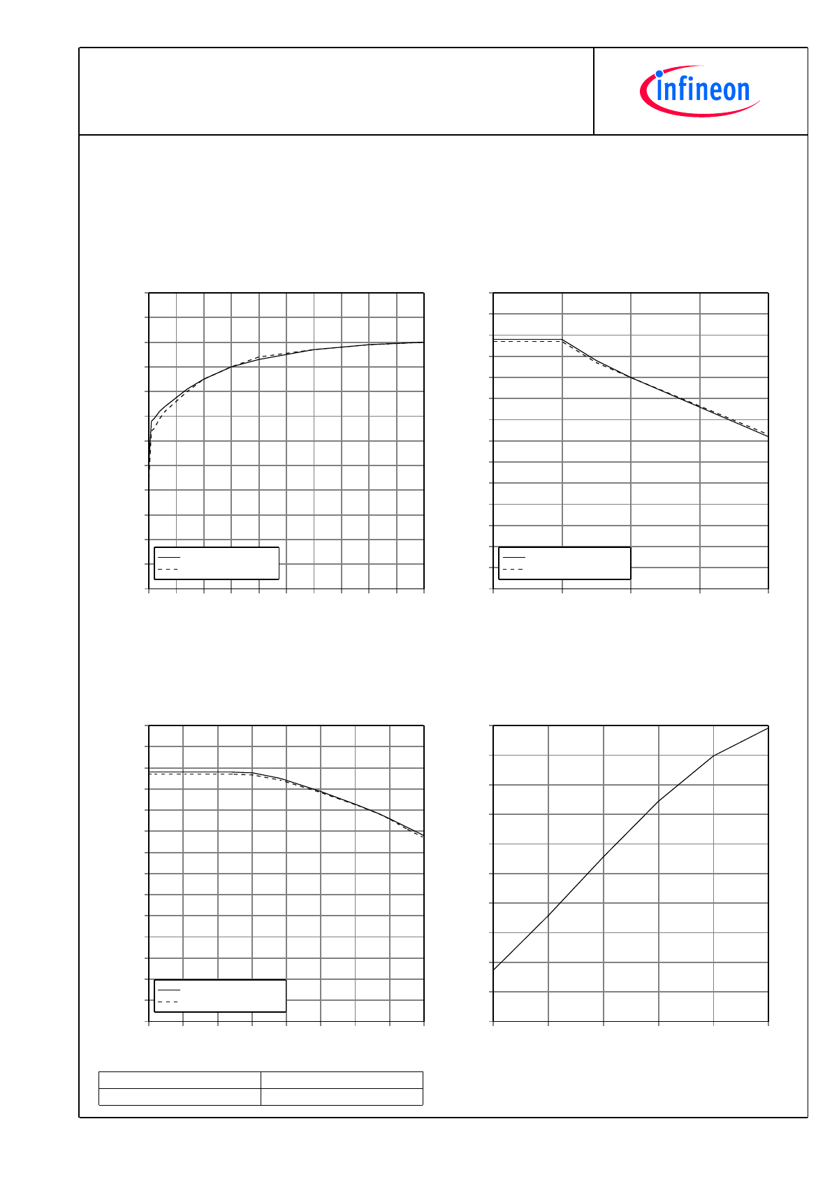
f
AC sine
- derating curve IGBT (motor), Diode (generator)
V
DC
= 1100 V, V
AC
= 690 V
RMS
, f
sw
= 3 kHz, cos
ϕ
= ±0.85
T
inlet
= 40°C and nom. cooling conditions
f
AC sine
[Hz]
I
AC
/I
nom
[%]
0
5
10
15
20
25
30
35
40
45
50
0
10
20
30
40
50
60
70
80
90
100
110
120
IGBT, cos
ϕ
= 0.85
IGBT, cos
ϕ
= 0.85
f
sw
- derating curve IGBT (motor), Diode (generator)
V
DC
= 1100 V, V
AC
= 690 V
RMS
, f
AC sine
= 50 Hz, cos
ϕ
= ±0.85
T
inlet
= 40°C and nom. cooling conditions
f
sw
[Hz]
I
AC
/I
nom
[%]
1000
2000
3000
4000
5000
0
10
20
30
40
50
60
70
80
90
100
110
120
130
140
IGBT, cos
ϕ
= 0.85
Diode, cos
ϕ
= -0.85
T
inlet
- derating curve IGBT (motor), Diode (generator)
V
DC
= 1100 V, V
AC
= 690 V
RMS
, f
AC sine
= 3 kHz, f
AC sine
= 50 Hz
cos
ϕ
= ±0.85 and nom. cooling conditions
T
inlet
[°C]
I
AC
/I
nom
[%]
-25
-15
-5
5
15
25
35
45
55
0
10
20
30
40
50
60
70
80
90
100
110
120
130
140
IGBT, cos
ϕ
= 0.85
Diode, cos
ϕ
= -0.85
Analog temperature sensor output V
Theta NTC
Sensing NTC of IGBT module
T
NTC
[°C]
V
Theta NTC
[V]
0
20
40
60
80
100
0
1
2
3
4
5
6
7
8
9
10
6
TechnicalInformation
6MS10017E41W36460
ModSTACK™
preparedby:OW
approvedby:AR
dateofpublication:2013-05-10
revision:2.0
Preliminarydata
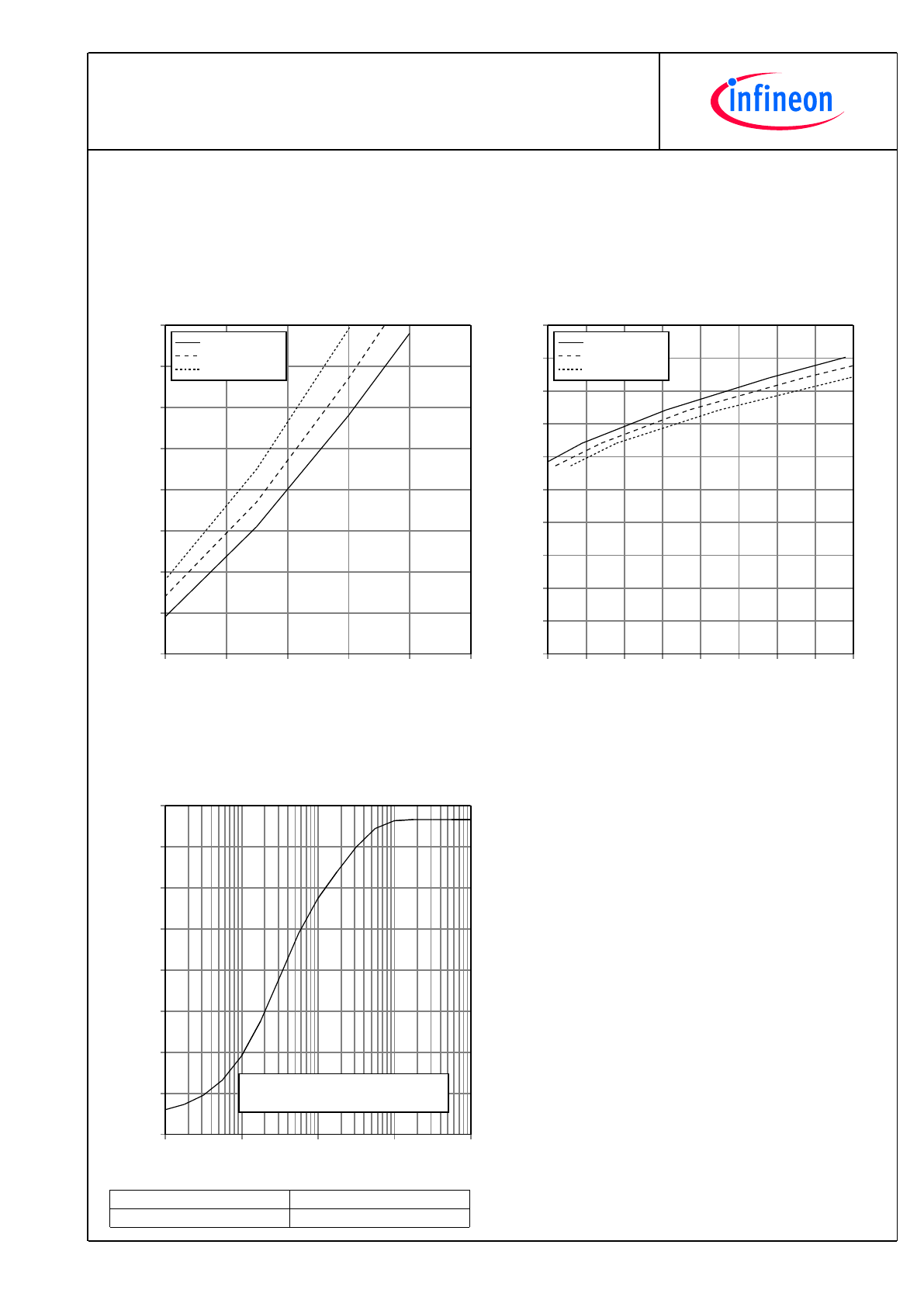
T
vj,sim
vs. I
AC
- Simulated junction temperature
V
DC
= 1100 V, V
AC
= 690 V
RMS
, f
sw
= 3 kHz
T
inlet
= 40°C and nom. cooling conditions
I
AC
[A]
T
vj,sim
[°C]
200
300
400
500
600
700
70
80
90
100
110
120
130
140
150
f
AC sine
= 50 Hz
f
AC sine
= 12 Hz
f
AC sine
= 5 Hz
Analog temperature sensor output V
Theta sim
V
DC
= 1100 V, V
AC
= 690 V
RMS
, f
sw
= 3 kHz,
T
inlet
= 40°C and nom. cooling conditions
T
vj,sim
[°C]
V
Theta sim
[V]
70
80
90
100
110
120
130
140
150
0
1
2
3
4
5
6
7
8
9
10
f
AC sine
= 50 Hz
f
AC sine
= 12 Hz
f
AC sine
= 5 Hz
Z
th,ha
- thermal impedance heatsink to ambient per switch
nom. cooling conditions
t [s]
Z
th,ha
[K/W]
0.1
1
10
100
1000
0.000
0.005
0.010
0.015
0.020
0.025
0.030
0.035
0.040
i:
r
i
[K/W]:
τ
i
[s]:
1
0.00214
0.0000005
2
0.0002
1.5299
3
0.02168
2.729
4
0.0143
21.884
7
TechnicalInformation
6MS10017E41W36460
ModSTACK™
preparedby:OW
approvedby:AR
dateofpublication:2013-05-10
revision:2.0
Preliminarydata
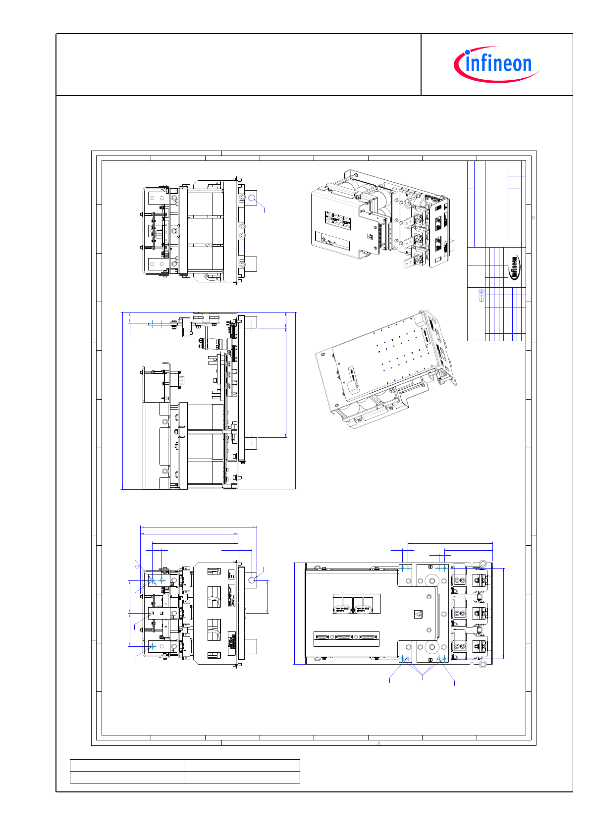
Mechanicaldrawing
1
H
2
3
4
5
6
7
8
9
10
11
12
1
2
3
4
5
6
8
7
G
F
E
D
C
B
A
H
G
F
E
D
C
B
A
9
10
11
12
C
op
yr
ig
ht
IN
F
IN
E
O
N
T
E
C
H
N
O
LO
G
IE
S
A
G
,A
ll
rig
ht
s
re
se
rv
ed
c
A
2
Do
ku
me
nts
ta
tu
ss
ie
he
SA
P-D
oku
me
nte
nve
rw
altu
ng
11
0
11
0
30
11
26
9.5
43
.5
11
0
36
.2
58
9
52
36
4.
5
33
8
59
0
30
2
15
1
26
6
18
18
36
5.1
30
6.6
P
ar
t-
N
o.
36
77
5
ge
ne
ra
lT
ol
er
an
ce
S
ur
fa
ce
S
ca
le
3:
10
A
ss
em
bl
y-
N
o.
D
IN
IS
O
27
68
-v
-
M
at
er
ia
l
M
at
er
ia
l-N
o.
D
at
e
N
am
e
D
es
ci
pt
io
n
A
ge
nt
12
.0
9.
20
11
P
el
m
er
M
od
S
TA
C
K
H
D
C
he
ck
ed
12
.0
9.
20
11
ge
z.
V
ol
ke
N
or
m
G
ra
ph
-N
o.
V
er
si
on
S
he
et
36
77
5
M
b
0
1/
1
01
A
bd
ec
ku
ng
ge
än
d.
16
.0
3.
12
P
a.
V
er
s.
R
ev
is
io
n
D
at
e
N
am
e
O
rig
in
C
on
st
ru
ct
ed
fo
r
D
C
P
lu
s
D
C
M
in
us
G
1/
2"
w
at
er
in
le
t
U
V
W
M
8x
27
.5
1:
5
1:
5
G
1/
2"
w
at
er
ou
tle
t
8
TechnicalInformation
6MS10017E41W36460
ModSTACK™
preparedby:OW
approvedby:AR
dateofpublication:2013-05-10
revision:2.0
Preliminarydata
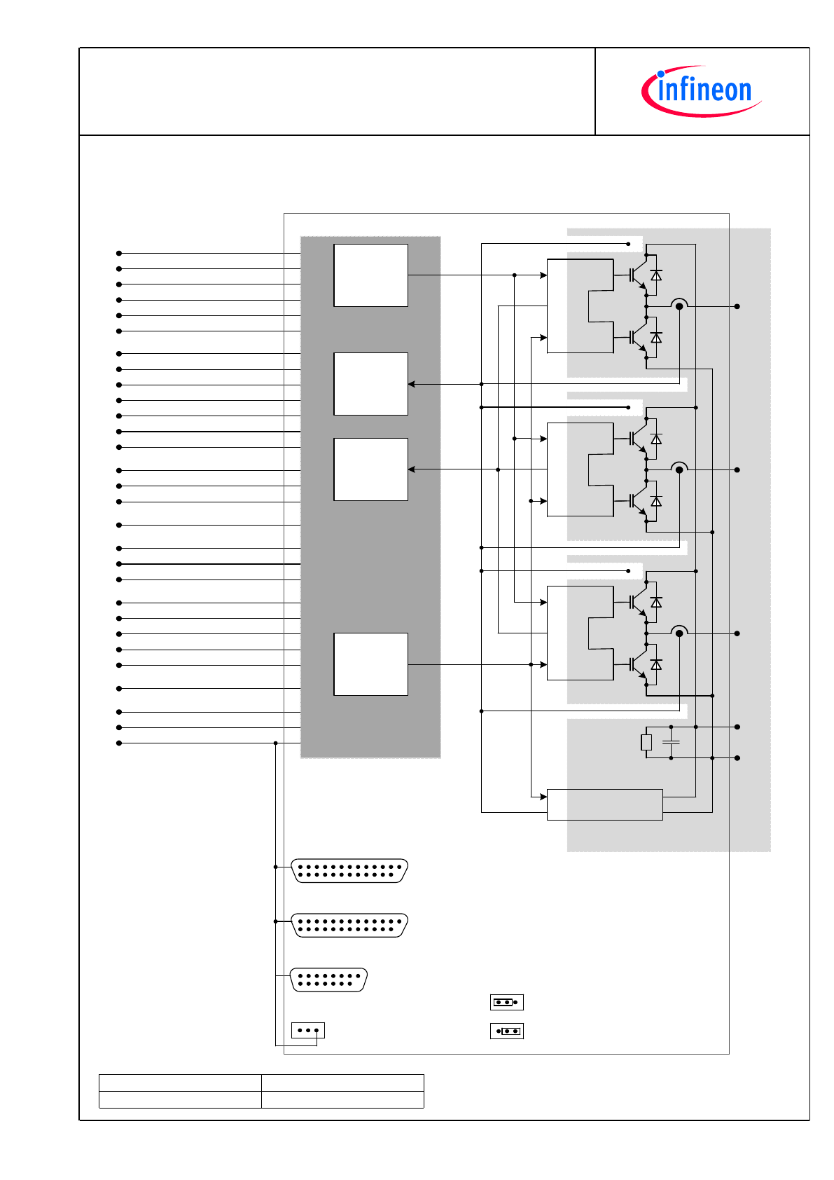
Circuitdiagram
Top
Bottom
E
ic
eD
R
IV
E
R
T
M
Top
Bottom
E
ic
eD
R
IV
E
R
T
M
Top
Bottom
E
ic
eD
R
IV
E
R
T
M
U
V
W
DC-
DC+
V-Option
Voltage measurement
T
NTC
T
NTC
T
NTC
Signal
conditioning
&
Gate signals
Sensor
signals
Failure
management
Power
supply
DR110
High voltage domain
Low voltage domain
M
od
S
T
A
C
K
T
M
H
D
1
13
14
25
X2 (male connector)
1
13
14
25
X3 (male connector)
1
8
9
15
X4 (male connector)
X2:14
PWM U BOT
X2:15
PWM U TOP
X2:3
PWM V BOT
X2:4
PWM V TOP
X2:17
PWM W BOT
X2:18
PWM W TOP
X2:2, X3:5
Phase U Error
X2:16, X3:18 Phase V Error
X2:5, X3:6
Phase W Error
X3:19
OT Error
X3:7
OV Error
X3:17
OC Error
X3:4
Sum Error
X2:10, X2:22 GND
digital
X3:2, X3:14
GND
digital
X4:9, X4:14
GND
digital
X2:8, X2:20
P24
X3:3, X3:15
15V
X4:15
15V
X4:13
-15V
X3:11
V
IU ana
X3:12
V
IV ana
X3:13
V
IW ana
X3:10
V
Theta NTC,
V
Theta sim
X3:23
V
DC ana
X3:24, X3:25 GND
analog
X5:1
V
aux
X5:2
GND
X5:3
TE, Shield
X5 (male connector)
1
3
Th
Tj
SV1 (jumper)
Setting X3:10 = V
Theta NTC
Setting X3:10 = V
Theta sim
(Sensing NTC of IGBT module)
(Simulated junction temperature)
(default setting)

9
TechnicalInformation
6MS10017E41W36460
ModSTACK™
preparedby:OW
approvedby:AR
dateofpublication:2013-05-10
revision:2.0
Preliminarydata
Terms&Conditionsofusage
Thedatacontainedinthisproductdatasheetisexclusivelyintendedfortechnicallytrainedstaff.Youandyourtechnical
departmentswillhavetoevaluatethesuitabilityoftheproductfortheintendedapplicationandthecompletenessoftheproduct
datawithrespecttosuchapplication.
Thisproductdatasheetisdescribingthecharacteristicsofthisproductforwhichawarrantyisgranted.Anysuchwarrantyis
grantedexclusivelypursuantthetermsandconditionsofthesupplyagreement.Therewillbenoguaranteeofanykindforthe
productanditscharacteristics.
Shouldyourequireproductinformationinexcessofthedatagiveninthisproductdatasheetorwhichconcernsthespecific
applicationofourproduct,pleasecontactthesalesoffice,whichisresponsibleforyou(seewww.infineon.com,sales&contact).
Forthosethatarespecificallyinterestedwemayprovideapplicationnotes.
Duetotechnicalrequirementsourproductmaycontaindangeroussubstances.Forinformationonthetypesinquestionplease
contactthesalesoffice,whichisresponsibleforyou.
ShouldyouintendtousetheProductinaviationapplications,inhealthorliveendangeringorlifesupportapplications,please
notify.Pleasenote,thatforanysuchapplicationsweurgentlyrecommend
-toperformjointRiskandQualityAssessments;
-theconclusionofQualityAgreements;
-toestablishjointmeasuresofanongoingproductsurvey,
andthatwemaymakedeliverydependedontherealization
ofanysuchmeasures.
Ifandtotheextentnecessary,pleaseforwardequivalentnoticestoyourcustomers.
Changesofthisproductdatasheetarereserved.
SafetyInstructions
Priortoinstallationandoperation,allsafetynoticesandwarningsandallwarningsignsattachedtotheequipmenthavetobe
carefullyread.Makesurethatallwarningsignsremaininalegibleconditionandthatmissingordamagedsignsarereplaced.To
installationandoperation,allsafetynoticesandwarningsandallwarningsignsattachedtotheequipmenthavetobecarefully
read.Makesurethatallwarningsignsremaininalegibleconditionandthatmissingordamagedsignsarereplaced.