

BTS5210G
Smart High-Side Power Switch
PROFET
Data Sheet, Rev. 1.3, April 2009
Automotive
Data Sheet
2
Rev. 1.3, 2009-04-16
Smart High-Side Power Switch
BTS5210G
6PDUW+LJK6LGH3RZHU6ZLWFK
7ZR&KDQQHOV[PΩ
6WDWXV)HHGEDFN
Product Summary Package
2SHUDWLQJ9ROWDJH
9
EE
9
$FWLYHFKDQQHOV RQH
WZRSDUDOOHO
2QVWDWH5HVLVWDQFH
5
21
PΩ
PΩ
1RPLQDOORDGFXUUHQW
,
/120
$
$
&XUUHQWOLPLWDWLRQ
,
/6&U
$
$
*HQHUDO'HVFULSWLRQ
• 1FKDQQHOYHUWLFDOSRZHU026)(7ZLWKFKDUJHSXPSJURXQGUHIHUHQFHG&026FRPSDWLEOHLQSXWDQG
GLDJQRVWLFIHHGEDFNPRQROLWKLFDOO\LQWHJUDWHGLQ6PDUW6,3026
®
WHFKQRORJ\
• 3URYLGLQJHPEHGGHGSURWHFWLYHIXQFWLRQV
$SSOLFDWLRQV
• &FRPSDWLEOHKLJKVLGHSRZHUVZLWFKZLWKGLDJQRVWLFIHHGEDFNIRU9DQG9JURXQGHGORDGV
• $OOW\SHVRIUHVLVWLYHLQGXFWLYHDQGFDSDFLWYHORDGV
• 0RVWVXLWDEOHIRUORDGVZLWKKLJKLQUXVKFXUUHQWVVRDVODPSV
• 5HSODFHVHOHFWURPHFKDQLFDOUHOD\VIXVHVDQGGLVFUHWHFLUFXLWV
%DVLF)XQFWLRQV
• 9HU\ORZVWDQGE\FXUUHQW
• &026FRPSDWLEOHLQSXW
• ,PSURYHGHOHFWURPDJQHWLFFRPSDWLELOLW\(0&
• )DVWGHPDJQHWL]DWLRQRILQGXFWLYHORDGV
• 6WDEOHEHKDYLRXUDWXQGHUYROWDJH
• :LGHRSHUDWLQJYROWDJHUDQJH
• /RJLFJURXQGLQGHSHQGHQWIURPORDGJURXQG
3URWHFWLRQ)XQFWLRQV
Block Diagram
• 6KRUWFLUFXLWSURWHFWLRQ
• 2YHUORDGSURWHFWLRQ
• &XUUHQWOLPLWDWLRQ
• 7KHUPDOVKXWGRZQ
• 2YHUYROWDJHSURWHFWLRQLQFOXGLQJORDGGXPSZLWKH[WHUQDO
UHVLVWRU
• 5HYHUVHEDWWHU\SURWHFWLRQZLWKH[WHUQDOUHVLVWRU
• /RVVRIJURXQGDQGORVVRI9
EE
SURWHFWLRQ
• (OHFWURVWDWLFGLVFKDUJHSURWHFWLRQ(6'
'LDJQRVWLF)XQFWLRQ
• 'LDJQRVWLFIHHGEDFNZLWKRSHQGUDLQRXWSXW
• 2SHQORDGGHWHFWLRQLQ2))VWDWH
• )HHGEDFNRIWKHUPDOVKXWGRZQLQ21VWDWH
9EE
*1'
/RDG
/RDG
/RJLF
&KDQQHO
&KDQQHO
,1
67
,1
67
P-DSO-14
PG-DSO-14-37
•
AEC Qualified
•
Green product (RoHS compliant)
Data Sheet
3
Rev. 1.3, 2009-04-16
Smart High-Side Power Switch
BTS5210G
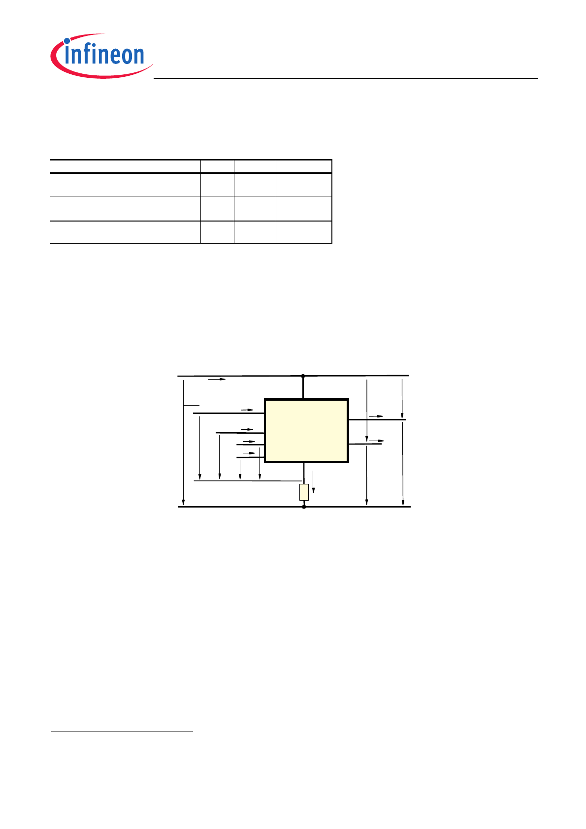
)XQFWLRQDOGLDJUDP
FKDQQHO
287
ORJLF
LQWHUQDO
YROWDJHVXSSO\
(6'
WHPSHUDWXUH
VHQVRU
FODPSIRU
LQGXFWLYHORDG
JDWH
FRQWURO
FKDUJH
SXPS
FXUUHQWOLPLW
UHYHUVH
EDWWHU\
SURWHFWLRQ
2SHQORDG
GHWHFWLRQ
control and protection circuit
equivalent to
channel 1
,1
9%%
*1'
,1
287
67
67
Data Sheet
4
Rev. 1.3, 2009-04-16
Smart High-Side Power Switch
BTS5210G
Pin Definitions and Functions
Pin
Symbol
Function
1,7,
8,14
V
bb
Positive power supply voltage. Design the
wiring for the simultaneous max. short circuit
currents from channel 1 to 2 and also for low
thermal resistance
2 GND
Logic Ground
3 IN1
5 IN2
Input 1,2 activates channel 1,2 in case
of logic high signal
4 ST1
6 ST2
Diagnostic feedback 1,2 of channel 1,2
open drain
12,13 OUT1
Output 1,2 protected high-side power output of
channel 1,2. Design the wiring for the max.
short circuit current; both output pins have to
9,10 OUT2
be connected in parallel for operation
according this spec.
11 NC Not Connected
Pin configuration
(top view)
V
bb
1
•
14 V
bb
GND 2
13 OUT1
IN1 3
12 OUT1
ST1 4
11 NC
IN2 5
10 OUT2
ST2 6
9 OUT2
V
bb
7
8 V
bb

Data Sheet
5
Rev. 1.3, 2009-04-16
Smart High-Side Power Switch
BTS5210G
Parameter Symbol
Values
Unit
Supply voltage (overvoltage protection see page 6)
V
bb
43
V
Supply voltage for full short circuit protection
T
j,start
= -40 ...+150°C
V
bb
36
V
Load current (Short-circuit current, see page 6)
I
L
self-limited
A
Load dump protection
1
)
V
LoadDump
=
V
A
+
V
s
,
V
A
= 13.5 V
R
I
2
)
= 2
Ω, t
d
= 400 ms; IN = low or high,
each channel loaded with
R
L
= 13.5
Ω,
V
Load dump
3
)
60
V
Operating temperature range
Storage temperature range
T
j
T
stg
-40 ...+150
-55 ...+150
°C
Power dissipation (DC)
4)
T
a
= 25°C:
(all channels active)
T
a
= 85°C:
P
tot
3,05
1,59
W
Maximal switchable inductance, single pulse
V
bb
= 12V,
T
j,start
= 150°C
4)
,
see diagrams on page 10
I
L
= 2.9 A,
E
AS
= 65 mJ, 0
Ω one
channel:
I
L
= 5.7 A,
E
AS
= 125 mJ, 0
Ω
two parallel channels:
Z
L
11,2
5,6
mH
Electrostatic discharge capability (ESD)
IN:
(Human Body Model)
ST:
out to all other pins shorted:
acc. MIL-STD883D, method 3015.7 and ESD assn. std. S5.1-1993
R=1.5k
Ω; C=100pF
V
ESD
1.0
4.0
8.0
kV
Input voltage (DC)
see internal circuit diagram page 9
V
IN
-10 ... +16
V
Current through input pin (DC)
Pulsed current through input pin
5
)
Current through status pin (DC)
I
IN
I
INp
I
ST
±0.3
±5.0
±5.0
mA
1
) Supply voltages higher than V
bb(AZ)
require an external current limit for the GND and status pins (a 150
Ω
resistor for the GND connection is recommended.
2)
R
I
= internal resistance of the load dump test pulse generator
3)
V
Load dump
is setup without the DUT connected to the generator per ISO 7637-1 and DIN 40839
4
) Device on 50mm*50mm*1.5mm epoxy PCB FR4 with 6cm
2
(one layer, 70
μm thick) copper area for Vbb
connection. PCB is vertical without blown air. See page 14
5
) only for testing
Data Sheet
6
Rev. 1.3, 2009-04-16
Smart High-Side Power Switch
BTS5210G
Parameter and Conditions
Symbol
Values
Unit
min typ
max
Thermal resistance
junction - soldering point
6)7)
each
channel:
R
thjs
-- --
15
K/W
junction – ambient
6)
@ 6 cm
2
cooling area
one channel active:
all channels active:
R
thja
--
--
--
--
45
40
--
--
--
Electrical Characteristics
Parameter and Conditions,
each of the four channels
Symbol
Values
Unit
at T
j
= -40...+150°C,
V
bb
= 12 V unless otherwise specified
min typ
max
Load Switching Capabilities and Characteristics
On-state resistance (Vbb to OUT);
IL = 2 A
each channel,
T
j
= 25°C:
T
j
= 150°C:
two parallel channels,
T
j
= 25°C:
see diagram, page 11
R
ON
--
--
--
110
210
55
140
280
70
m
Ω
Nominal load current
one channel active:
two parallel channels active:
Device on PCB
6)
,
T
a = 85°C,
T
j ≤ 150°C
I
L(NOM)
1.8
3.4
2.4
3.9
--
A
Output current
while GND disconnected or pulled up
8
)
;
Vbb = 32 V,
V
IN = 0,
see diagram page 9
I
L(GNDhigh)
-- -- 2
mA
Turn-on time
9
)
IN
to 90%
V
OUT
:
Turn-off time
IN
to 10%
V
OUT
:
R
L
= 12
Ω
t
on
t
off
--
--
100
100
250
270
μs
Slew rate on
9
)
10 to 30%
V
OUT
,
R
L
= 12
Ω: dV/dt
on
0.2 --
1.0
V/
μs
Slew rate off
9
)
70 to 40%
V
OUT
,
R
L
= 12
Ω: -dV/dt
off
0.2 --
1.1
V/
μs
6
) Device on 50mm*50mm*1.5mm epoxy PCB FR4 with 6cm
2
(one layer, 70
μm thick) copper area for Vbb
connection. PCB is vertical without blown air. See page 14
7
) Soldering point: upper side of solder edge of device pin 15. See page 14
8
) not subject to production test, specified by design
9
) See timing diagram on page 12.
Data Sheet
7
Rev. 1.3, 2009-04-16
Smart High-Side Power Switch
BTS5210G
Parameter and Conditions,
each of the four channels
Symbol
Values
Unit
at T
j
= -40...+150°C,
V
bb
= 12 V unless otherwise specified
min typ
max
Operating Parameters
Operating voltage
V
bb(on)
5.5
--
40
V
Undervoltage switch off
10
)
T
j
=-40°C...25°C
:
V
bb(u so)
--
--
4.5
V
T
j
=125°C:
--
-- 4.5
11)
Overvoltage protection
12
)
I
bb
= 40 mA
V
bb(AZ)
41
47
52
V
Standby current
13
)
T
j
=-40°C...25°C
:
V
IN
= 0;
see diagram page 11
T
j
=150°C:
I
bb(off)
--
--
5
--
8
12
μA
T
j
=125°C:
--
--
8
11)
Off-State output current (included in
I
bb(off)
)
V
IN
= 0; each channel
I
L(off)
-- 1 5
μA
Operating current
14)
,
V
IN
= 5V,
one channel on:
all channels on:
I
GND
--
--
0.5
1.0
0.9
1.7
mA
Protection Functions
15)
Current limit,
Vout = 0V
,
(see timing diagrams, page 12)
T
j
=-40°C:
T
j
=25°C:
T
j
=+150°C:
I
L(lim)
--
--
5
--
9
--
14
--
--
A
Repetitive short circuit current limit,
T
j
=
T
jt
each channel
two
channels
(see timing diagrams, page 12)
I
L(SCr)
--
--
6.5
6.5
--
--
A
Initial short circuit shutdown time
T
j,start
=25°C:
Vout = 0V
(see timing diagrams on page 12)
t
off(SC)
--
2
--
ms
Output clamp (inductive load switch off)
16)
at VON(CL) = Vbb - VOUT
,
IL= 40 mA
V
ON(CL)
41 47 52
V
Thermal overload trip temperature
T
jt
150 -- --
°C
Thermal hysteresis
ΔT
jt
-- 10 --
K
10)
is the voltage, where the device doesn´t change it´s switching condition for 15ms after the supply voltage
falling below the lower limit of Vbb(on)
11
) not subject to production test, specified by design
12
) Supply voltages higher than V
bb(AZ)
require an external current limit for the GND and status pins (a 150
Ω
resistor for the GND connection is recommended). See also
V
ON(CL)
in table of protection functions and
circuit diagram on page 9.
13
) Measured with load; for the whole device; all channels off
14
) Add I
ST
, if
I
ST
> 0
15
) Integrated protection functions are designed to prevent IC destruction under fault conditions described in the
data sheet. Fault conditions are considered as "outside" normal operating range. Protection functions are not
designed for continuous repetitive operation.
16
) If channels are connected in parallel, output clamp is usually accomplished by the channel with the lowest
V
ON(CL)
Data Sheet
8
Rev. 1.3, 2009-04-16
Smart High-Side Power Switch
BTS5210G
Parameter and Conditions,
each of the four channels
Symbol
Values
Unit
at T
j
= -40...+150°C,
V
bb
= 12 V unless otherwise specified
min typ
max
Reverse Battery
Reverse battery voltage
17
)
-
V
bb
--
--
32
V
Drain-source diode voltage
(V
out
> V
bb
)
I
L
= - 2.0 A,
T
j
= +150°C
-
V
ON
--
600
--
mV
Diagnostic Characteristics
Open load detection voltage
V
OUT(OL)
1
1.7 2.8 4.0
V
Input and Status Feedback
18
)
Input resistance
(see circuit page 9)
R
I
2.5
4.0 6.0
k
Ω
Input turn-on threshold voltage
V
IN(T+)
-- --
2.5
V
Input turn-off threshold voltage
V
IN(T-)
1.0 -- --
V
Input threshold hysteresis
Δ
V
IN(T)
-- 0.2 --
V
Status change after positive input slope
19)
with open load
t
d(STon)
-- 10 20
s
Status change after positive input slope
19)
with overload
t
d(STon)
30 -- --
s
Status change after negative input slope
with open load
t
d(SToff)
--
--
500
s
Status change after negative input slope
19)
with overtemperature
t
d(SToff)
--
--
20
s
Off state input current
V
IN
= 0.4 V:
I
IN(off)
5
-- 20
μA
On state input current
V
IN
= 5 V:
I
IN(on)
10 35 60
μA
Status output (open drain)
Zener limit voltage
I
ST
= +1.6 mA:
ST low voltage
I
ST
= +1.6 mA:
V
ST(high)
V
ST(low)
5.4
--
--
--
--
0.6
V
17
) Requires a 150 Ω resistor in GND connection. The reverse load current through the intrinsic drain-source
diode has to be limited by the connected load. Power dissipation is higher compared to normal operating
conditions due to the voltage drop across the drain-source diode. The temperature protection is not active
during reverse current operation! Input and Status currents have to be limited (see max. ratings page 4 and
circuit page 9).
18
) If ground resistors R
GND
are used, add the voltage drop across these resistors.
19
) not subject to production test, specified by design
Data Sheet
9
Rev. 1.3, 2009-04-16
Smart High-Side Power Switch
BTS5210G
Truth Table
( each channel )
IN
OUT
ST
Normal operation
L
H
L
H
H
H
Open load
L
H
Z
H
L
20
)
H
Overtemperature
L
H
L
L
H
L
L = "Low" Level
X = don't care
Z = high impedance, potential depends on external circuit
H = "High" Level
Status signal valid after the time delay shown in the timing diagrams
Parallel switching of channel 1 and 2 is easily possible by connecting the inputs and outputs in parallel (see truth
table). If switching channel 1 to 2 in parallel, the status outputs ST1 and ST2 have to be configured as a 'Wired
OR' function with a single pull-up resistor.
Terms
352)(7
,1
287
*1'
9EE
9
287
,
*1'
921
/HDGIUDPH
,1
9287
921
,/
287
9,1 9,1 , 67
,EE
,,1
, ,1
, 67
,/
5 *1'
9EE
967
967
67
67
Leadframe (V
bb
) is connected to pin 1,7,8,14
External R
GND
optional; single resistor R
GND
= 150
Ω for reverse battery protection up to the max.
operating voltage.
20
) L, if potential at the Output exceeds the OpenLoad detection voltage
Data Sheet
10
Rev. 1.3, 2009-04-16
Smart High-Side Power Switch
BTS5210G
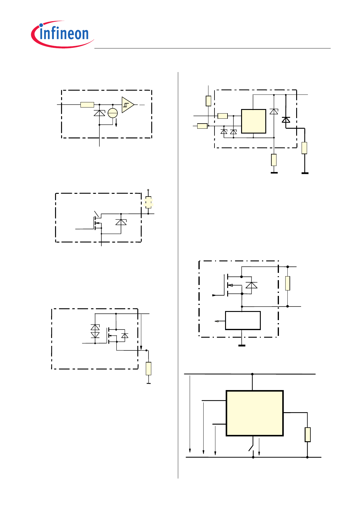
Input circuit (ESD protection),
IN1 or IN2
,1
*1'
,
5
(6'='
,,
,
The use of ESD zener diodes as voltage clamp at DC
conditions is not recommended.
Status output,
ST1 or ST2
67
*1'
(6'
='
9
5
6721
ESD-Zener diode: 6.1 V typ., max 0.3 mA; R
ST(ON)
< 375
Ω
at 1.6 mA. The use of ESD zener diodes as voltage clamp at
DC conditions is not recommended.
Inductive and overvoltage output clamp,
OUT1 or OUT2
9EE
287
9=
9
21
3RZHU*1'
V
ON
clamped to
V
ON(CL)
= 47 V typ.
Overvolt. and reverse batt. protection
9EE
,1
67
67
5
*1'
*1'
5
6LJQDO*1'
/RJLF
9=
,
5
9=
/RDG*1'
/RDG
5
287
67
5
9
V
Z1
= 6.1 V typ.,
V
Z2
= 47 V typ.,
R
GND
= 150
Ω,
R
ST
= 15 k
Ω, R
I
= 3.5 k
Ω typ.
In case of reverse battery the load current has to be
limited by the load. Temperature protection is not
active
Open-load detection,
OUT1 or OUT2
OFF-state diagnostic condition:
Open Load, if
V
OUT
> 3 V typ.; IN low
2SHQORDG
GHWHFWLRQ
/RJLF
XQLW
9287
6LJQDO*1'
2))
5(;7
9EE
GND disconnect
352)(7
9
,1
67
287
*1'
EE
9EE 9,1 967
9*1'
Any kind of load. In case of IN = high is
V
OUT
≈ V
IN
-
V
IN(T+)
.
Due to V
GND
> 0, no V
ST
= low signal available.