

MOSFET
MetalOxideSemiconductorFieldEffectTransistor
OptiMOS
TM
OptiMOS
TM
Power-MOSFET,25V
BSB012NE2LXI
DataSheet
Rev.2.1
Final
PowerManagement&Multimarket
2
OptiMOS
TM
Power-MOSFET,25V
BSB012NE2LXI
Rev.2.1,2015-09-09
Final Data Sheet
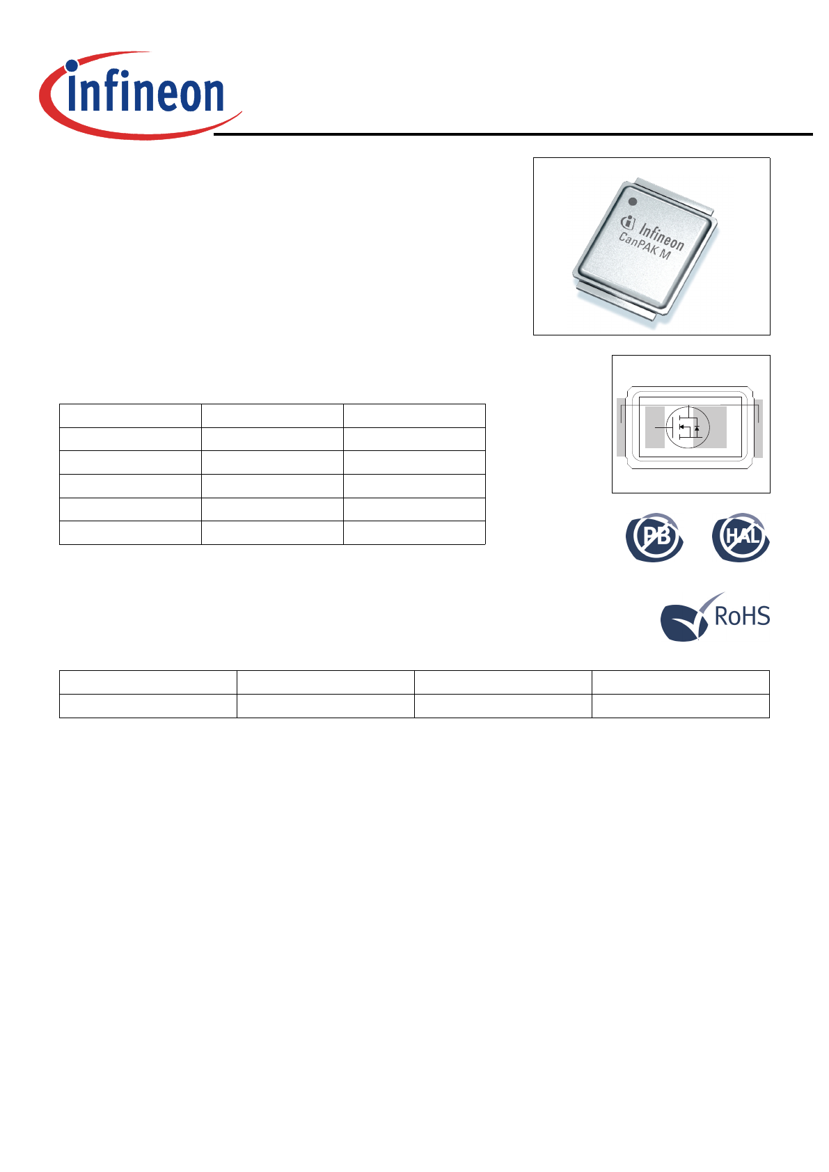
CanPAKM-size
Source
Gate
Drain
Drain
1Description
Features
•OptimizedSyncFETforhighperformanceBuckconverter
•IntegratedmonolithicSchottkylikediode
•Lowprofile(<0.7mm)
•100%avalanchetested
•100%R
G
Tested
•Double-sidedcooling
•CompatiblewithDirectFET®packageMXfootprintandoutline
1)
•QualifiedaccordingtoJEDEC
2)
fortargetapplications
•Pb-freeleadplating;RoHScompliant
Table1KeyPerformanceParameters
Parameter
Value
Unit
V
DS
25
V
R
DS(on),max
1.2
m
Ω
I
D
170
A
Q
oss
39
nC
Q
g
(0V..10V)
62
nC
Type/OrderingCode
Package
Marking
RelatedLinks
BSB012NE2LXI
MG-WDSON-2
05E2
-
1)
CanPAK
TM
uses DirectFET ® technology licensed from International Rectifier Corporation. DirectFET® is a registered
trademark of International Rectifier Corporation.
2)
J-STD20 and JESD22

3
OptiMOS
TM
Power-MOSFET,25V
BSB012NE2LXI
Rev.2.1,2015-09-09
Final Data Sheet
TableofContents
Description . . . . . . . . . . . . . . . . . . . . . . . . . . . . . . . . . . . . . . . . . . . . . . . . . . . . . . . . . . . . . . . . . . . . . . . . . . . . . 2
Maximum ratings . . . . . . . . . . . . . . . . . . . . . . . . . . . . . . . . . . . . . . . . . . . . . . . . . . . . . . . . . . . . . . . . . . . . . . . . 4
Thermal characteristics . . . . . . . . . . . . . . . . . . . . . . . . . . . . . . . . . . . . . . . . . . . . . . . . . . . . . . . . . . . . . . . . . . . . 4
Electrical characteristics . . . . . . . . . . . . . . . . . . . . . . . . . . . . . . . . . . . . . . . . . . . . . . . . . . . . . . . . . . . . . . . . . . . 5
Electrical characteristics diagrams . . . . . . . . . . . . . . . . . . . . . . . . . . . . . . . . . . . . . . . . . . . . . . . . . . . . . . . . . . . 7
Package Outlines . . . . . . . . . . . . . . . . . . . . . . . . . . . . . . . . . . . . . . . . . . . . . . . . . . . . . . . . . . . . . . . . . . . . . . . 11
Revision History . . . . . . . . . . . . . . . . . . . . . . . . . . . . . . . . . . . . . . . . . . . . . . . . . . . . . . . . . . . . . . . . . . . . . . . . 14
Disclaimer . . . . . . . . . . . . . . . . . . . . . . . . . . . . . . . . . . . . . . . . . . . . . . . . . . . . . . . . . . . . . . . . . . . . . . . . . . . . 14

4
OptiMOS
TM
Power-MOSFET,25V
BSB012NE2LXI
Rev.2.1,2015-09-09
Final Data Sheet
2Maximumratings
atT
j
=25°C,unlessotherwisespecified
Table2Maximumratings
Values
Min.
Typ.
Max.
Parameter
Symbol
Unit Note/TestCondition
Continuous drain current
I
D
-
-
-
-
-
-
170
107
37
A
V
GS
=10V,T
C
=25°C
V
GS
=10V,T
C
=100°C
V
GS
=10V,T
A
=25°C,R
thJA
=45K/W
1)
Pulsed drain current
2)
I
D,pulse
-
-
400
A
T
C
=25°C
Avalanche current, single pulse
3)
I
AS
-
-
40
A
T
C
=25°C
Avalanche energy, single pulse
E
AS
-
-
130
mJ
I
D
=40A,R
GS
=25
Ω
Gate source voltage
V
GS
-20
-
20
V
-
Power dissipation
P
tot
-
-
-
-
57
2.8
W
T
C
=25°C
T
A
=25°C,R
thJA
=45K/W
Operating and storage temperature
T
j
,T
stg
-40
-
150
°C
IEC climatic category;
DIN IEC 68-1: 40/150/56
3Thermalcharacteristics
Table3Thermalcharacteristics
Values
Min.
Typ.
Max.
Parameter
Symbol
Unit Note/TestCondition
Thermal resistance, junction - case,
bottom
R
thJC
-
1.0
-
K/W
-
Thermal resistance, junction - case,
top
R
thJC
-
-
2.2
K/W
-
Device on PCB,
6 cm
2
cooling area
1)
R
thJA
-
-
45
K/W
-
1)
Device on 40 mm x 40 mm x 1.5 mm epoxy PCB FR4 with 6 cm2 (one layer, 70 µm thick) copper area for drain
connection. PCB is vertical in still air.
2)
See figure 3 for more detailed information
3)
See figure 13 for more detailed information

5
OptiMOS
TM
Power-MOSFET,25V
BSB012NE2LXI
Rev.2.1,2015-09-09
Final Data Sheet
4Electricalcharacteristics
Table4Staticcharacteristics
Values
Min.
Typ.
Max.
Parameter
Symbol
Unit Note/TestCondition
Drain-source breakdown voltage
V
(BR)DSS
25
-
-
V
V
GS
=0V,I
D
=10mA
Breakdown voltage temperature
coefficient
dV
(BR)DSS
/dT
j
-
15
-
mV/K
I
D
=10mA,referencedto25°C
Gate threshold voltage
V
GS(th)
1.2
-
2
V
V
DS
=V
GS
,I
D
=250µA
Zero gate voltage drain current,
T
j
=25°C
I
DSS
-
25
500
µA
V
DS
=20V,V
GS
=0V
Zero gate voltage drain current,
T
j
=125°C
I
DSS
-
4
-
mA
V
DS
=20V,V
GS
=0V
Gate-source leakage current
I
GSS
-
10
100
nA
V
GS
=20V,V
DS
=0V
Drain-source on-state resistance
R
DS(on)
-
-
1.3
1.0
1.6
1.2
m
Ω
V
GS
=4.5V,I
D
=30A
V
GS
=10V,I
D
=30A
Gate resistance
R
G
0.3
0.6
1.2
Ω
-
Transconductance
g
fs
95
190
-
S
|V
DS
|>2|I
D
|R
DS(on)max
,I
D
=30A
Table5Dynamiccharacteristics
Values
Min.
Typ.
Max.
Parameter
Symbol
Unit Note/TestCondition
Input capacitance
C
iss
-
4400
5900
pF
V
GS
=0V,V
DS
=12V,f=1MHz
Output capacitance
C
oss
-
1900
2600
pF
V
GS
=0V,V
DS
=12V,f=1MHz
Reverse transfer capacitance
C
rss
-
190
-
pF
V
GS
=0V,V
DS
=12V,f=1MHz
Turn-on delay time
t
d(on)
-
5.4
-
ns
V
DD
=12V,V
GS
=10V,I
D
=30A,
R
G,ext
=1.6
Ω
Rise time
t
r
-
6.4
-
ns
V
DD
=12V,V
GS
=10V,I
D
=30A,
R
G,ext
=1.6
Ω
Turn-off delay time
t
d(off)
-
32
-
ns
V
DD
=12V,V
GS
=10V,I
D
=30A,
R
G,ext
=1.6
Ω
Fall time
t
f
-
4.8
-
ns
V
DD
=12V,V
GS
=10V,I
D
=30A,
R
G,ext
=1.6
Ω

6
OptiMOS
TM
Power-MOSFET,25V
BSB012NE2LXI
Rev.2.1,2015-09-09
Final Data Sheet
Table6Gatechargecharacteristics
1)
Values
Min.
Typ.
Max.
Parameter
Symbol
Unit Note/TestCondition
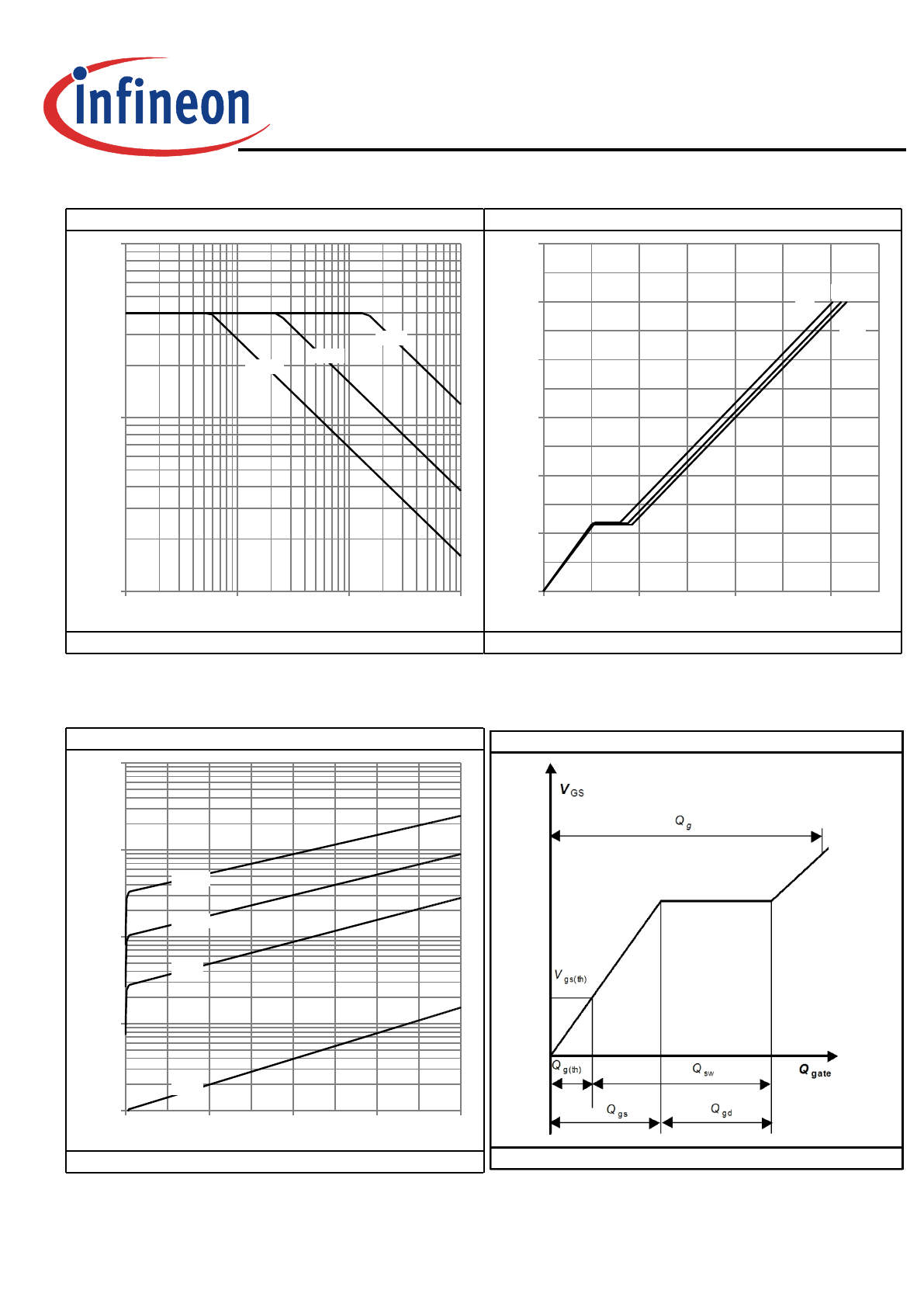
Gate to source charge
Q
gs
-
10.5
14
nC
V
DD
=12V,I
D
=30A,V
GS
=0to4.5V
Gate charge at threshold
Q
g(th)
-
7.1
-
nC
V
DD
=12V,I
D
=30A,V
GS
=0to4.5V
Gate to drain charge
Q
gd
-
7.3
11
nC
V
DD
=12V,I
D
=30A,V
GS
=0to4.5V
Switching charge
Q
sw
-
10.7
-
nC
V
DD
=12V,I
D
=30A,V
GS
=0to4.5V
Gate charge total
Q
g
-
30
40
nC
V
DD
=12V,I
D
=30A,V
GS
=0to4.5V
Gate plateau voltage
V
plateau
-
2.4
-
V
V
DD
=12V,I
D
=30A,V
GS
=0to4.5V
Gate charge total
Q
g
-
62
82
nC
V
DD
=12V,I
D
=30A,V
GS
=0to10V
Gate charge total, sync. FET
Q
g(sync)
-
26
-
nC
V
DS
=0.1V,V
GS
=0to4.5V
Output charge
Q
oss
-
39
52
nC
V
DD
=12V,V
GS
=0V
Table7Reversediode
Values
Min.
Typ.
Max.
Parameter
Symbol
Unit Note/TestCondition
Diode continuous forward current
I
S
-
-
57
A
T
C
=25°C
Diode pulse current
I
S,pulse
-
-
227
A
T
C
=25°C
Diode forward voltage
V
SD
-
0.56
-
V
V
GS
=0V,I
F
=12A,T
j
=25°C
Reverse recovery charge
Q
rr
-
5
-
nC
V
R
=15V,I
F
=I
S
,di
F
/dt=400A/µs
1)
See
″
Gate charge waveforms
″
for parameter definition
7
OptiMOS
TM
Power-MOSFET,25V
BSB012NE2LXI
Rev.2.1,2015-09-09
Final Data Sheet
5Electricalcharacteristicsdiagrams
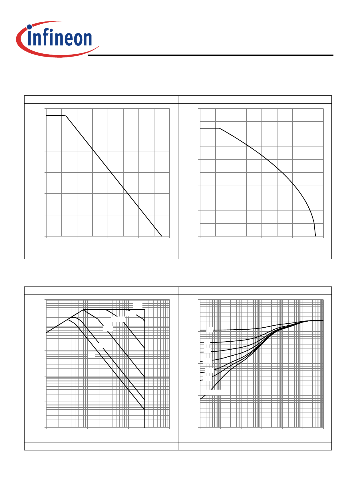
Diagram1:Powerdissipation
T
C
[°C]
P
tot
[W]
0
40
80
120
160
0
10
20
30
40
50
60
P
tot
=f(T
C
)
Diagram2:Draincurrent
T
C
[°C]
I
D
[A]
0
40
80
120
160
0
40
80
120
160
200
I
D
=f(T
C
);V
GS
≥
10V
Diagram3:Safeoperatingarea
V
DS
[V]
I
D
[A]
10
-1
10
0
10
1
10
2
10
-2
10
-1
10
0
10
1
10
2
10
3
1 µs
10 µs
100 µs
1 ms
10 ms
DC
I
D
=f(V
DS
);T
C
=25°C;D=0;parameter:t
p
Diagram4:Max.transientthermalimpedance
t
p
[s]
Z
thJC
[K/W]
10
-6
10
-5
10
-4
10
-3
10
-2
10
-1
10
0
10
-3
10
-2
10
-1
10
0
10
1
0.5
0.2
0.1
0.05
0.02
0.01
single pulse
Z
thJC
=f(t
p
);parameter:D=t
p
/T
8
OptiMOS
TM
Power-MOSFET,25V
BSB012NE2LXI
Rev.2.1,2015-09-09
Final Data Sheet
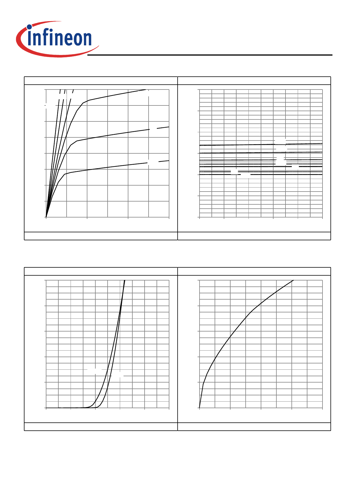
Diagram5:Typ.outputcharacteristics
V
DS
[V]
I
D
[A]
0
1
2
3
0
50
100
150
200
250
300
350
400
3.5 V
4.5 V
10 V
3.2 V
3 V
2.8 V
I
D
=f(V
DS
);T
j
=25°C;parameter:V
GS
Diagram6:Typ.drain-sourceonresistance
I
D
[A]
R
DS(on)
[m
Ω
]
0
10
20
30
40
50
0.0
0.5
1.0
1.5
2.0
2.5
3.0
3.2 V
3.5 V
4 V
4.5 V
5 V
7 V
10 V
R
DS(on)
=f(I
D
);T
j
=25°C;parameter:V
GS
Diagram7:Typ.transfercharacteristics
V
GS
[V]
I
D
[A]
0
1
2
3
4
5
0
80
160
240
320
400
150 °C
25 °C
I
D
=f(V
GS
);|V
DS
|>2|I
D
|R
DS(on)max
;parameter:T
j
Diagram8:Typ.forwardtransconductance
I
D
[A]
g
fs
[S]
0
40
80
120
160
0
80
160
240
320
400
g
fs
=f(I
D
);T
j
=25°C
9
OptiMOS
TM
Power-MOSFET,25V
BSB012NE2LXI
Rev.2.1,2015-09-09
Final Data Sheet
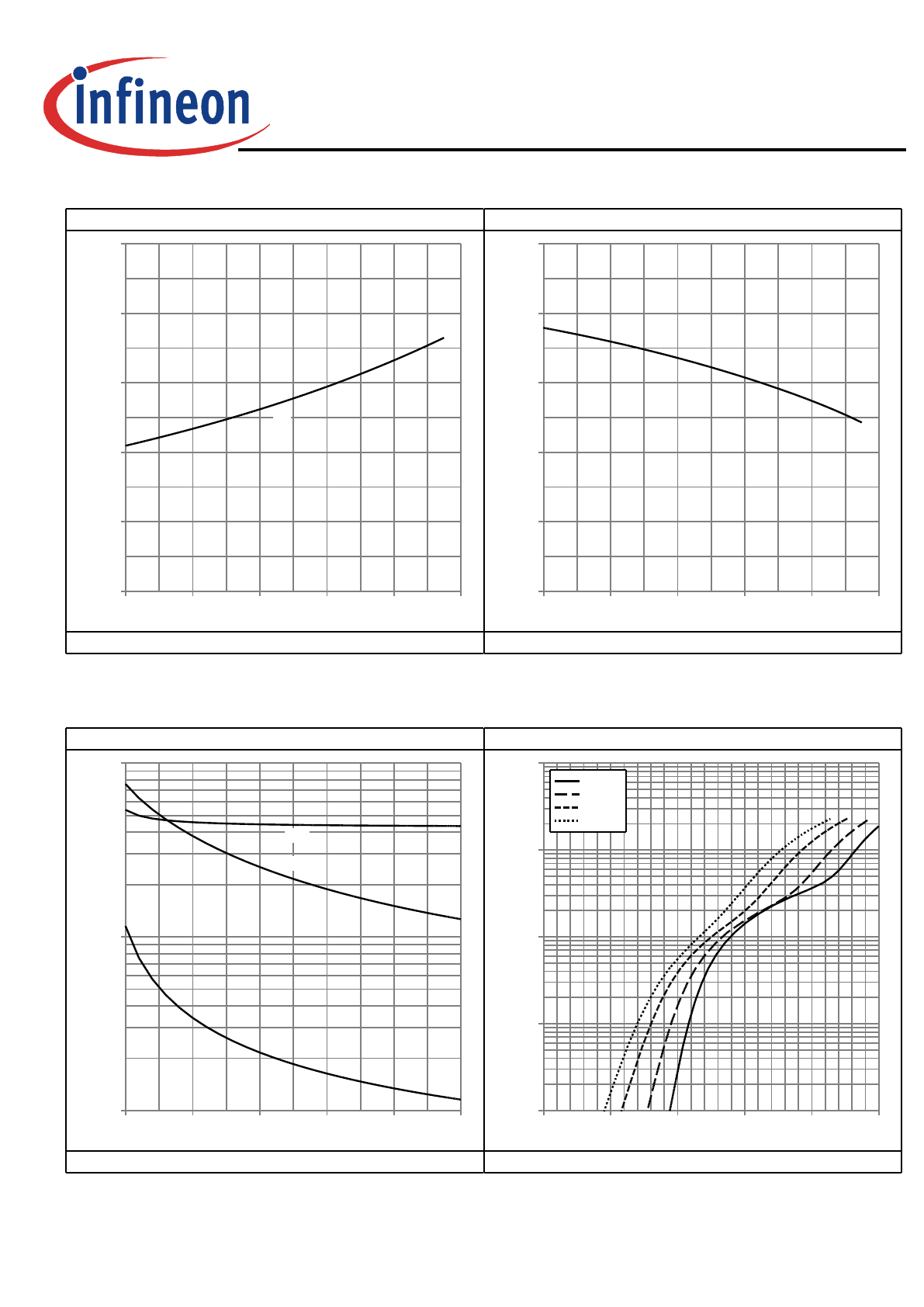
Diagram9:Drain-sourceon-stateresistance
T
j
[°C]
R
DS(on)
[m
Ω
]
-40
0
40
80
120
160
0.0
0.4
0.8
1.2
1.6
2.0
typ
R
DS(on)
=f(T
j
);I
D
=30A;V
GS
=10V
Diagram10:Typ.gatethresholdvoltage
T
j
[°C]
V
GS(th)
[V]
-40
0
40
80
120
160
0.0
0.5
1.0
1.5
2.0
2.5
V
GS(th)
=f(T
j
);V
GS
=V
DS
;I
D
=10mA
Diagram11:Typ.capacitances
V
DS
[V]
C
[pF]
0
5
10
15
20
25
10
2
10
3
10
4
Ciss
Coss
Crss
C=f(V
DS
);V
GS
=0V;f=1MHz
Diagram12:Forwardcharacteristicsofreversediode
V
SD
[V]
I
F
[A]
0.0
0.2
0.4
0.6
0.8
1.0
10
-1
10
0
10
1
10
2
10
3
-40 °C
25 °C
100 °C
150 °C
I
F
=f(V
SD
);parameter:T
j
10
OptiMOS
TM
Power-MOSFET,25V
BSB012NE2LXI
Rev.2.1,2015-09-09
Final Data Sheet
Diagram13:Avalanchecharacteristics
t
AV
[µs]
I
AV
[A]
10
0
10
1
10
2
10
3
10
0
10
1
10
2
25 °C
100 °C
125 °C
I
AS
=f(t
AV
);R
GS
=25
Ω
;parameter:T
j(start)
Diagram14:Typ.gatecharge
Q
gate
[nC]
V
GS
[V]
0
20
40
60
0
2
4
6
8
10
12
20 V
12 V
5 V
V
GS
=f(Q
gate
);I
D
=30Apulsed;parameter:V
DD
Diagram15:Typ.Drain-sourceleakagecurrent
V
DS
[V]
I
DSS
[A]
0
5
10
15
20
10
-6
10
-5
10
-4
10
-3
10
-2
125 °C
100 °C
75 °C
25 °C
I
DSS
=f(V
DS
);V
GS
=0V;parameter:T
j
Gate charge waveforms