
1
TechnicalInformation
6PS04512E43G37986
PrimeSTACK™
preparedby:OW
approvedby:AR
dateofpublication:2013-10-18
revision:2.2
Preliminarydata
Generalinformation
IGBTSTACKfortypicalvoltageofupto400V
Ratedoutputcurrent217A
- Solar power
- Motor drivers
- 62mm IGBT power module
· Trenchstop
TM
IGBT 4
Topology
B6I
Application
Inverter
Load type
Resistive, inductive
Semiconductor (Inverter
Section)
3 x FF450R12KE4
DC Link
2.4 mF
Heatsink
Forced air colled (fan not
included)
Implemented sensors
Current,voltage, temperature
Driver signals IGBT
Electrical
Design standards
EN 50178
Sales - name
6PS04512E43G37986
SP - No.
SP001046792
DC Link
Inverter Section
Signal
conditioning
& monitor
Driver
3 phases
Electrical interface
~
~
~
2
Technical Information
6PS04512E43G37986
PrimeSTACK™
prepared by: OW
approved by: AR
date of publication: 2013-10-18
revision: 2.2
Preliminary data
Absolute maximum rated values
Collector-emitter voltage
IGBT; T
vj
= 25°C
V
CES
1200
V
Repetitive peak reverse voltage Diode; T
vj
= 25°C
V
RRM
1200
V
DC link voltage
IGBT not swtiching
V
DC
900
V
Insulation management
according to installation height of 2000 m
V
line
500
V
RMS
Insulation test voltage
according to EN 50178, f = 50 Hz, t = 1 s
V
ISOL
2
kV
RMS
Repetitive peak collector
current inverter section (IGBT)
t
p
= 1 ms
I
CRM2
900
A
Repetitive peak forward current
inverter section (Diode)
t
p
= 1 ms
I
FRM2
900
A
Continuous current inverter
section
I
AC2
270
A
RMS
Junction temperature
under switching conditions
T
vjop
150
°C
Switching frequency inverter
section
f
sw2
14
kHz
Notes
Further maximun ratings are specified in the following dedicated sections
Characteristic values
DCLink
min.
typ.
max.
Rated voltage
V
DC
600
850
V
Over voltage shutdown
within 1000 µs
850
V
Capacitor
1 s, 6 p
C
DC
2.4
mF
Maximum ripple current
per device, T
amb
= 55 °C
I
ripple
49
A
RMS
Balance or discharge resistor
per DC link unit
R
b
164
k
Ω
InverterSection
min.
typ.
max.
Rated continuous current
V
DC
= 600 V, V
AC
= 400 V
RMS
, cos(
ϕ
) = 0.85,
f
AC sine
= 50 Hz, f
sw
= 5000 Hz, T
inlet
= 40°C, T
j
≤
125 °C
I
AC
265
A
RMS
Over current shutdown
within 15 µs
I
AC OC
626
A
peak
Power losses
I
AC
= 265 A, V
DC
= 600 V, V
AC
= 400 V
RMS
, cos(
ϕ
) = 0.85,
f
AC sine
= 50 Hz, f
sw
= 5000 Hz, T
inlet
= 40 °C, T
j
≤
125 °C
P
loss
2275
W
InverterSection(specificcondition)
min.
typ.
max.
Specific continuous current
V
DC
= 750 V, V
AC
= 400 V
RMS
, cos(
ϕ
) = 0.8,
f
AC sine
= 50 Hz, f
sw
= 5000 Hz, T
inlet
= 40 °C, T
j
≤
125 °C
I
ACsp
217
A
RMS
Continuous current at low
frequency
V
DC
= 750 V, V
AC
= 400 V
RMS
, cos(
ϕ
) = 0.8,
f
AC sine
= 0 Hz, f
sw
= 5000 Hz, T
inlet
= 40 °C, T
j
≤
125 °C
I
ACsp
105
A
RMS
Specific continuous current for
150% overload capability
I
AC 150%
= 263 A
RMS
, t
on over
= 3 s, T
j
≤
125 °C
I
ACsp over1
175
A
RMS
Specific continuous current for
150% overload capability
I
AC 150%
= 229 A
RMS
, t
on over
= 60 s, T
j
≤
125 °C
I
ACsp over2
152
A
RMS
Power losses
I
AC
= 217 A, V
DC
= 750 V, V
AC
= 400 V
RMS
, cos(
ϕ
) = 0.8,
f
AC sine
= 50 Hz, f
sw
= 5000 Hz, T
inlet
= 40 °C, T
j
≤
125 °C
P
loss
1975
W
Notes
Maximum junction temperature limited to 125°C under all operating conditions
3
Technical Information
6PS04512E43G37986
PrimeSTACK™
prepared by: OW
approved by: AR
date of publication: 2013-10-18
revision: 2.2
Preliminary data
Controllerinterface
Driver and interface board
ref. to separate Application Note
DR210
min.
typ.
max.
Auxiliary voltage
V
aux
18
24
30
V
Auxiliary power requirement
V
aux
= 24 V
P
aux
40
W
Digital input level
resistor to GND 10 k
Ω
, capacitor to GND 1 nF,
logic high = on
V
in low
0
1.5
V
V
in high
11
15
V
Digital output level
open collector, logic low = no fault, max. 15 mA
V
out low
0
1.5
V
V
out high
15
V
Analog current sensor output
inverter section
load max 5 mA, @ 217 A
RMS
V
IU ana2
V
IV ana2
V
IW ana2
3.3
3.5
3.7
V
Analog DC link voltage sensor
output
load max 5 mA, @ 850 V
V
DC ana
8.3
8.5
8.7
V
Analog temperature sensor
output unit 1 (NTC)
load max 5 mA, @T
NTC
= 85 °C,
corresponds to T
j
= 115 °C at rated conditions
V
Theta NTC1
10.7
10.9
11.1
V
Over temperature shutdown
inverter section
load max 5 mA, @T
NTC
= 87 °C
V
Error OT2
11
V
Systemdata
min.
typ.
max.
EMC robustness
according to EN 61800-3 at named
interfaces
V
Burst
2
kV
power
V
Burst
1
kV
control
V
surge
1
kV
aux (24V)
Storage temperature
T
stor
-40
80
°C
Operational ambient
temperature
PCB, DC link capacitor, bus bar, excluding cooling
medium
T
op amb
-25
55
°C
Cooling air velocity
PCB, DC link capacitor, bus bar, standard atmosphere
V
air
2
m/s
Humidity
no condensation
Rel. F
0
85
%
Vibration
according to IEC 60721
5
m/s²
Shock
according to IEC 60721
40
m/s²
Protection degree
IP00
Pollution degree
2
Dimensions
width x depth x height
216
335
376
mm
Weight
18
kg
Notes
Dimension "depth" does not include the data cables
Heatsinkaircooled
min.
typ.
max.
Air flow
T
air
= 25 °C, P
air
= 1013 hPa, dry and dust free,
measured at the side of the heat sink
according to DIN 41882
∆
V/
∆
t
500
m³/h
Air pressure drop
at min. air flow
∆
p
190
Pa
Air inlet temperature
T
inlet
-40
55
°C
4
Technical Information
6PS04512E43G37986
PrimeSTACK™
prepared by: OW
approved by: AR
date of publication: 2013-10-18
revision: 2.2
Preliminary data
Overview of optional components
Unit 1
Inverter
Section
Unit 3
Parallel interface board
Optical interface board
Chopper controller
Voltage sensor
×
Current sensor
×
Temperature sensor
×
Temperature simulation
DC link capacitors
×
Data cable for control signals
Fan
Collector-emitter Active Clamping
×
Notes
Setting of Active Clamping TVS-Diodes: V
Z
= 824 V
5
Technical Information
6PS04512E43G37986
PrimeSTACK™
prepared by: OW
approved by: AR
date of publication: 2013-10-18
revision: 2.2
Preliminary data
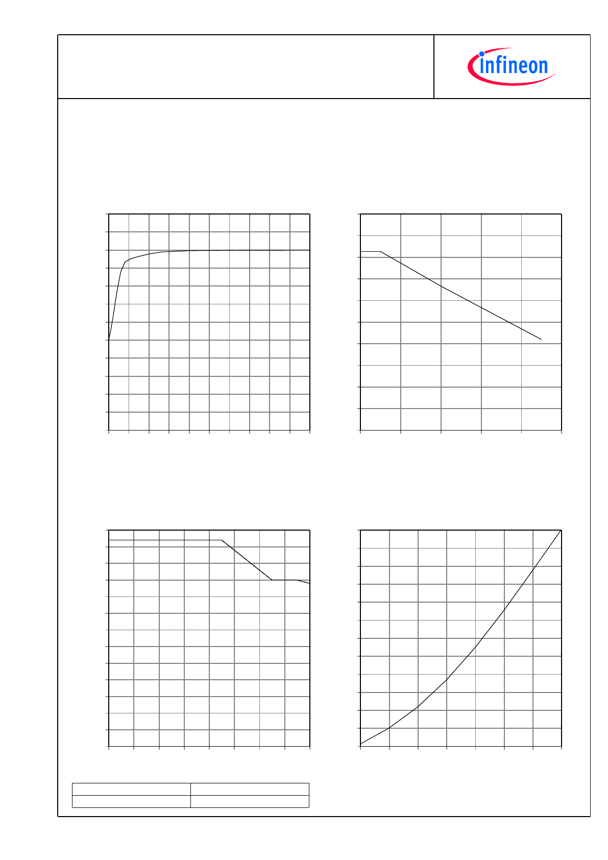
f
AC sine
- derating curve IGBT (motor), Diode (generator)
V
DC
= 750 V, V
AC
= 400 V
RMS
, f
sw
= 5 kHz, cos
ϕ
= ±0.8,
T
inlet
= 40 °C and nom. cooling conditions
f
AC sine
[Hz]
I
AC
/I
nom
[%]
0
5
10
15
20
25
30
35
40
45
50
0
10
20
30
40
50
60
70
80
90
100
110
120
f
sw
- derating curve IGBT (motor), Diode (generator)
V
DC
= 750 V, V
AC
= 400 V
RMS
, f
AC sine
= 50 Hz, cos
ϕ
= ±0.8,
T
inlet
= 40 °C and nom. cooling conditions
f
sw
[Hz]
I
AC
/I
nom
[%]
1000
3000
5000
7000
9000
11000
0
15
30
45
60
75
90
105
120
135
150
T
inlet
- derating curve IGBT (motor), Diode (generator)
V
DC
= 750 V, V
AC
= 400 V
RMS
, f
sw
= 5 kHz, f
AC sine
= 50 Hz,
cos
ϕ
= ±0.8 and nom. cooling conditions
T
inlet
[°C]
I
AC
/I
nom
[%]
-25
-15
-5
5
15
25
35
45
55
0
10
20
30
40
50
60
70
80
90
100
110
120
130
Analog temperature sensor output V
Theta NTC
Sensing NTC of heatsink
T
NTC
[°C]
V
Theta NTC
[V]
20
30
40
50
60
70
80
90
0
1
2
3
4
5
6
7
8
9
10
11
12
6
Technical Information
6PS04512E43G37986
PrimeSTACK™
prepared by: OW
approved by: AR
date of publication: 2013-10-18
revision: 2.2
Preliminary data
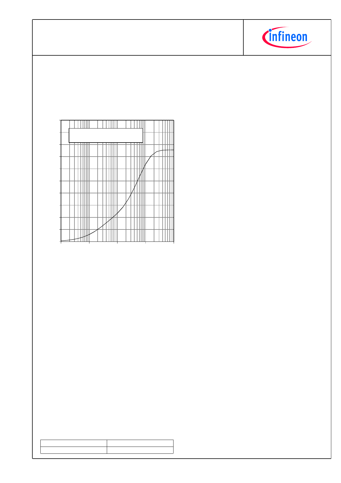
Z
th,ha
- thermal impedance heatsink to ambient per switch
nom. cooling conditions
t [s]
Z
th,ha
[K/W]
0.1
1
10
100
1000
0.00
0.02
0.04
0.06
0.08
0.10
0.12
0.14
0.16
0.18
0.20
i:
r
i
[K/W]:
τ
i
[s]:
1
0.02748
2.35
2
0.09086
51.34
3
0.03146
88.93
4
0.0012
88.93
7
Technical Information
6PS04512E43G37986
PrimeSTACK™
prepared by: OW
approved by: AR
date of publication: 2013-10-18
revision: 2.2
Preliminary data
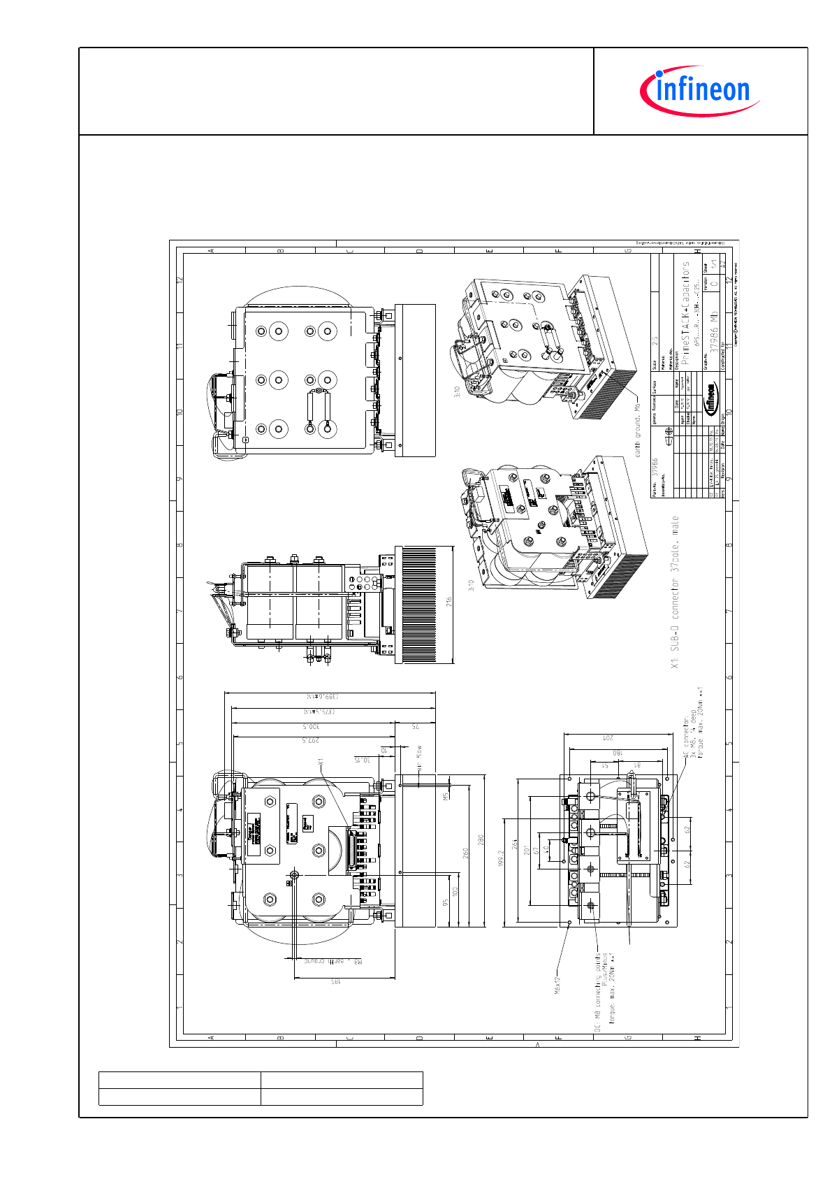
Mechanical drawing
8
Technical Information
6PS04512E43G37986
PrimeSTACK™
prepared by: OW
approved by: AR
date of publication: 2013-10-18
revision: 2.2
Preliminary data
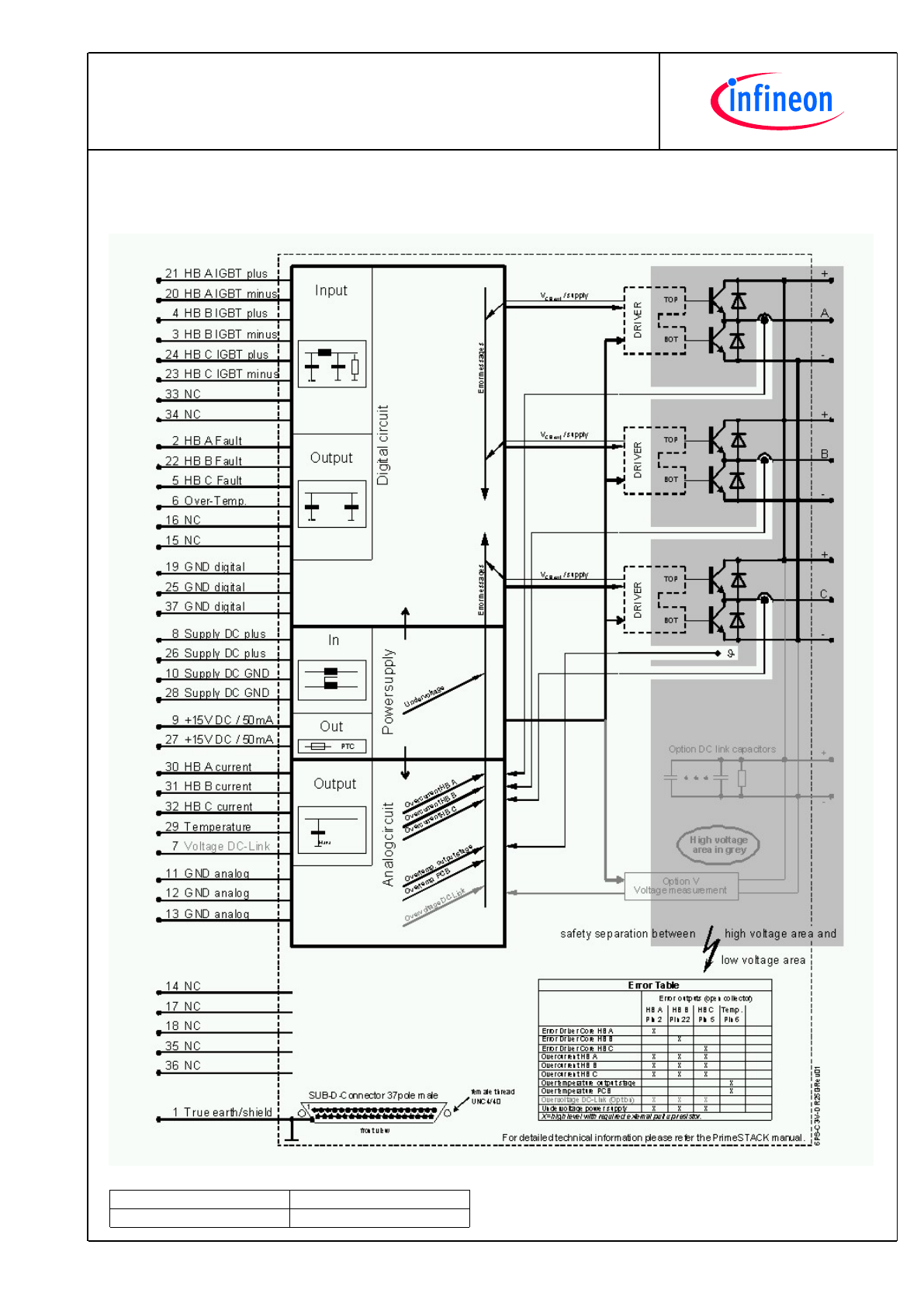
Circuit diagram
9
Technical Information
6PS04512E43G37986
PrimeSTACK™
prepared by: OW
approved by: AR
date of publication: 2013-10-18
revision: 2.2
Preliminary data
Terms & Conditions of usage
The data contained in this product data sheet is exclusively intended for technically trained staff. You and your technical departments will
have to evaluate the suitability of the product for the intended application and the completeness of the product data with respect to such
application.
This product data sheet is describing the characteristics of this product for which a warranty is granted. Any such warranty is granted
exclusively pursuant the terms and conditions of the supply agreement. There will be no guarantee of any kind for the product and its
characteristics.
Should you require product information in excess of the data given in this product data sheet or which concerns the specific application of
our product, please contact the sales office, which is responsible for you (see www.infineon.com, sales&contact). For those that are
specifically interested we may provide application notes.
Due to technical requirements our product may contain dangerous substances. For information on the types in question please contact the
sales office, which is responsible for you.
Should you intend to use the Product in aviation applications, in health or live endangering or life support applications, please notify.
Please note, that for any such applications we urgently recommend
- to perform joint Risk and Quality Assessments;
- the conclusion of Quality Agreements;
- to establish joint measures of an ongoing product survey,
and that we may make delivery depended on the realization
of any such measures.
If and to the extent necessary, please forward equivalent notices to your customers.
Changes of this product data sheet are reserved.
Safety Instructions
Prior to installation and operation, all safety notices and warnings and all warning signs attached to the equipment have to be carefully
read. Make sure that all warning signs remain in a legible condition and that missing or damaged signs are replaced. To installation and
operation, all safety notices and warnings and all warning signs attached to the equipment have to be carefully read. Make sure that all
warning signs remain in a legible condition and that missing or damaged signs are replaced.