
1
TechnicalInformation
2LS20017E42W36702
ModSTACK™
preparedby:OW
approvedby:AR
dateofpublication:2013-10-08
revision:2.2
Preliminarydata
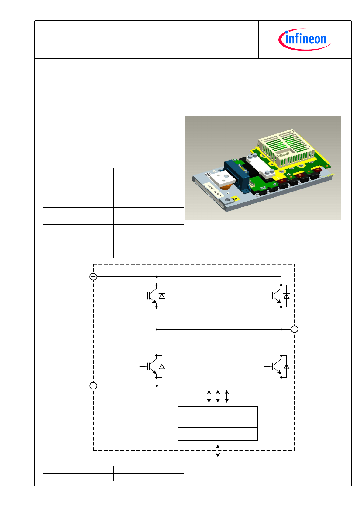
Generalinformation
IGBTStackfortypicalvoltagesofupto690V
RMS
Ratedoutputcurrent1520A
RMS
· High power converter
· Wind power
· Motor drives
· PrimePACK
TM
3 module
· Extended operational temperature
· Low V
cesat
Topology
1
/
2
B2I
Application
Inverter
Load type
Resistive, inductive
Semiconductor (Inverter
Section)
2x FF1000R17IE4
Heatsink
Water cooled
Implemented sensors
Current, temperature
Driver signals IGBT
Electrical
Design standards
EN 50178
Sales - name
2LS20017E42W36702
SP - No.
SP000934308
~
Inverter Section
Signal
conditioning
& monitor
Driver
1 phase
Electrical interface
2
TechnicalInformation
2LS20017E42W36702
ModSTACK™
preparedby:OW
approvedby:AR
dateofpublication:2013-10-08
revision:2.2
Preliminarydata
Absolutemaximumratedvalues
Collector-emitter voltage
IGBT; T
vj
= 25°C
V
CES
1700
V
Repetitive peak reverse voltage Diode; T
vj
= 25°C
V
RRM
1700
V
DC link voltage
V
DC
1250
V
Insulation management
according to installation height of 2000 m
V
line
690
V
RMS
Insulation test voltage
V
ISOL
2.5
kV
RMS
Repetitive peak collector
current inverter section (IGBT)
t
p
= 1 ms
I
CRM2
2500
A
Repetitive peak forward current
inverter section (Diode)
t
p
= 1 ms
I
FRM2
2500
A
Continuous current inverter
section
I
AC2
1660
A
RMS
Junction temperature
under switching conditions
T
vjop
150
°C
Switching frequency inverter
section
f
sw2
4
kHz
Notes
Further maximum ratings are specified in the following dedicated sections
Characteristicvalues
InverterSection
min.
typ.
max.
Rated continuous current
V
DC
= 1100 V, V
AC
= 690 V
RMS
, cos(
ϕ
) = 0.85,
f
AC sine
= 50 Hz, f
sw
= 2000 Hz, T
inlet
= 40°C, T
j
≤
150 °C
I
AC
1520
A
RMS
Continuous current at low
frequency
V
DC
= 1100 V, V
AC
= 690 V
RMS
, f
AC sine
= 0 Hz,
f
sw
= 2000 Hz, T
inlet
= 40 °C, T
j
≤
150 °C
I
AC low
770
A
RMS
Rated continuous current for
150% overload capability
I
AC 150%
= 1660 A
RMS
, t
on over
= 3 s, T
j
≤
150 °C
I
AC over1
1110
A
RMS
Over current shutdown
within 15 µs
I
AC OC
4200
A
peak
Power losses
I
AC
= 1520 A, V
DC
= 1100 V, V
AC
= 690 V
RMS
,
cos(
ϕ
) = 0.85, f
AC sine
= 50 Hz, f
sw
= 2000 Hz,
T
inlet
= 40 °C, T
j
≤
150 °C
P
loss
6700
W
Controllerinterface
Driver and interface board
ref. to separate Application Note
DR240
min.
typ.
max.
Auxiliary voltage
V
aux
18
24
30
V
Auxiliary power requirement
V
aux
= 24 V
P
aux
40
W
Digital input level
resistor to GND 1.8 k
Ω
, capacitor to GND 4 nF,
logic high = on, min. 15 mA
V
in low
0
4
V
V
in high
11
15
V
Digital output level
open collector, logic low = no fault, max. 15 mA
V
out low
0
1.5
V
V
out high
15
V
Analog current sensor output
inverter section
load max 1 mA, @ 1520 A
RMS
V
IU ana2
V
IV ana2
V
IW ana2
3.3
3.4
3.5
V
Analog temperature sensor
output inverter section (NTC)
load max 1 mA, @T
NTC
= 66 °C,
corresponds to T
j
= 150 °C at rated conditions
V
Theta NTC2
6.4
6.5
6.6
V
Over temperature shutdown
inverter section
load max 1 mA, @T
NTC
= 75 °C
V
Error OT2
8.6
V
3
TechnicalInformation
2LS20017E42W36702
ModSTACK™
preparedby:OW
approvedby:AR
dateofpublication:2013-10-08
revision:2.2
Preliminarydata
Systemdata
min.
typ.
max.
EMC robustness
according to IEC 61800-3 at named
interfaces
V
Burst
2
kV
power
V
Burst
1
kV
control
V
surge
1
kV
aux (24V)
Storage temperature
T
stor
-40
80
°C
Operational ambient
temperature
PCB, bus bar, excluding cooling medium
T
op amb
-25
55
°C
Humidity
no condensation
Rel. F
0
95
%
Vibration
5
m/s²
Shock
40
m/s²
Protection degree
IP00
Pollution degree
2
Dimensions
width x depth x height
205
400
117
mm
Weight
9
kg
Heatsinkwatercooled
min.
typ.
max.
Water flow
according to coolant specification from Infineon
∆
V/
∆
t
15
dm³/min
Water pressure
8
bar
Water pressure drop
∆
p
60
mbar
Coolant inlet temperature
T
inlet
-40
55
°C
Notes
Composition of coolant: Water and 52 vol. % Antifrogen N
Overviewofoptionalcomponents
Unit 1
Inverter
Section
Unit 3
Parallel interface board
Optical interface board
Voltage sensor
Current sensor
×
Temperature sensor
×
Temperature simulation
DC link capacitors
Data cable for control signals
Collector for water cooled heatsink
Collector-emitter Active Clamping
×
Notes
Setting of Active Clamping TVS-Diodes: V
Z
= 1280 V
4
TechnicalInformation
2LS20017E42W36702
ModSTACK™
preparedby:OW
approvedby:AR
dateofpublication:2013-10-08
revision:2.2
Preliminarydata
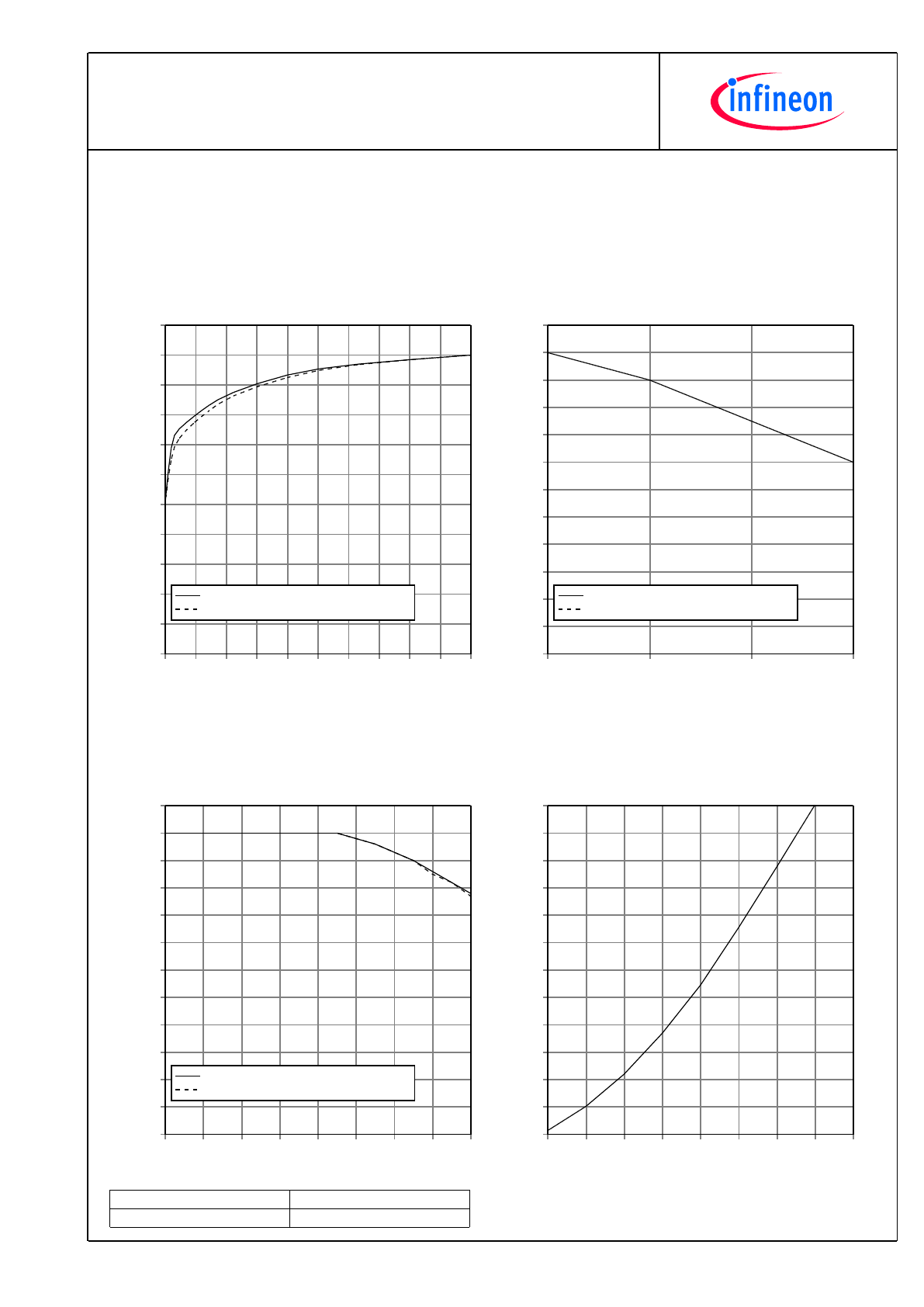
f
AC sine
- derating curve IGBT (motor), Diode (generator)
V
DC
= 1100 V, V
AC
= 690 V
RMS
, f
sw
= 2 kHz, cos
ϕ
= ±0.85,
T
inlet
= 40 °C and nom. cooling conditions
f
AC sine
[Hz]
I
AC
/I
nom
[%]
0
5
10
15
20
25
30
35
40
45
50
0
10
20
30
40
50
60
70
80
90
100
110
IGBT, cos
ϕ
= 0.85 (100% = 1520 A)
Diode, cos
ϕ
= -0.85 (100% = 1510 A)
f
sw
- derating curve IGBT (motor), Diode (generator)
V
DC
= 1100 V, V
AC
= 690 V
RMS
, f
AC sine
= 50 Hz, cos
ϕ
= ±0.85,
T
inlet
= 40 °C and nom. cooling conditions
f
sw
[Hz]
I
AC
/I
nom
[%]
1000
2000
3000
4000
0
10
20
30
40
50
60
70
80
90
100
110
120
IGBT, cos
ϕ
= 0.85 (100% = 1520 A)
Diode, cos
ϕ
= -0.85 (100% = 1510 A)
T
inlet
- derating curve IGBT (motor), Diode (generator)
V
DC
= 1100 V, V
AC
= 690 V
RMS
, f
sw
= 2 kHz, f
AC sine
= 50 Hz,
cos
ϕ
= ±0.85 and nom. cooling conditions
T
inlet
[°C]
I
AC
/I
nom
[%]
-25
-15
-5
5
15
25
35
45
55
0
10
20
30
40
50
60
70
80
90
100
110
120
IGBT, cos
ϕ
= 0.85 (100% = 1520 A)
Diode, cos
ϕ
= -0.85 (100% = 1510 A)
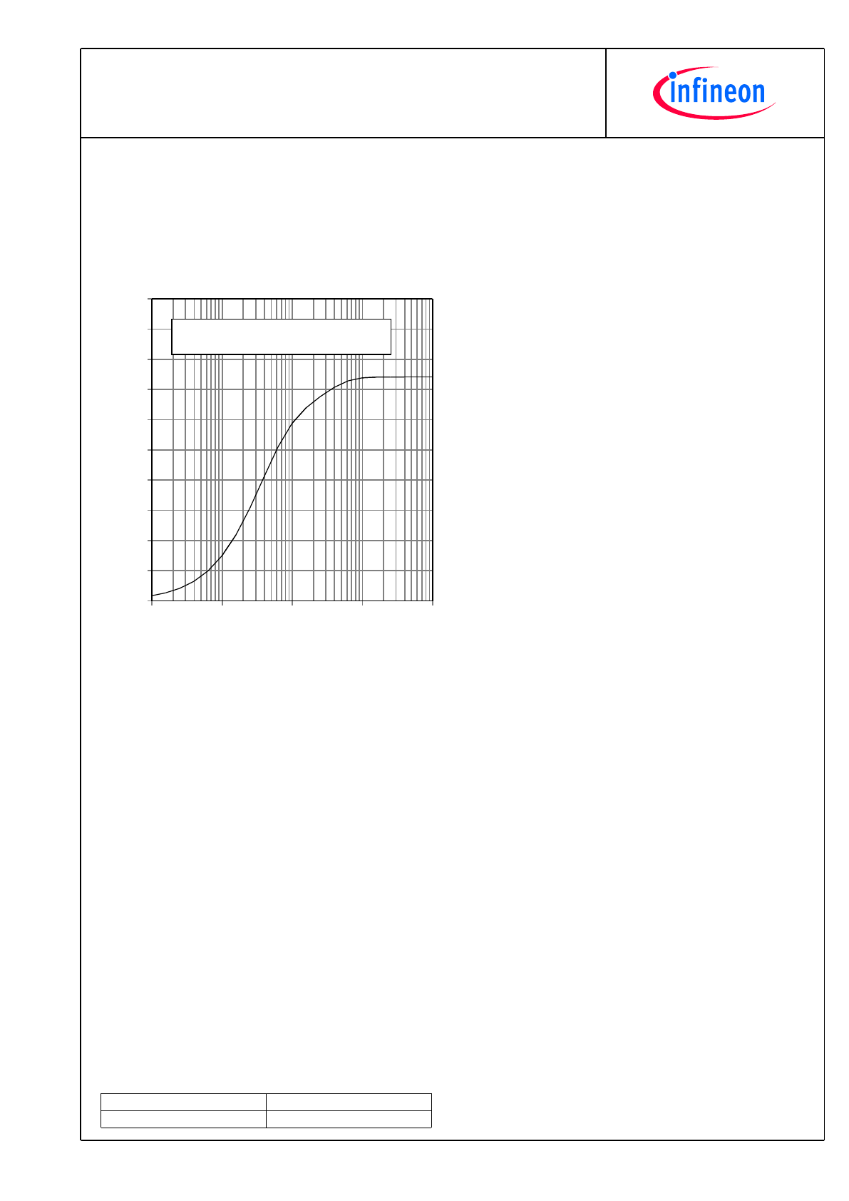
Analog temperature sensor output V
Theta NTC
Sensing NTC of IGBT module
T
NTC
[°C]
V
Theta NTC
[V]
20
30
40
50
60
70
80
90
100
0
1
2
3
4
5
6
7
8
9
10
11
12
5
TechnicalInformation
2LS20017E42W36702
ModSTACK™
preparedby:OW
approvedby:AR
dateofpublication:2013-10-08
revision:2.2
Preliminarydata
Z
th,ha
- thermal impedance heatsink to ambient per switch
nom. cooling conditions
t [s]
Z
th,ha
[K/W]
0.1
1
10
100
1000
0.000
0.005
0.010
0.015
0.020
0.025
0.030
0.035
0.040
0.045
0.050
i:
r
i
[K/W]:
τ
i
[s]:
1
0.000006
0.000001403
2
0.000006
0.00000451
3
0.0274
3.381
4
0.00964
22.97
6
TechnicalInformation
2LS20017E42W36702
ModSTACK™
preparedby:OW
approvedby:AR
dateofpublication:2013-10-08
revision:2.2
Preliminarydata
Mechanicaldrawing
1
H
2
3
4
5
6
7
8
9
10
11
12
1
2
3
4
5
6
8
7
G
F
E
D
C
B
A
H
G
F
E
D
C
B
A
9
10
11
12
C
op
yr
ig
ht
IN
FI
N
E
O
N
T
E
C
H
N
O
LO
G
IE
S
A
G
,A
ll
rig
ht
s
re
se
rv
ed
c
A
2
Do
ku
me
nts
ta
tu
ss
ie
he
SA
P-D
oku
me
nte
nve
rw
altu
ng
32
2x
M
,A
C-c
on
ne
ctin
po
in
t
to
rq
ue
:m
ax
32
Nm
10
95
.6
5
0.8
60
15
10
4.6
5
70
0.
5
57
0.
15
85
.5
66
.6
0.5
10
9
0.5
22
4
0.5
37
4
0.5
0
20
0
+0
.5
-1
.5
20
4.
65
1
117
.3
+1
-2
29
.5
0.5
75
.2
0.5
80
.5
0.1
5
10
0
0.1
5
32
4.5
0.1
5
34
4
0.1
5
0
DC
-P
lu
s
62
.5
DC
-M
in
us
66
.5
20
4.6
5
1
13
.1
5
37
.1
5
0.8
73
.1
5
90
0.8
39
9
0.8
0
19
.5
0.8
21
0.1
5
0.8
24
4.1
5
0.8
27
8.1
5
0.8
31
2.1
5
0.8
34
6.1
5
0.8
38
0.1
5
0.8
0
5.5
12
.5
P
ar
t-
N
o.
ge
ne
ra
lT
ol
er
an
ce
S
ur
fa
ce
S
ca
le
1:
2
A
ss
em
bl
y-
N
o.
D
IN
IS
O
27
68
-v
-
M
at
er
ia
l
M
at
er
ia
l-N
o.
D
at
e
N
am
e
D
es
ci
pt
io
n
A
ge
nt
6.
03
.1
2
P
ap
en
fo
rt
O
ut
lin
e
C
he
ck
ed
6.
03
.1
2
ge
z.
V
ol
ke
N
or
m
M
od
S
TA
C
K
C
G
ra
ph
-N
o.
V
er
si
on
S
he
et
36
70
2
M
b
0
Ve
rs
.
R
ev
is
io
n
D
at
e
N
am
e
O
rig
in
C
on
st
ru
ct
ed
fo
r
co
nn
ec
tin
g
po
in
ts
A
C
an
d
D
C
ar
e
tin
pl
at
ed
re
co
m
m
en
de
tt
or
qu
e:
D
C
+
an
d
D
C
-
M
8
:2
0N
m
+-
10
%
A
C
M
10
:3
2N
m
+-
10
%
M
6-
10
de
pt
h
4.
5-
5d
ep
th
3:
10
X
1:
ID
C
co
nn
ec
to
r
14
po
le
3x
M
8
D
C
-M
in
us
3x
M
8
D
C
-P
lu
s
G
1/
2"
w
at
er
ou
tle
t
M
10
,e
ar
th
gr
ou
nd
G
1/
2"
2x
M
4-
8d
ep
th
7
TechnicalInformation
2LS20017E42W36702
ModSTACK™
preparedby:OW
approvedby:AR
dateofpublication:2013-10-08
revision:2.2
Preliminarydata
Circuitdiagram
Top
Bottom
E
ic
eD
R
IV
E
R
T
M
AC
DC-
DC+
Signal
conditioning
&
Gate signals
Sensor
signals
Failure
management
Power
supply
DR240
Low voltage domain
1
X1 (IDC Connector)
14 pole male
X1:2
PWM BOT
X1:4
PWM TOP
X1:3
Fault
X1:5
OT Error
X1:8
P15 (50mA)
X1:9
P15 (50mA)
X1:6
P24
X1:7
P24
X1:10
GND
X1:11
GND
X1:14
V
I ana
X1:12
V
Theta NTC
X1:13
GND
analog
X1:1
TE, Shield
High voltage domain
T
NTC
Error Table
Error outputs (open collector)
X1:3
X1:5
Error driver core
Over temp. output stage
Over temperature PCB
Over voltage DC Link
Under voltage power supply
X = high level with external pull up resistor
Over current
x
x
x
x
x
x
M
od
S
T
A
C
K
T
M
DC+
DC-
8
TechnicalInformation
2LS20017E42W36702
ModSTACK™
preparedby:OW
approvedby:AR
dateofpublication:2013-10-08
revision:2.2
Preliminarydata
Terms&Conditionsofusage
Thedatacontainedinthisproductdatasheetisexclusivelyintendedfortechnicallytrainedstaff.Youandyourtechnical
departmentswillhavetoevaluatethesuitabilityoftheproductfortheintendedapplicationandthecompletenessoftheproduct
datawithrespecttosuchapplication.
Thisproductdatasheetisdescribingthecharacteristicsofthisproductforwhichawarrantyisgranted.Anysuchwarrantyis
grantedexclusivelypursuantthetermsandconditionsofthesupplyagreement.Therewillbenoguaranteeofanykindforthe
productanditscharacteristics.
Shouldyourequireproductinformationinexcessofthedatagiveninthisproductdatasheetorwhichconcernsthespecific
applicationofourproduct,pleasecontactthesalesoffice,whichisresponsibleforyou(seewww.infineon.com,sales&contact).
Forthosethatarespecificallyinterestedwemayprovideapplicationnotes.
Duetotechnicalrequirementsourproductmaycontaindangeroussubstances.Forinformationonthetypesinquestionplease
contactthesalesoffice,whichisresponsibleforyou.
ShouldyouintendtousetheProductinaviationapplications,inhealthorliveendangeringorlifesupportapplications,please
notify.Pleasenote,thatforanysuchapplicationsweurgentlyrecommend
-toperformjointRiskandQualityAssessments;
-theconclusionofQualityAgreements;
-toestablishjointmeasuresofanongoingproductsurvey,
andthatwemaymakedeliverydependedontherealization
ofanysuchmeasures.
Ifandtotheextentnecessary,pleaseforwardequivalentnoticestoyourcustomers.
Changesofthisproductdatasheetarereserved.
SafetyInstructions
Priortoinstallationandoperation,allsafetynoticesandwarningsandallwarningsignsattachedtotheequipmenthavetobe
carefullyread.Makesurethatallwarningsignsremaininalegibleconditionandthatmissingordamagedsignsarereplaced.To
installationandoperation,allsafetynoticesandwarningsandallwarningsignsattachedtotheequipmenthavetobecarefully
read.Makesurethatallwarningsignsremaininalegibleconditionandthatmissingordamagedsignsarereplaced.