

BTS5016SDA
Smart High-Side Power Switch
PROFET™
One Channel
Datasheet, Rev. 1.1, Nov. 2008
Automotive Power

Datasheet
2
Rev. 1.1, 2008-11-04
Smart High-Side Power Switch
BTS5016SDA
Table of Contents
1
Overview . . . . . . . . . . . . . . . . . . . . . . . . . . . . . . . . . . . . . . . . . . . . . . . . . . . . . . . . . . . . . . . . . . . . . . . 3
2
Block Diagram and Terms . . . . . . . . . . . . . . . . . . . . . . . . . . . . . . . . . . . . . . . . . . . . . . . . . . . . . . . . . 5
2.1
Block Diagram . . . . . . . . . . . . . . . . . . . . . . . . . . . . . . . . . . . . . . . . . . . . . . . . . . . . . . . . . . . . . . . . . . . 5
2.2
Terms . . . . . . . . . . . . . . . . . . . . . . . . . . . . . . . . . . . . . . . . . . . . . . . . . . . . . . . . . . . . . . . . . . . . . . . . . . 5
3
Pin Configuration . . . . . . . . . . . . . . . . . . . . . . . . . . . . . . . . . . . . . . . . . . . . . . . . . . . . . . . . . . . . . . . . 6
3.1
Pin Assignment BTS5016SDA . . . . . . . . . . . . . . . . . . . . . . . . . . . . . . . . . . . . . . . . . . . . . . . . . . . . . . . 6
3.2
Pin Definitions and Functions . . . . . . . . . . . . . . . . . . . . . . . . . . . . . . . . . . . . . . . . . . . . . . . . . . . . . . . . 6
4
General Product Characteristics . . . . . . . . . . . . . . . . . . . . . . . . . . . . . . . . . . . . . . . . . . . . . . . . . . . . 7
4.1
Absolute Maximum Ratings . . . . . . . . . . . . . . . . . . . . . . . . . . . . . . . . . . . . . . . . . . . . . . . . . . . . . . . . . 7
4.2
Thermal Resistance . . . . . . . . . . . . . . . . . . . . . . . . . . . . . . . . . . . . . . . . . . . . . . . . . . . . . . . . . . . . . . . 8
5
Power Stages . . . . . . . . . . . . . . . . . . . . . . . . . . . . . . . . . . . . . . . . . . . . . . . . . . . . . . . . . . . . . . . . . . . 9
5.1
Input Circuit . . . . . . . . . . . . . . . . . . . . . . . . . . . . . . . . . . . . . . . . . . . . . . . . . . . . . . . . . . . . . . . . . . . . . . 9
5.2
Output On-State Resistance . . . . . . . . . . . . . . . . . . . . . . . . . . . . . . . . . . . . . . . . . . . . . . . . . . . . . . . . 10
5.3
Output Inductive Clamp . . . . . . . . . . . . . . . . . . . . . . . . . . . . . . . . . . . . . . . . . . . . . . . . . . . . . . . . . . . 11
5.3.1
Maximum Load Inductance . . . . . . . . . . . . . . . . . . . . . . . . . . . . . . . . . . . . . . . . . . . . . . . . . . . . . . . 11
5.4
Electrical Characteristics . . . . . . . . . . . . . . . . . . . . . . . . . . . . . . . . . . . . . . . . . . . . . . . . . . . . . . . . . . 13
6
Protection Functions . . . . . . . . . . . . . . . . . . . . . . . . . . . . . . . . . . . . . . . . . . . . . . . . . . . . . . . . . . . . 15
6.1
Overload Protection . . . . . . . . . . . . . . . . . . . . . . . . . . . . . . . . . . . . . . . . . . . . . . . . . . . . . . . . . . . . . . 15
6.2
Short circuit impedance . . . . . . . . . . . . . . . . . . . . . . . . . . . . . . . . . . . . . . . . . . . . . . . . . . . . . . . . . . . 16
6.3
Reverse Polarity Protection - Reversave™ . . . . . . . . . . . . . . . . . . . . . . . . . . . . . . . . . . . . . . . . . . . . 17
6.4
Overvoltage Protection . . . . . . . . . . . . . . . . . . . . . . . . . . . . . . . . . . . . . . . . . . . . . . . . . . . . . . . . . . . . 18
6.5
Loss of Ground Protection . . . . . . . . . . . . . . . . . . . . . . . . . . . . . . . . . . . . . . . . . . . . . . . . . . . . . . . . . 18
6.6
Loss of Vbb Protection . . . . . . . . . . . . . . . . . . . . . . . . . . . . . . . . . . . . . . . . . . . . . . . . . . . . . . . . . . . . 18
6.7
Electrical Characteristics . . . . . . . . . . . . . . . . . . . . . . . . . . . . . . . . . . . . . . . . . . . . . . . . . . . . . . . . . . 19
7
Diagnosis . . . . . . . . . . . . . . . . . . . . . . . . . . . . . . . . . . . . . . . . . . . . . . . . . . . . . . . . . . . . . . . . . . . . . . 21
7.1
Electrical Characteristics . . . . . . . . . . . . . . . . . . . . . . . . . . . . . . . . . . . . . . . . . . . . . . . . . . . . . . . . . . 23
8
Package Outlines . . . . . . . . . . . . . . . . . . . . . . . . . . . . . . . . . . . . . . . . . . . . . . . . . . . . . . . . . . . . . . . 24
9
Revision History . . . . . . . . . . . . . . . . . . . . . . . . . . . . . . . . . . . . . . . . . . . . . . . . . . . . . . . . . . . . . . . . 25
Table of Contents
PG-TO252-5-11
Type
Package
Marking
BTS5016SDA
PG-TO252-5-11
5016SDA
Datasheet
3
Rev. 1.1, 2008-11-04
Smart High-Side Power Switch
PROFET™
One Channel
BTS5016SDA
1
Overview
Features
•
Part of scalable product family
•
Load current sense
•
Reversave™
•
Very low standby current
•
Current controlled input pin
•
Improved electromagnetic compatibility (EMC)
•
Fast demagnetization of inductive loads
•
Stable behavior at under-voltage
•
Green Product (RoHS compliant)
•
AEC Qualified
The BTS5016SDA is a one channel high-side power switch in PG-TO252-5-11 package providing embedded
protective functions.
The power transistor is built by a N-channel vertical power MOSFET with charge pump. The design is based on
Smart SIPMOS chip on chip technology.
The BTS5016SDA has a current controlled input and offers a diagnostic feedback with load current sense and a
defined fault signal in case of overload operation, overtemperature shutdown and/or short circuit shutdown.
Operating voltage
V
bb(on)
5.5 .. 20 V
Minimum overvoltage protection
V
ON(CL)
39 V
Maximum on-state resistance at
T
j
= 150 °C
R
DS(ON)
32 m
Ω
Nominal load current
I
L(nom)
5.5 A
Minimum current limitation
I
L4(SC)
45 A
Maximum stand-by current for whole device with load at
T
j
= 25 °C
I
bb(OFF)
6 µA

Smart High-Side Power Switch
BTS5016SDA
Overview
Datasheet
4
Rev. 1.1, 2008-11-04
Protective Functions
•
Reversave™, channel switches on in case of reverse polarity
•
Reverse battery protection without external components
•
Short circuit protection with latch
•
Overload protection
•
Multi-step current limitation
•
Thermal shutdown with restart
•
Overvoltage protection (including load dump)
•
Loss of ground protection
•
Loss of V
bb
protection (with external diode for charged inductive loads)
•
Electrostatic discharge protection (ESD)
Diagnostic Functions
•
Proportional load current sense (with defined fault signal in case of overload operation, overtemperature
shutdown and/or short circuit shutdown)
•
Open load detection in ON-state by load current sense
Applications
•
µC compatible high-side power switch with diagnostic feedback for 12 V grounded loads
•
All types of resistive, inductive and capacitive loads
•
Most suitable for loads with high inrush currents, so as lamps
•
Replaces electromechanical relays, fuses and discrete circuits
Datasheet
5
Rev. 1.1, 2008-11-04
Smart High-Side Power Switch
BTS5016SDA
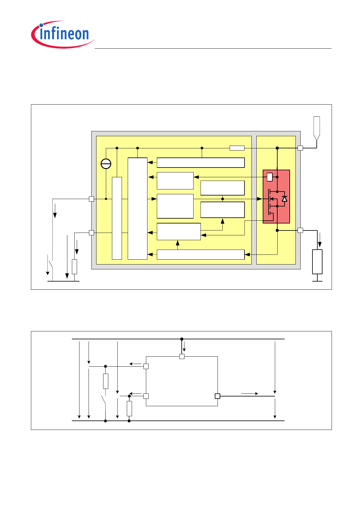
Block Diagram and Terms
2
Block Diagram and Terms
2.1
Block Diagram
Figure 1
Block Diagram
2.2
Terms
Following figure shows all terms used in this data sheet.
Figure 2
Terms
logic IC
base chip
V
bb
IS
OUT
IN
LOAD
ES
D
R
IS
V
IS
V
IN
I
IN
I
L
Overview .emf
T
driver
logic
gate control
&
charge pump
load current
sense
over
temperature
clamp for
inductive load
current
limitation
forward voltage drop detection
voltage sensor
I
IS
R
bb
Terms.emf
V
IN
OUT
V
IS
I
IS
V
bb
I
L
V
OUT
I
bb
IN
VBB
IS
I
IN
V
bIN
V
bIS
V
ON
R
IN
R
IS
BTS5016SDA
Smart High-Side Power Switch
BTS5016SDA
Pin Configuration
Datasheet
6
Rev. 1.1, 2008-11-04
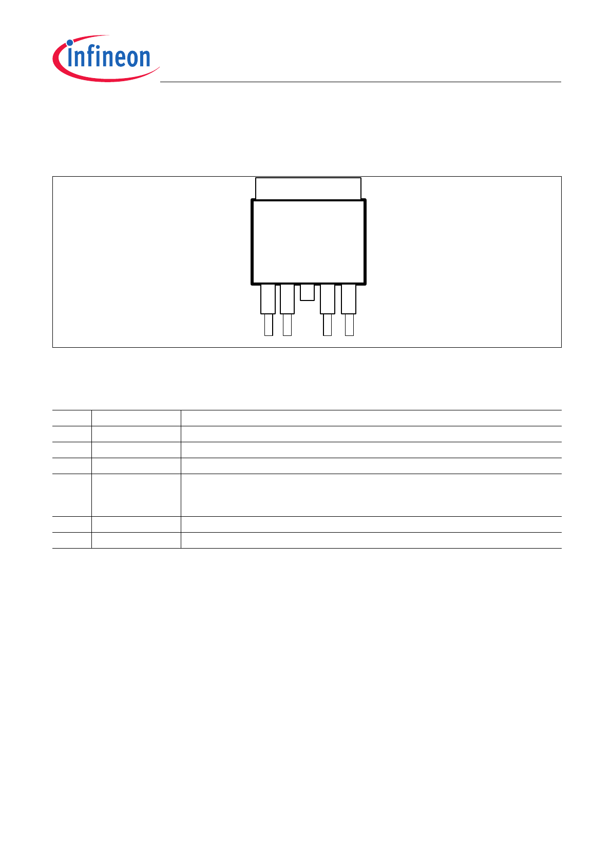
3
Pin Configuration
3.1
Pin Assignment BTS5016SDA
Figure 3
Pin Configuration
3.2
Pin Definitions and Functions
Pin
Symbol
Function
1
OUT
Output; output to the load; pin 1 and 5 must be externally shorted.
1)
1) Not shorting all outputs will considerably increase the on-state resistance, reduce the peak current capability, the clamping
capability and decrease the current sense accuracy.
2
IN
Input; activates the power switch if shorted to ground.
3
V
bb
Supply Voltage; positive power supply voltage; tab and pin 3 are internally shorted.
4
IS
Sense Output; Diagnostic feedback; provides at normal operation a sense current
proportional to the load current; in case of overload, overtemperature and/or short
circuit a defined current is provided (see
Table 1 “Truth Table” on Page 21
).
5
OUT
Output; output to the load; pin 1 and 5 must be externally shorted.
1)
TAB
V
bb
Supply Voltage; positive power supply voltage; tab and pin 3 are internally shorted.
V
bb
TAB
1
2
3
4
5
OU
T
OU
T
IN
IS
V
bb
TO252-5.emf

Datasheet
7
Rev. 1.1, 2008-11-04
Smart High-Side Power Switch
BTS5016SDA
General Product Characteristics
4
General Product Characteristics
4.1
Absolute Maximum Ratings
Note: Stresses above the ones listed here may cause permanent damage to the device. Exposure to absolute
maximum rating conditions for extended periods may affect device reliability.
Absolute Maximum Ratings
1)
T
j
= 25 °C (unless otherwise specified)
1) Not subject to production test, specified by design.
Pos.
Parameter
Symbol
Limit Values
Unit
Conditions
Min.
Max.
Supply Voltages
4.1.1
Supply voltage
V
bb
-16
38
V
–
4.1.2
Supply voltage for short circuit protection
(single pulse)
2)
2) Short circuit is defined as a combination of remaining resistances and inductances. See
Figure 13
.
V
bb(SC)
0
20
V
–
4.1.3
Supply Voltage for Load Dump
protection
3)
3) Load Dump is specified in ISO 7637, R
I
is the internal resistance of the Load Dump pulse generator.
V
bb(LD)
–
45
V
R
I
= 2
Ω,
R
L
= 1.5
Ω,
Logic Pins
4.1.4
Voltage at input pin
V
bIN
-16
63
V
–
4.1.5
Current through input pin
I
IN
-140
15
mA
–
4.1.6
Voltage at current sense pin
V
bIS
-16
63
V
–
4.1.7
Current through sense pin
I
IS
-140
15
mA
–
4.1.8
Input voltage slew rate
4)
4) Slew rate limitation can be achieved by means of using a series resistor for the small signal driver or in series in the input
path. A series resistor
R
IN
in the input path is also required for reverse operation at
V
bb
≤-16V. See also
Figure 14
.
dV
bIN
/dt
-20
20
V/µs
–
Power Stages
4.1.9
Load current
5)
5) Current limitation is a protection feature. Operation in current limitation is considered as “outside” normal operating range.
Protection features are not designed for continuous repetitive operation.
I
L
-
I
Lx(SC)
A
–
4.1.10
Maximum energy dissipation per
channel (single pulse)
E
AS
-
0.12
J
V
bb
= 12 V,
I
L(0)
= 20 A,
T
j(0)
= 150 °C
Temperatures
4.1.11
Junction temperature
T
j
-40
150
°C
–
4.1.12
Storage temperature
T
stg
-55
150
°C
–
ESD Susceptibility
4.1.13
ESD susceptibility HBM
Pin 2 (IN)
Pin 4 (IS)
Pin1/5 (OUT)
V
ESD
-2
-2
-4
2
2
4
kV
according to
EIA/JESD 22-A
114B

Smart High-Side Power Switch
BTS5016SDA
General Product Characteristics
Datasheet
8
Rev. 1.1, 2008-11-04
Note: Integrated protection functions are designed to prevent IC destruction under fault conditions described in the
data sheet. Fault conditions are considered as “outside” normal operating range. Protection functions are
not designed for continuous repetitive operation.
4.2
Thermal Resistance
Pos.
Parameter
Symbol
Limit Values
Unit
Conditions
Min.
Typ.
Max.
4.2.1
Junction to Case
1)
1) Not subject to production test, specified by design.
R
thjc
–
–
1.3
K/W
–
4.2.2
Junction to Ambient
1)
free air
device on PCB
2)
device on PCB
3)
2) Device mounted on PCB (50 mm x 50 mm x 1.5mm epoxy, FR4) with 6 cm
2
copper heatsinking area (one layer, 70 µm
thick) for
V
bb
connection. PCB is vertical without blown air.
3) Specified
R
thJA
value is according to Jedec JESD51-2,-5,-7 at natural convection on FR4 2s2p board; The Product
(Chip+Package) was simulated on a 76.2 x 114.3 x 1.5 mm board with 2 inner copper layers (2 x 70µm Cu, 2 x 35µm Cu).
Where applicable a thermal via array under the exposed pad contacted the first inner copper layer.
R
thja
-
-
-
80
45
22
-
-
-
K/W
–
Datasheet
9
Rev. 1.1, 2008-11-04
Smart High-Side Power Switch
BTS5016SDA
Power Stages
5
Power Stages
The power stage is built by a N-channel vertical power MOSFET (DMOS) with charge pump.
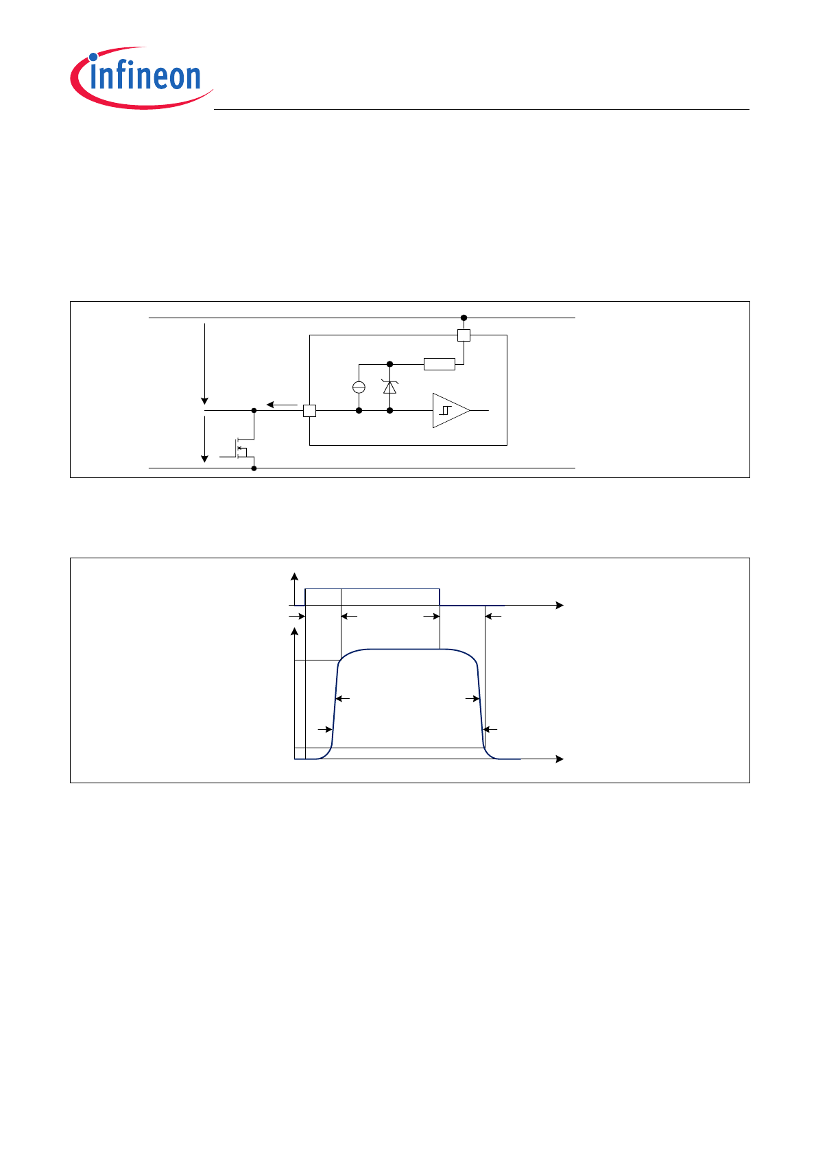
5.1
Input Circuit
Figure 4
shows the input circuit of the BTS5016SDA. The current source to V
bb
ensures that the device switches
off in case of open input pin. The zener diode protects the input circuit against ESD pulses.
Figure 4
Input Circuit
A high signal at the required external small signal transistor pulls the input pin to ground. A logic supply current
I
IN
is flowing and the power DMOS switches on with a dedicated slope, which is optimized in terms of EMC emission.
Figure 5
Switching a Load (resistive)
IN
R
bb
I
V
bb
Input.emf
V
Z,IN
V
IN
I
IN
V
bIN
V
OUT
t
SwitchOn.emf
t
I
IN
10%
25%
50%
90%
t
ON
t
OFF
(dV/dt)
ON
(dV/dt)
OFF
Smart High-Side Power Switch
BTS5016SDA
Power Stages
Datasheet
10
Rev. 1.1, 2008-11-04
5.2
Output On-State Resistance
The on-state resistance
R
DS(ON)
depends on the supply voltage as well as the junction temperature
T
j
.
Figure 6
shows these dependencies for the typical on-state resistance. The voltage drop in reverse polarity mode is
described in
Section 6.3
.
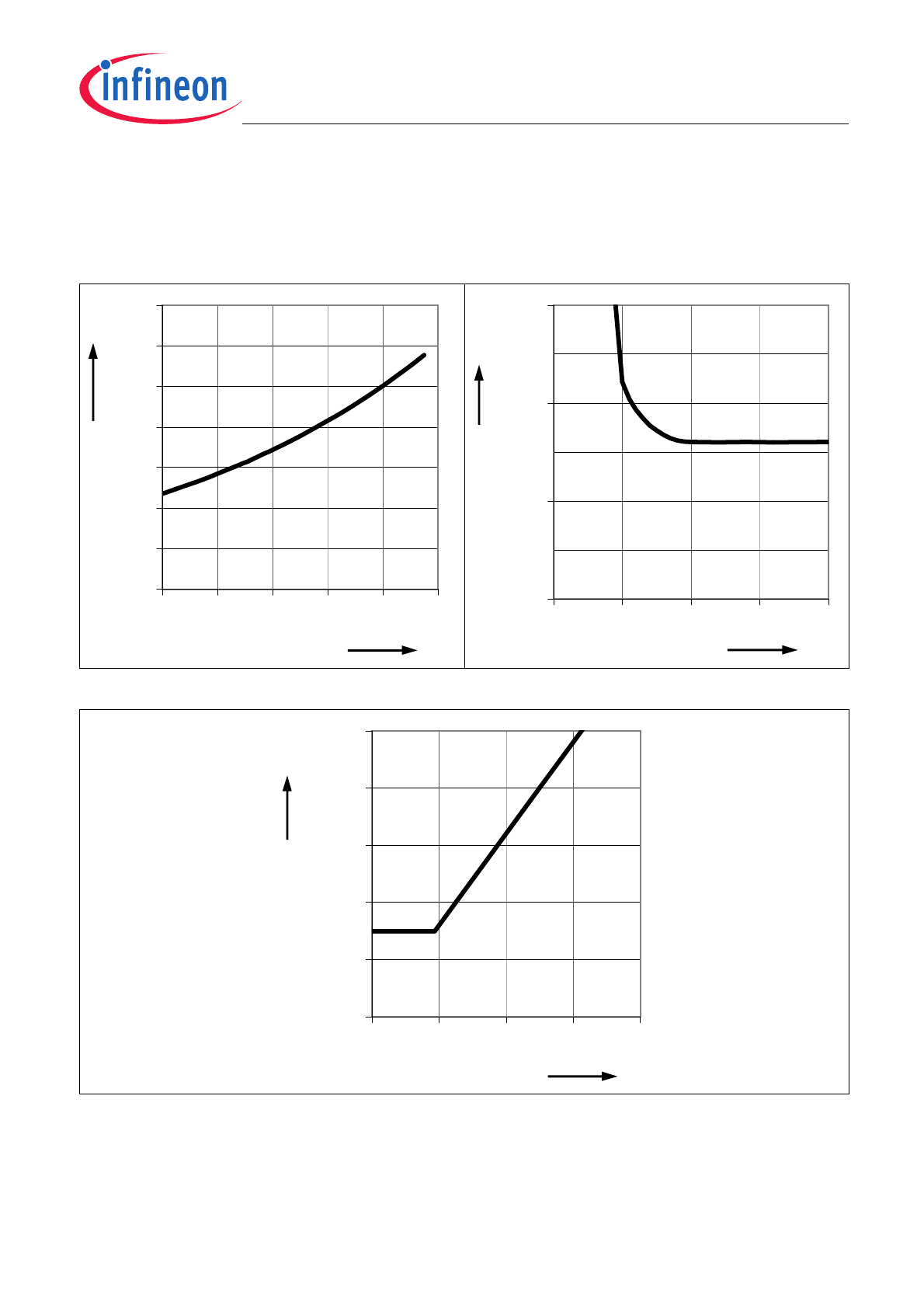
Figure 6
Typical On-State Resistance
Figure 7
Typical Output Voltage Drop Limitation
5
'621
9
EE
9
W\S
Pȍ
,
/
$
7
M
Pȍ
&
W\S
5
'621
,
/
$
V
bb
= 12 V
T
j
= 25°C
9
21
,
/
W\S
9
21
a,
/
$
9
9
21
≥ 9
211/